


Motorola MAC6075A, MAC6073B, MAC6071B, MAC6071A, MAC6075B Datasheet
...
MOTOROLA
SEMICONDUCTOR TECHNICAL DATA
Order this document by MAC6071/D
Advance Information
Sensitive Gate Triacs
Silicon Bidirectional Thyristors
. . . designed primarily for full-wave ac control applications, such as light dimmers, motor controls, heating controls and power supplies; or wherever full-wave silicon gate controlled solid-state devices are needed. Triac type thyristors switch from a blocking to a conducting state for either polarity of applied anode voltage with positive or negative gate triggering.
•Sensitive Gate Triggering (A and B versions) Uniquely Compatible for Direct Coupling to TTL, HTL, CMOS and Operational Amplifier Integrated Circuit Logic Functions
•Gate Triggering 4 Mode Ð MAC6071A,B, MAC6073A,B, MAC6075A,B
•Blocking Voltages to 600 Volts
•All Diffused and Glass Passivated Junctions for Greater Parameter Uniformity and Stability
•Small, Rugged, Thermopad Construction for Low Thermal Resistance, High Heat Dissipation and Durability
MAC6071A,B* MAC6073A,B* MAC6075A,B*
*Motorola preferred devices
TRIACs
4 AMPERES RMS
200 thru 600 VOLTS
MT1
MT2 |
G |
|
|
|
MT2 |
|
|
|
|
G |
CASE 77-08 |
|
|
|
|
|
(TO-225AA) |
||
|
|
|
|
MT2 MT1 |
||
|
|
|
|
|
STYLE 5 |
|
MAXIMUM RATINGS (TJ = 25°C unless otherwise noted) |
|
|
|
|
|
|
|
|
|
|
|
||
|
|
|
|
|
|
|
|
Rating |
Symbol |
Value |
|
Unit |
|
|
|
|
|
|
|
|
Peak Repetitive Off-State Voltage(1) |
|
VDRM |
|
|
Volts |
|
(Gate Open, TJ = 25 to 110°C) |
MAC6071A,B |
|
|
200 |
|
|
|
MAC6073A,B |
|
|
400 |
|
|
|
MAC6075A,B |
|
|
600 |
|
|
|
|
|
|
|
|
|
On-State Current RMS (TC = 85°C) |
|
IT(RMS) |
4 |
|
Amps |
|
Peak Surge Current (One Full cycle, 60 Hz, TJ = ±40 to +110°C) |
ITSM |
30 |
|
Amps |
||
Circuit Fusing Considerations (t = 8.3 ms) |
I2t |
3.7 |
|
A2s |
||
Peak Gate Power |
|
PGM |
10 |
|
Watts |
|
Average Gate Power |
|
PG(AV) |
0.5 |
|
Watt |
|
Peak Gate Voltage |
|
VGM |
5 |
|
Volts |
|
Operating Junction Temperature Range |
TJ |
±40 to +110 |
|
°C |
||
Storage Temperature Range |
|
Tstg |
±40 to +150 |
|
°C |
|
Mounting Torque (6-32 Screw)(2) |
|
Ð |
|
8 |
|
in. lb. |
1.VDRM for all types can be applied on a continuous basis. Blocking voltages shall not be tested with a constant current source such that the voltage ratings of the devices are exceeded.
2.Torque rating applies with use of compression washer (B52200F006). Mounting torque in excess of 6 in. lb. does not appreciably lower
case-to-sink thermal resistance. Main terminal 2 and heatsink contact pad are common.
For soldering purposes (either terminal connection or device mounting), soldering temperatures shall not exceed +200°C, for 10 seconds. Consult factory for lead bending options.
This document contains information on a new product. Specifications and information herein are subject to change without notice.
Preferred devices are Motorola recommended choices for future use and best overall value.
Motorola, Inc. 1996

MAC6071A,B |
MAC6073A,B MAC6075A,B |
|
|
|
|
|
|
|
|
|
|
|
THERMAL CHARACTERISTICS |
|
|
|
|
|
|
|
|
|
|
|
|
|
|
|
|
|
|
|
|
|
|
|
|
|
|
Characteristic |
|
|
Symbol |
|
Max |
|
|
Unit |
|||
|
|
|
|
|
|
|
|
|
|
|
||
Thermal Resistance, Junction to Case |
|
|
RθJC |
3.5 |
|
|
°C/W |
|||||
Thermal Resistance, Junction to Ambient |
|
|
RθJA |
75 |
|
|
°C/W |
|||||
ELECTRICAL CHARACTERISTICS (TC = 25°C unless otherwise noted) |
|
|
|
|
|
|
|
|
|
|
||
|
|
|
|
|
|
|
|
|
|
|||
|
Characteristic |
Symbol |
|
Min |
|
Typ |
Max |
|
Unit |
|||
|
|
|
|
|
|
|
|
|
|
|
||
Peak Blocking Current |
(TJ = 25°C) |
IDRM |
|
Ð |
|
Ð |
10 |
|
μA |
|||
(VD = Rated VDRM, gate open) |
|
|
|
|
|
|||||||
|
|
(TJ = 110°C) |
|
|
|
Ð |
|
Ð |
2.0 |
|
mA |
|
On-State Voltage (Either Direction) |
|
VTM |
|
Ð |
|
1.3 |
2.0 |
|
Volts |
|||
(ITM = 6 A Peak) |
|
|
|
|
|
|
|
|
|
|
|
|
Peak Gate Trigger Voltage (Continuous dc) |
VGT |
|
|
|
|
|
|
|
Volts |
|||
(TJ = ±40°C) (Main Terminal Voltage = 12 Vdc, RL = 100 Ohms) |
|
|
|
|
|
|
|
|
|
|
||
MT2(+), G(+); MT2(±), G(±) |
|
|
|
|
0.5 |
|
0.8 |
1.9 |
|
|
||
MT2(+), G(±); MT2(±), G(+) |
|
|
|
|
0.5 |
|
0.8 |
1.9 |
|
|
||
(TJ = 110°C) |
|
|
|
|
|
|
|
|
|
|
|
|
MT2(+), G(+); MT2(±), G(±) |
|
|
|
|
0.2 |
|
0.4 |
0.9 |
|
|
||
MT2(+), G(±); MT2(±), G(+) |
|
|
|
|
0.2 |
|
0.4 |
0.9 |
|
|
||
(TJ = 25°C) |
|
|
|
|
|
|
|
|
|
|
|
|
MT2(+), G(+); MT2(±), G(±) |
|
|
|
|
0.4 |
|
0.7 |
1.4 |
|
|
||
MT2(+), G(±); MT2(±), G(+) |
|
|
|
|
0.4 |
|
0.7 |
1.4 |
|
|
||
|
|
|
|
|
|
|
|
|
|
|
||
Holding Current (Either Direction) |
|
IH |
|
|
|
|
|
|
|
mA |
||
(TJ = ±40°C) (Main Terminal Voltage = 12 Vdc, Gate Open) |
|
|
|
|
|
|
|
|
|
|
||
(Initiating Current = 150 mA) |
|
|
|
|
0.4 |
|
2.0 |
10 |
|
|
||
(TJ = 25°C) |
|
|
|
|
|
0.2 |
|
1.0 |
5.0 |
|
|
|
Latching Current |
(VD = 6 V) |
TJ = 25°C |
IL |
|
Ð |
|
2.0 |
10 |
|
mA |
||
MT2(+), G(+) |
(IG = 8 mA) |
|
|
|
|
|
|
|||||
MT2(+), G(±) |
(IG = 8 mA) |
|
|
|
|
Ð |
|
5.0 |
20 |
|
|
|
MT2(±), G(±) |
(IG = 8 mA) |
|
|
|
|
Ð |
|
1.0 |
10 |
|
|
|
MT2(±), G(+) |
(IG = 15 mA) |
|
|
|
|
Ð |
|
2.0 |
10 |
|
|
|
Gate Trigger Current (Continuous dc) |
|
IGT |
|
|
|
|
|
|
|
mA |
||
(VD = 12 Vdc, RL = 100 Ohms) |
|
|
|
|
|
|
|
|
|
|
|
|
MAC6071A, MAC6073A, MAC6075A |
|
|
|
|
|
|
|
|
|
|
||
MT2(+), G(+) |
|
TJ = 25°C |
|
|
|
0.4 |
|
2.0 |
5.0 |
|
|
|
MT2(+), G(±) |
|
|
|
|
|
0.4 |
|
3.0 |
5.0 |
|
|
|
MT2(±), G(±) |
|
|
|
|
|
0.4 |
|
3.0 |
5.0 |
|
|
|
MT2(±), G(+) |
|
|
|
|
|
0.8 |
|
4.5 |
10 |
|
|
|
MT2(+), G(+) |
|
TJ = ±40°C |
|
|
|
0.8 |
|
3.5 |
10 |
|
|
|
MT2(+), G(±) |
|
|
|
|
|
0.8 |
|
4.5 |
10 |
|
|
|
MT2(±), G(±) |
|
|
|
|
|
0.8 |
|
5.0 |
10 |
|
|
|
MT2(±), G(+) |
|
|
|
|
|
1.6 |
|
10 |
20 |
|
|
|
|
|
|
|
|
|
|
|
|
|
|
|
|
2 |
Motorola Thyristor Device Data |
|
|
MAC6071A,B |
MAC6073A,B |
MAC6075A,B |
|||||
ELECTRICAL CHARACTERISTICS (TC = 25°C unless otherwise noted) |
|
|
|
|
|
|
|
|
|
Characteristic |
|
Symbol |
Min |
Typ |
|
Max |
Unit |
|
|
|
|
|
|
|
|
|
|
|
|
Gate Trigger Current (Continuous dc) |
|
|
IGT |
|
|
|
|
mA |
|
(VD = 12 Vdc, RL = 100 Ohms) |
|
|
|
|
|
|
|
|
|
MAC6071B, MAC6073B, MAC6075B |
|
|
|
|
|
|
|
|
|
MT2(+), G(+) |
TJ = 25°C |
|
|
0.4 |
1.5 |
|
3.0 |
|
|
MT2(+), G(±) |
|
|
|
0.4 |
2.5 |
|
3.0 |
|
|
MT2(±), G(±) |
|
|
|
0.4 |
2.5 |
|
3.0 |
|
|
MT2(±), G(+) |
|
|
|
0.8 |
3.5 |
|
5.0 |
|
|
MT2(+), G(+) |
TJ = ±40°C |
|
|
0.8 |
3.0 |
|
8.0 |
|
|
MT2(+), G(±) |
|
|
|
0.8 |
4.0 |
|
8.0 |
|
|
MT2(±), G(±) |
|
|
|
0.8 |
4.5 |
|
8.0 |
|
|
MT2(±), G(+) |
|
|
|
1.6 |
7.5 |
|
15 |
|
|
|
|
|
|
|
|
|
|
|
|
Turn-On Time (Either Direction) |
|
|
tgt |
Ð |
1.5 |
|
Ð |
μs |
|
(ITM = 14 Adc, IGT = 100 mAdc) |
|
|
|
|
|
|
|
|
|
DYNAMIC CHARACTERISTICS |
|
|
|
|
|
|
|
|
|
|
|
|
|
|
|
|
|||
Characteristic |
|
Symbol |
Min |
Typ |
|
Max |
Unit |
|
|
|
|
|
|
|
|
|
|
|
|
Critical Rate of Rise of Off±State Voltage |
|
(di/dt)c |
|
|
|
|
A/ms |
|
|
(VD = 200 V, ITM = 1.4 A, Commutating dv/dt = 0.5 Vm/sec, |
|
|
Ð |
2.2 |
|
Ð |
|
|
|
Gate Open, TJ = 110°C, f = 250 Hz, Snubber: CS = 0.1 mF, RS = 56 W, |
|
|
|
|
|
|
|
|
|
see Figure 16) |
|
|
|
|
|
|
|
|
|
|
|
|
|
|
|
|
|
|
|
Critical Rate of Rise of Off±State Voltage |
|
dv/dt |
Ð |
7.0 |
|
Ð |
V/ms |
|
|
(VD = Rate VDRM, Exponential Waveform, RGK = OPEN, TJ = 110°C) |
|
|
|
|
|
|
|
|
|
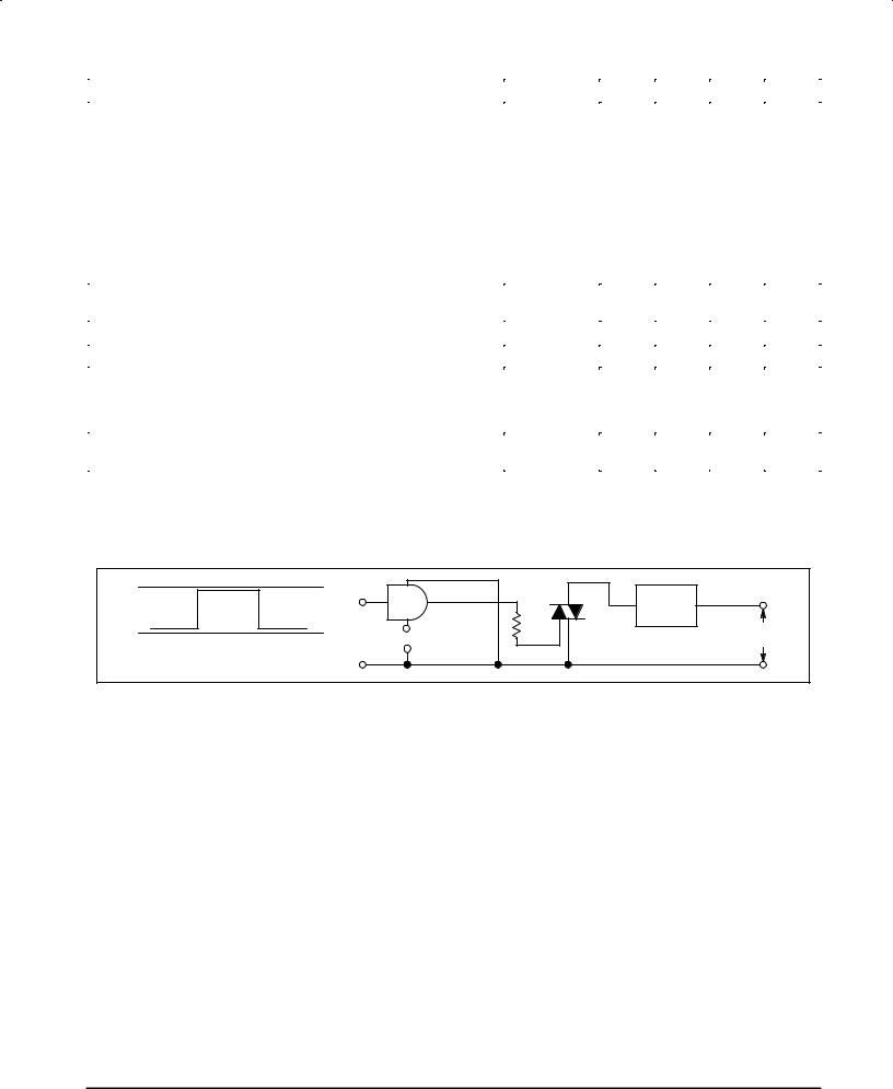
SAMPLE APPLICATION:
TTL-SENSITIVE GATE 4 AMPERE TRIAC
TRIGGERS IN MODES II AND III
0 V |
14 |
|
|
MC7400 |
|
|
|
|
|
LOAD |
|
|
4 |
|
|
|
510 |
2N6071A |
|
|
7 |
115 VAC |
|
±VEE |
Ω |
||
|
VEE = 5.0 V |
|
60 Hz |
|
+ |
|
|
QUADRANT DEFINITIONS
|
|
MT2(+) |
||
|
QUADRANT II |
|
QUADRANT I |
|
|
||||
|
MT2(+), G(±) |
|
MT2(+), G(+) |
|
G(±) |
|
|
|
G(+) |
|
|
|
||
QUADRANT III |
|
QUADRANT IV |
||
|
MT2(±), G(±) |
|
MT2(±), G(+) |
|
|
|
|
|
|
|
|
MT2(±) |
||
NOTES: For detail Digital Interfacing and Silicon Bilateral Switch (SBS) trigger application information, see the Motorola's Thyristor Data Book (DL137/D, Revision 6).
1.Interfacing Digital Circuits to Thyristor Controlled AC Loads, page 1.6±25.
2.Silicon Bilateral Switch (SBS) Applications, page 1.6±41.
Motorola Thyristor Device Data |
3 |
 Loading...