


|
|
|
|
|
|
|
|
|
|
|
Order this document by LM2574/D |
|||
|
|
|
|
|
|
|
|
|
|
|
LM2574 |
|||
|
|
|
|
|
|
|
|
|
|
|
||||
Advance |
Information |
|
|
|
|
|
|
|
|
|||||
Easy |
Switcher |
0.5 |
A |
|
|
|
|
|
||||||
|
|
|
|
|
||||||||||
Step-Down |
Voltage |
Regulator |
|
EASY SWITCHER |
||||||||||
The LM2574 series of regulators are monolithic integrated circuits ideally |
|
0.5 A STEP±DOWN |
||||||||||||
|
VOLTAGE REGULATOR |
|||||||||||||
suited for easy and convenient design of a step±down switching regulator |
|
|||||||||||||
(buck converter). All circuits of this series are capable of driving a 0.5 A load |
|
|
|
|
|
|||||||||
with excellent line and load regulation. These devices are available in fixed |
|
SEMICONDUCTOR |
||||||||||||
output voltages of 3.3 V, 5.0 V, 12 V, 15 V, and an adjustable output version. |
|
TECHNICAL DATA |
||||||||||||
These regulators were designed to minimize the number of external |
|
|
|
|
|
|||||||||
components to simplify the power supply design. Standard series of |
|
|
|
|
||||||||||
inductors optimized for use with the LM2574 are offered by several different |
|
|
|
|
|
|||||||||
inductor manufacturers. |
|
|
|
|
|
|
|
|
|
|
|
|
||
Since the LM2574 converter is a switch±mode power supply, its efficiency |
|
|
|
|
|
|||||||||
is significantly higher in comparison with popular three±terminal linear |
|
|
|
|
|
|||||||||
regulators, especially with higher input voltages. In most cases, the power |
|
|
|
|
|
|||||||||
dissipated by the LM2574 regulator is so low, that the copper traces on the |
|
|
|
|
|
|||||||||
printed circuit board are normally the only heatsink needed and no additional |
|
8 |
|
|
|
|||||||||
heatsinking is required. |
|
|
|
|
|
|
|
|
|
1 |
|
|
||
The LM2574 features include a guaranteed ±4% tolerance on output |
|
|
|
|
|
|||||||||
voltage within specified input voltages and output load conditions, and ±10% |
|
|
|
|
|
|||||||||
on the oscillator frequency (±2% over 0°C to +125°C). External shutdown is |
|
|
N SUFFIX |
|
||||||||||
included, featuring |
60 μA |
(typical) standby current. The output switch |
|
|
|
|||||||||
|
PLASTIC PACKAGE |
|||||||||||||
includes cycle±by±cycle current limiting, as well as thermal shutdown for full |
|
|||||||||||||
|
|
CASE 626 |
|
|||||||||||
protection under fault conditions. |
|
|
|
|
|
|
|
|
|
|
|
|||
Features |
|
|
|
|
|
|
|
|
|
|
|
|
|
|
|
|
|
|
|
|
|
|
|
|
|
|
|
|
|
• 3.3 V, 5.0 V, 12 V, 15 V, and Adjustable Output Versions |
|
PIN CONNECTIONS |
||||||||||||
• Adjustable Version Output Voltage Range, 1.23 to 37 V ±4% max over |
|
|||||||||||||
|
|
|
|
|
||||||||||
Line and Load Conditions |
|
|
|
|
|
|
|
|
|
|
|
|
||
• Guaranteed 0.5 A Output Current |
|
|
|
|
|
|
|
FB |
1 |
8 |
* |
|||
• Wide Input Voltage Range: 4.75 to 40 V |
|
|
|
|
|
|
|
Sig Gnd |
2 |
7 |
Output |
|||
|
|
|
|
|
|
|
ON/OFF |
3 |
6 |
* |
||||
• Requires Only 4 External Components |
|
|
|
|
|
|
|
|||||||
|
|
|
|
|
|
|
Pwr Gnd |
4 |
5 |
Vin |
||||
• 52 kHz Fixed Frequency Internal Oscillator |
|
|
|
|
|
(Top View) |
|
|
||||||
• TTL Shutdown Capability, Low Power Standby Mode |
|
|
|
|
|
|||||||||
• High Efficiency |
|
|
|
|
|
|
|
|
|
* No internal connection, but should be soldered to |
||||
• Uses Readily Available Standard Inductors |
|
|
|
|
||||||||||
|
|
|
|
* PC board for best heat transfer. |
|
|||||||||
• Thermal Shutdown and Current Limit Protection |
|
|
|
|
|
|
|
|
||||||
|
|
|
|
|
|
|
|
|||||||
Applications
•Simple and High±Efficiency Step±Down (Buck) Regulators
•Efficient Pre±regulator for Linear Regulators
•On±Card Switching Regulators
•Positive to Negative Converters (Buck±Boost)
•Negative Step±Up Converters
•Power Supply for Battery Chargers
This document contains information on a new product. Specifications and information herein are subject to change without notice.
DEVICE TYPE/NOMINAL OUTPUT VOLTAGE
LM2574±3.3 |
3.3 V |
LM2574±5 |
5.0 V |
LM2574±12 |
12 V |
LM2574±15 |
15 V |
LM2574±ADJ |
1.23 V to 37 V |
|
|
ORDERING INFORMATION
|
Operating |
|
Device |
Temperature Range |
Package |
|
|
|
LM2574N±XX |
TA = ±40° to +125°C |
DIP±8 |
XX = Voltage Option, i.e, 3.3, 5, 12, 15 V; and ADJ for Adjustable Output.
Motorola, Inc. 1997 |
Rev 0 |
LM2574
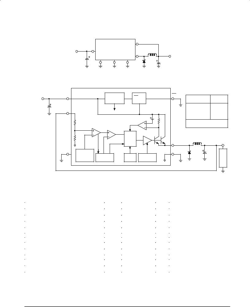
Figure 1. Block Diagram and Typical Application
Typical Application (Fixed Output Voltage Versions) |
||||||||
|
|
|
|
|
|
Feedback |
|
|
7.0 ± 40 V |
+Vin |
|
LM2574 |
|
1 |
L1 |
|
|
Unregulated |
5 |
|
|
|
|
Output |
330 μH |
5.0 V Regulated |
DC Input |
|
|
|
|
|
|||
Cin |
|
|
|
|
|
7 |
D1 |
Output 0.5 A Load |
22 μF |
|
|
|
|
|
Cout |
||
2 |
Sig |
4 |
Pwr |
3 |
ON/OFF |
1N5819 |
||
|
|
Gnd |
|
Gnd |
|
|
|
220 μF |
|
|
|
|
|
|
|
||
Representative Block Diagram and Typical Application
Unregulated |
+Vin |
|
|
3.1 V Internal |
ON/OFF |
ON/OFF |
Output |
|
R2 |
|
DC Input |
5 |
|
|
Regulator |
|
Voltage Versions |
(Ω) |
|||
|
|
|
|
3 |
||||||
|
|
|
|
|
|
|
|
1.7 k |
||
|
Cin |
|
|
|
|
|
|
3.3 V |
|
|
|
1 |
|
|
|
|
|
|
5.0 V |
|
3.1 k |
|
|
|
|
|
|
|
12 V |
|
8.84 k |
|
|
|
|
|
|
|
|
|
|
||
|
Feedback |
|
|
|
Current |
|
|
15 V |
|
11.3 k |
|
|
|
|
|
|
|
For adjustable version |
|
||
|
|
R2 |
Fixed Gain |
|
Limit |
|
|
|
||
|
|
|
Error Amplifier Comparator |
|
|
|
R1 = open, R2 = 0 Ω |
|
||
|
|
|
|
|
|
|
|
|
||
|
|
R1 |
|
|
|
Driver |
|
|
|
|
|
|
Freq |
|
Latch |
|
|
|
|
|
|
|
|
1.0 k |
|
|
Output |
L1 |
|
Vout |
||
|
|
Shift |
|
|
|
|
||||
|
|
|
|
|
|
|
|
|||
|
|
|
18 kHz |
|
|
1.0 Amp |
7 |
|
|
|
|
Sig Gnd |
1.235 V |
|
|
|
|
|
|||
|
|
|
Switch |
Pwr Gnd |
D1 |
Cout |
|
|||
|
|
52 kHz |
|
|
||||||
|
2 |
Band±Gap |
Reset |
Thermal |
4 |
|
|
Load |
||
|
Reference |
Oscillator |
Shutdown |
|
|
|||||
|
|
|
|
|
|
|||||
ABSOLUTE MAXIMUM RATINGS (Absolute Maximum Ratings indicate limits beyond which damage to the device may occur).
|
|
Rating |
Symbol |
Value |
Unit |
|
|
|
|
|
|
|
Maximum Supply Voltage |
Vin |
45 |
V |
|
|
ON/OFF Pin Input Voltage |
± |
±0.3 V ≤ V ≤ +Vin |
V |
|
|
Output Voltage to Ground (Steady State) |
± |
±1.0 |
V |
|
|
|
|
|
|
|
|
Power Dissipation |
PD |
Internally Limited |
W |
|
|
Thermal Resistance, Junction±to±Ambient |
RθJA |
100 |
°C/W |
|
|
Thermal Resistance, Junction±to±Case |
RθJC |
5.0 |
°C/W |
|
|
Storage Temperature Range |
Tstg |
±65°C to +150°C |
°C |
|
|
Minimum ESD Rating |
± |
2.0 |
kV |
|
|
(Human Body Model: C = 100 pF, R = 1.5 kΩ) |
|
|
|
|
|
|
|
|
|
|
|
Lead Temperature (Soldering, 10 seconds) |
± |
260 |
°C |
|
|
|
|
|
|
|
|
Maximum Junction Temperature |
TJ |
150 |
°C |
|
NOTE: ESD data available upon request.
2 |
MOTOROLA ANALOG IC DEVICE DATA |

LM2574
OPERATING RATINGS (Operating Ratings indicate conditions for which the device is intended to be functional, but do not guarantee specific performance limits. For guaranteed specifications and test conditions, see the Electrical Characteristics).
Rating |
Symbol |
Value |
Unit |
|
|
|
|
Operating Junction Temperature Range |
TJ |
±40 to +125 |
°C |
Supply Voltage |
Vin |
40 |
V |
SYSTEM PARAMETERS ([Note 1] Test Circuit Figure 16)
ELECTRICAL CHARACTERISTICS (Unless otherwise specified, Vin = 12 V for the 3.3 V, 5.0 V, and Adjustable version,
Vin = 25 V for the 12 V version, Vin = 30 V for the 15 V version. ILoad = 100 mA. For typical values TJ = 25°C, for min/max values TJ is the operating junction temperature range that applies [Note 2], unless otherwise noted).
Characteristic |
Symbol |
Min |
Typ |
Max |
Unit |
|
|
|
|
|
|
LM2574±3.3 ([Note 1] Test Circuit Figure 16) |
|
|
|
|
|
|
|
|
|
|
|
Output Voltage (Vin = 12 V, ILoad = 100 mA, TJ = 25°C) |
Vout |
3.234 |
3.3 |
3.366 |
V |
Output Voltage (4.75 V ≤ Vin ≤ 40 V, 0.1 A ≤ ILoad ≤ 0.5 A) |
Vout |
|
|
|
V |
TJ = 25°C |
|
3.168 |
3.3 |
3.432 |
|
TJ = ±40 to +125°C |
|
3.135 |
± |
3.465 |
|
Efficiency (Vin = 12 V, ILoad = 0.5 A) |
η |
± |
72 |
± |
% |
LM2574±5 ([Note 1] Test Circuit Figure 16) |
|
|
|
|
|
|
|
|
|
|
|
Output Voltage (Vin = 12 V, ILoad = 100 mA, TJ = 25°C) |
Vout |
4.9 |
5.0 |
5.1 |
V |
Output Voltage (7.0 V ≤ Vin ≤ 40 V, 0.1 A ≤ ILoad ≤ 0.5 A) |
Vout |
|
|
|
V |
TJ = 25°C |
|
4.8 |
5.0 |
5.2 |
|
TJ = ±40 to +125°C |
|
4.75 |
|
5.25 |
|
Efficiency (Vin = 12 V, ILoad = 0.5 A) |
η |
± |
77 |
± |
% |
LM2574±12 ([Note 1] Test Circuit Figure 16) |
|
|
|
|
|
|
|
|
|
|
|
Output Voltage (Vin = 25 V, ILoad = 100 mA, TJ = 25°C) |
Vout |
11.76 |
10 |
12.24 |
V |
Output Voltage (15 V ≤ Vin ≤ 40 V, 0.1 A ≤ ILoad ≤ 0.5 A) |
Vout |
|
|
|
V |
TJ = 25°C |
|
11.52 |
12 |
12.48 |
|
TJ = ±40 to +125°C |
|
11.4 |
± |
12.6 |
|
Efficiency (Vin = 15 V, ILoad = 0.5 A) |
η |
± |
88 |
± |
% |
LM2574±15 ([Note 1] Test Circuit Figure 16) |
|
|
|
|
|
|
|
|
|
|
|
Output Voltage (Vin = 30 V, ILoad = 100 mA, TJ = 25°C) |
Vout |
14.7 |
15 |
15.3 |
V |
Output Voltage (18 V < Vin < 40 V, 0.1 A < ILoad < 0.5 A) |
Vout |
|
|
|
V |
TJ = 25°C |
|
14.4 |
15 |
15.6 |
|
TJ = ±40 to +125°C |
|
14.25 |
|
15.75 |
|
Efficiency (Vin = 18 V, ILoad = 0.5 A) |
η |
± |
88 |
± |
% |
LM2574 ADJUSTABLE VERSION ([Note 1] Test Circuit Figure 16) |
|
|
|
|
|
|
|
|
|
|
|
Feedback Voltage Vin = 12 V, ILoad = 100 mA, Vout = 5.0 V, TJ = 25°C |
VFB |
1.217 |
1.23 |
1.243 |
V |
Feedback Voltage 7.0 V ≤ Vin ≤ 40 V, 0.1 A ≤ ILoad ≤ 0.5 A, Vout = 5.0 V |
VFBT |
|
|
|
V |
TJ = 25°C |
|
1.193 |
1.23 |
1.267 |
|
TJ = ±40 to +125°C |
|
1.18 |
|
1.28 |
|
Efficiency (Vin = 12 V, ILoad = 0.5 A, Vout = 5.0 V) |
η |
± |
77 |
± |
% |
NOTES: 1. External components such as the catch diode, inductor, input and output capacitors can affect the switching regulator system performance. When the LM2574 is used as shown in the Figure 16 test circuit, the system performance will be as
shown in the system parameters section of the Electrical Characteristics.
2. Tested junction temperature range for the LM2574: Tlow = ±40°C Thigh = +125°C
MOTOROLA ANALOG IC DEVICE DATA |
3 |
|

LM2574
SYSTEM PARAMETERS ([Note 1] Test Circuit Figure 16)
ELECTRICAL CHARACTERISTICS (continued) (Unless otherwise specified, Vin = 12 V for the 3.3 V, 5.0 V, and Adjustable version,
Vin = 25 V for the 12 V version, Vin = 30 V for the 15 V version. ILoad = 100 mA. For typical values TJ = 25°C, for min/max values TJ is the operating junction temperature range that applies [Note 2], unless otherwise noted).
|
|
|
|
Characteristic |
Symbol |
Min |
Typ |
Max |
Unit |
||
|
|
|
|
|
|
|
|
|
|
||
ALL OUTPUT VOLTAGE VERSIONS |
|
|
|
|
|
||||||
|
|
|
|
|
|
|
|
|
|
||
|
Feedback Bias Current Vout = 5.0 V (Adjustable Version Only) |
Ib |
|
|
|
nA |
|||||
|
TJ = 25°C |
|
|
|
|
|
± |
25 |
100 |
|
|
|
TJ = ±40 to +125°C |
|
± |
± |
200 |
|
|||||
|
Oscillator Frequency (Note 3) |
fO |
|
|
|
kHz |
|||||
|
TJ = 25°C |
|
|
|
|
|
± |
52 |
± |
|
|
|
TJ = 0 to +125°C |
|
47 |
52 |
58 |
|
|||||
|
TJ = ±40 to +125°C |
|
42 |
± |
63 |
|
|||||
|
Saturation Voltage (Iout = 0.5 A, [Note 4]) |
Vsat |
|
|
|
V |
|||||
|
TJ = 25°C |
|
|
|
|
|
± |
1.0 |
1.2 |
|
|
|
TJ = ±40 to +125°C |
|
± |
± |
1.4 |
|
|||||
|
Max Duty Cycle (ªonº) [Note 5] |
DC |
93 |
98 |
± |
% |
|||||
|
|
|
|
|
|
|
|
|
|
||
|
Current Limit Peak Current (Notes 3 and 4) |
ICL |
|
|
|
A |
|||||
|
TJ = 25°C |
|
|
|
|
|
0.7 |
1.0 |
1.6 |
|
|
|
TJ = ±40 to +125°C |
|
0.65 |
± |
1.8 |
|
|||||
|
Output Leakage Current (Notes 6 and 7), TJ = 25°C |
IL |
|
|
|
mA |
|||||
|
Output = 0 V |
|
|
|
|
± |
0.6 |
2.0 |
|
||
|
Output = ± 1.0 V |
|
± |
10 |
30 |
|
|||||
|
|
|
|
|
|
|
|
|
|
||
|
Quiescent Current (Note 6) |
IQ |
|
|
|
mA |
|||||
|
TJ = 25°C |
|
|
|
|
|
± |
5.0 |
9.0 |
|
|
|
TJ = ±40 to +125°C |
|
± |
± |
11 |
|
|||||
|
Standby Quiescent Current (ON/OFF Pin = 5.0 V (ªoffº)) |
Istby |
|
|
|
μA |
|||||
|
TJ = 25°C |
|
|
|
|
|
± |
60 |
200 |
|
|
|
TJ = ±40 to +125°C |
|
± |
± |
400 |
|
|||||
|
ON/OFF Pin Logic Input Level |
|
|
|
|
V |
|||||
|
Vout = 0 V |
|
|
|
|
VIH |
|
|
|
|
|
|
TJ = 25°C |
|
|
|
|
2.2 |
1.4 |
± |
|
||
|
TJ = ±40 to +125°C |
|
2.4 |
± |
± |
|
|||||
|
Nominal Output Voltage |
VIL |
|
|
|
|
|||||
|
TJ = 25°C |
|
|
|
|
|
± |
1.2 |
1.0 |
|
|
|
TJ = ±40 to +125°C |
|
± |
± |
0.8 |
|
|||||
|
ON/OFF Pin Input Current |
|
|
|
|
μA |
|||||
|
ON/OFF P |
in |
= 5.0 V (ªoffº), T = 25°C |
I |
± |
15 |
30 |
|
|||
|
|
|
|
J |
IH |
|
|
|
|
||
|
ON/OFF P |
in |
= 0 V (ªonº), T = 25°C |
I |
± |
0 |
5.0 |
|
|||
|
|
|
|
J |
IL |
|
|
|
|
||
NOTES: 1. External components such as the catch diode, inductor, input and output capacitors can affect the switching regulator system performance. When the LM2574 is used as shown in the Figure 16 test circuit, the system performance will be as
shown in the system parameters section of the Electrical Characteristics.
2.Tested junction temperature range for the LM2574: Tlow = ±40°C Thigh = +125°C
3.The oscillator frequency reduces to approximately 18 kHz in the event of an output short or an overload which causes the regulated output voltage to drop approximately 40% from the nominal output voltage. This self protection feature lowers the average power dissipation of the IC by lowering the minimum duty cycle from 5% down to approximately 2%.
4.Output (Pin 2) sourcing current. No diode, inductor or capacitor connected to the output pin.
5.Feedback (Pin 4) removed from output and connected to 0 V.
6.Feedback (Pin 4) removed from output and connected to 12 V for the Adjustable, 3.3 V, and 5.0 V versions, and 25 V for the 12 V and 15 V versions, to force the output transistor OFF.
7.Vin = 40 V.
4 |
MOTOROLA ANALOG IC DEVICE DATA |
LM2574
TYPICAL PERFORMANCE CHARACTERISTICS (Circuit of Figure 16)
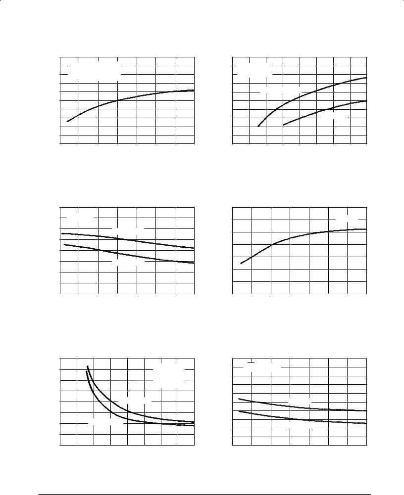
Figure 2. Normalized Output Voltage |
Figure 3. Line Regulation |
|
1.0 |
|
|
|
|
|
|
|
(%) |
0.8 |
Vin = 20 V |
|
|
|
|
|
|
CHANGE |
0.6 |
ILoad = 100 mA |
|
|
|
|
|
|
Normalized at TJ = 25°C |
|
|
|
|
||||
0.4 |
|
|
|
|
||||
|
|
|
|
|
|
|
||
|
|
|
|
|
|
|
|
|
VOLTAGE |
0.2 |
|
|
|
|
|
|
|
0 |
|
|
|
|
|
|
|
|
±0.2 |
|
|
|
|
|
|
|
|
, OUTPUT |
|
|
|
|
|
|
|
|
±0.4 |
|
|
|
|
|
|
|
|
±0.6 |
|
|
|
|
|
|
|
|
out |
±0.8 |
|
|
|
|
|
|
|
V |
|
|
|
|
|
|
|
|
|
±1.0 |
±25 |
0 |
25 |
60 |
75 |
100 |
125 |
|
±50 |
|||||||
|
|
|
TJ, JUNCTION TEMPERATURE (°C) |
|
|
|||
|
1.4 |
|
|
|
|
|
|
|
|
(%) |
1.2 |
ILoad = 100 mA |
|
|
|
|
|
|
|
CHANGE |
|
|
|
|
|
|
|
||
1.0 |
TJ = 25°C |
|
|
|
|
|
|
|
|
0.8 |
|
|
|
|
|
|
|
|
|
|
|
3.3 V, 5.0 V and ADJ |
|
|
|
|
|||
VOLTAGE |
0.6 |
|
|
|
|
|
|||
|
|
|
|
|
|
|
|
||
0.4 |
|
|
|
|
|
|
|
|
|
0.2 |
|
|
|
|
|
|
|
|
|
OUTPUT |
|
|
|
|
|
12 V and 15 V |
|
|
|
0 |
|
|
|
|
|
|
|
||
|
|
|
|
|
|
|
|
||
±0.2 |
|
|
|
|
|
|
|
|
|
, |
|
|
|
|
|
|
|
|
|
|
|
|
|
|
|
|
|
|
|
out |
±0.4 |
|
|
|
|
|
|
|
|
V |
|
|
|
|
|
|
|
|
|
|
±0.6 |
5.0 |
10 |
15 |
20 |
25 |
30 |
35 |
40 |
|
0 |
||||||||
|
|
|
|
Vin, INPUT VOLTAGE (V) |
|
|
|||
Figure 4. Dropout Voltage |
Figure 5. Current Limit |
|
2.0 |
|
|
|
|
|
|
|
(V) |
|
L = 300 μH |
|
|
|
|
|
|
DIFFERENTIAL |
1.5 |
|
|
ILoad = 500 mA |
|
|
|
|
|
|
|
|
|
|
|||
1.0 |
|
|
|
|
|
|
|
|
± OUTPUT |
|
|
|
|
|
|
|
|
|
|
|
ILoad = 100 mA |
|
|
|
||
0.5 |
|
|
|
|
|
|
|
|
INPUT |
|
|
|
|
|
|
|
|
|
|
|
|
|
|
|
|
|
|
0 |
±25 |
0 |
25 |
60 |
75 |
100 |
125 |
|
±50 |
|||||||
|
|
|
TJ, JUNCTION TEMPERATURE (°C) |
|
|
|||
|
1.4 |
|
|
|
|
|
|
|
(A) |
1.3 |
|
|
|
|
|
Vin = 25 V |
|
|
|
|
|
|
|
|
|
|
CURRENT |
1.2 |
|
|
|
|
|
|
|
1.1 |
|
|
|
|
|
|
|
|
|
|
|
|
|
|
|
|
|
, OUTPUT |
1.0 |
|
|
|
|
|
|
|
0.9 |
|
|
|
|
|
|
|
|
O |
|
|
|
|
|
|
|
|
I |
|
|
|
|
|
|
|
|
|
0.8 |
|
|
|
|
|
|
|
|
0.7 |
|
|
|
|
|
|
|
|
±50 |
±25 |
0 |
25 |
60 |
75 |
100 |
125 |
|
|
|
TJ, JUNCTION TEMPERATURE (°C) |
|
|
|||
Figure 6. Quiescent Current |
Figure 7. Standby Quiescent Current |
|
20 |
|
|
|
|
|
|
|
A) |
|
|
|
|
|
|
|
|
(μ |
|
|
|
|
|
|
|
|
Vout = 5.0 V |
||
QUIESCENTCURRENT (mA) |
18 |
|
|
|
|
|
QUIESCENT CURRENT |
||
|
|
|
|
|
|
Measured at |
|||
16 |
|
|
|
|
|
Ground Pin |
|||
14 |
|
|
|
|
|
TJ = 25°C |
|
||
|
|
|
|
|
|
|
|||
12 |
|
|
|
ILoad = 500 A |
|
|
|||
10 |
|
|
|
|
|
|
|
||
8.0 |
|
ILoad = 100 mA |
|
|
|
||||
, |
|
|
|
|
|
|
|
|
STANDBY, |
Q |
6.0 |
|
|
|
|
|
|
|
|
I |
|
|
|
|
|
|
|
||
|
4.0 |
|
|
|
|
|
|
|
stby |
|
|
|
|
|
|
|
|
I |
|
|
0 |
5.0 |
10 |
15 |
20 |
25 |
30 |
35 |
40 |
|
|
|
|
Vin, INPUT VOLTAGE (V) |
|
|
|
||
200 |
|
|
|
|
|
|
|
180 |
VON/OFF = 5.0 V |
|
|
|
|
|
|
160 |
|
|
|
|
|
|
|
140 |
|
|
|
|
|
|
|
120 |
|
|
|
|
|
|
|
100 |
|
|
Vin = 40 V |
|
|
|
|
80 |
|
|
|
|
|
|
|
60 |
|
|
Vin = 12 V |
|
|
|
|
40 |
|
|
|
|
|
||
|
|
|
|
|
|
|
|
20 |
|
|
|
|
|
|
|
0 |
|
|
|
|
|
|
|
±50 |
±25 |
0 |
25 |
60 |
75 |
100 |
125 |
|
|
TJ, JUNCTION TEMPERATURE (°C) |
|
|
|||
MOTOROLA ANALOG IC DEVICE DATA |
5 |
|

LM2574
TYPICAL PERFORMANCE CHARACTERISTICS (Circuit of Figure 16) (continued)
Figure 8. Oscillator Frequency
|
8.0 |
|
|
|
|
|
|
|
(%) |
6.0 |
Vin = 12 V |
|
|
|
|
|
|
4.0 |
Normalized at 25°C |
|
|
|
|
|
||
FREQUENCY |
|
|
|
|
|
|||
|
|
|
|
|
|
|
||
2.0 |
|
|
|
|
|
|
|
|
0 |
|
|
|
|
|
|
|
|
±2.0 |
|
|
|
|
|
|
|
|
NORMALIZED |
|
|
|
|
|
|
|
|
±4.0 |
|
|
|
|
|
|
|
|
±6.0 |
|
|
|
|
|
|
|
|
±8.0 |
|
|
|
|
|
|
|
|
|
|
|
|
|
|
|
|
|
|
10 |
±25 |
0 |
25 |
50 |
75 |
100 |
125 |
|
±50 |
|||||||
|
|
|
TJ, JUNCTION TEMPERATURE (°C) |
|
|
|||
Figure 10. Minimum Operating Voltage
|
5.0 |
|
|
|
|
|
|
|
|
4.5 |
|
|
|
Adjustable Version Only |
|
||
(V) |
4.0 |
|
|
|
|
|
|
|
3.5 |
|
|
|
|
|
|
|
|
VOLTAGE |
|
|
|
|
|
|
|
|
3.0 |
|
|
|
|
|
|
|
|
2.5 |
|
|
|
|
|
|
|
|
,INPUT |
|
|
|
|
|
|
|
|
2.0 |
|
|
|
|
|
|
|
|
1.5 |
|
|
|
|
|
|
|
|
in |
Vin = 1.23 V |
|
|
|
|
|
||
|
|
|
|
|
|
|||
V |
1.0 |
|
|
|
|
|
||
|
|
|
|
|
|
|||
|
ILoad = 100 mA |
|
|
|
|
|
||
|
0.5 |
|
|
|
|
|
||
|
|
|
|
|
|
|
|
|
|
0 |
±25 |
0 |
25 |
50 |
75 |
100 |
125 |
|
±50 |
|||||||
|
|
|
TJ, JUNCTION TEMPERATURE (°C) |
|
|
|||
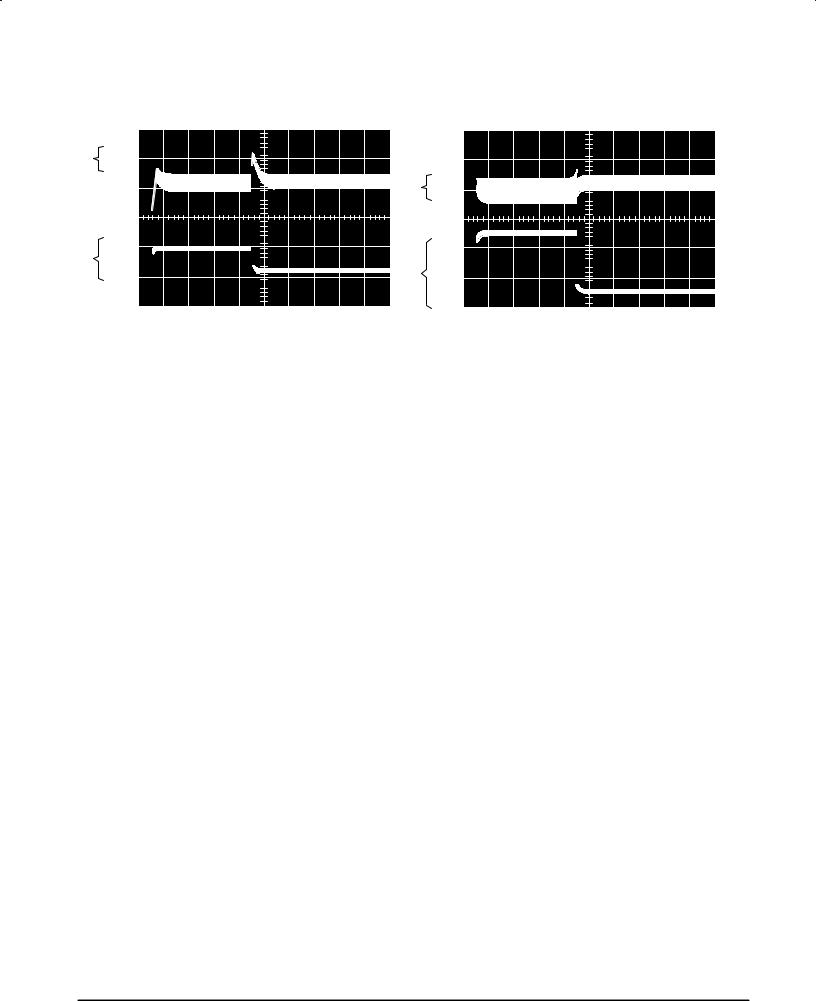
Figure 12. Continuous Mode Switching Waveforms Vout = 5.0 V, 500 mA Load Current, L = 330 μH
|
20 V |
|
A |
10 V |
|
|
0 |
|
|
0.6 A |
|
B |
0.4 A |
|
|
||
|
0.2 A |
|
|
0 |
|
C |
20 mV |
|
AC |
||
|
||
|
5 μs/DIV |
A:Output Pin Voltage, 10 V/DIV.
B:Inductor Current, 0.2 A/DIV.
C:Output Ripple Voltage, 20 mV/DIV, AC±Coupled
Figure 9. Switch Saturation Voltage
|
1.3 |
|
|
|
|
|
(V) |
1.2 |
|
|
|
|
|
1.1 |
|
|
|
|
|
|
VOLTAGE |
|
|
|
|
|
|
1.0 |
|
|
|
|
|
|
0.9 |
±40°C |
|
|
|
|
|
, SATURATION |
|
|
|
|
||
0.8 |
25°C |
|
|
|
|
|
0.7 |
|
|
|
|
|
|
0.6 |
125°C |
|
|
|
|
|
0.5 |
|
|
|
|
|
|
sat |
|
|
|
|
|
|
|
|
|
|
|
|
|
V |
0.4 |
|
|
|
|
|
|
|
|
|
|
|
|
|
0.3 |
|
|
|
|
|
|
0 |
0.1 |
0.2 |
0.3 |
0.4 |
0.5 |
SWITCH CURRENT (A)
|
100 |
Figure 11. Feedback Pin Current |
|
|||||
(nA) |
|
|
|
|
|
|
|
|
80 |
|
|
|
Adjustable Version Only |
|
|||
CURRENT |
|
|
|
|
||||
20 |
|
|
|
|
|
|
|
|
|
60 |
|
|
|
|
|
|
|
|
40 |
|
|
|
|
|
|
|
PIN |
0 |
|
|
|
|
|
|
|
FEEDBACK, |
|
|
|
|
|
|
|
|
±60 |
|
|
|
|
|
|
|
|
|
±20 |
|
|
|
|
|
|
|
|
±40 |
|
|
|
|
|
|
|
FB |
±80 |
|
|
|
|
|
|
|
I |
|
|
|
|
|
|
|
|
|
±100 |
±25 |
0 |
25 |
50 |
75 |
100 |
125 |
|
±50 |
|||||||
TJ, JUNCTION TEMPERATURE (°C)
Figure 13. Discontinuous Mode Switching Waveforms Vout = 5.0 V, 100 mA Load Current, L = 100 μH
|
20 V |
|
A |
10 V |
|
|
0 |
|
|
0.6 A |
|
B |
0.4 A |
|
|
0.2 A |
|
|
0 |
|
C |
20 mV |
|
AC |
||
|
||
|
5 μs/DIV |
A:Output Pin Voltage, 10 V/DIV.
B:Inductor Current, 0.2 A/DIV.
C:Output Ripple Voltage, 20 mV/DIV, AC±Coupled
6 |
MOTOROLA ANALOG IC DEVICE DATA |
LM2574
TYPICAL PERFORMANCE CHARACTERISTICS (Circuit of Figure 16) (continued)
Figure 14. 500 mA Load Transient Response for Continuous Mode Operation, L = 330 μH, Cout = 300 μF
A |
50 mV |
|
AC |
||
|
||
B |
500 mA |
|
|
||
|
0 |
|
|
200 μs/DIV |
Figure 15. 250 mA Load Transient Response for Discontinuous Mode Operation, L = 68 μH, Cout = 470 μF
A |
50 mV |
|
AC |
||
|
||
|
200 mA |
|
B |
100 mA |
|
|
||
|
0 |
|
|
200 μs/DIV |
A: Output Voltage, 50 mV/DIV, AC Coupled |
A: Output Voltage, 50 mV/DIV, AC Coupled |
B: 100 mA to 500 mA Load Pulse |
B: 50 mA to 250 mA Load Pulse |
MOTOROLA ANALOG IC DEVICE DATA |
7 |
|
LM2574
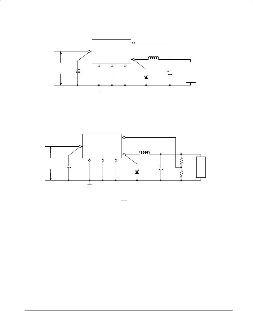
Figure 16. Test Circuit and Layout Guidelines
Fixed Output Voltage Versions
|
|
|
|
|
|
Feedback |
|
|
|
|
|
Vin |
|
LM2574 |
1 |
|
|
|
|
|
|
|
L1 |
|
|
||||
|
|
|
|
Fixed Output |
330 |
μ |
|
|
|
|
|
1 |
|
|
|
H |
|
|
|
|
|
|
|
|
Output |
|
|
Vout |
|
|
|
|
|
|
|
|
|
||
7.0 ± 40 V |
|
|
|
|
|
7 |
|
|
|
|
|
|
4 Pwr 2 |
Sig 3 |
ON/OFF |
|
|
|
|
Unregulated |
|
|
|
|
|
|
|||
Cin |
|
Gnd |
Gnd |
|
|
|
|
||
DC Input |
|
|
Cout |
Load |
|||||
|
|
|
D1 |
||||||
|
22 |
μF |
|
|
|
220 |
μF |
|
|
|
|
|
|
|
|
1N5819 |
|
|
|
|
|
Cin |
± |
22 μF, 60 V, Aluminium Electrolytic |
|
|
|
||
|
|
Cout ± |
220 μF, 25 V, Aluminium Electrolytic |
|
|
|
|||
|
|
D1 |
± |
Schottky, 1N5819 |
|
|
|
|
|
|
|
L1 |
± |
330 μH, (For 5.0 Vin, 3.3 Vout, use 100 μH) |
|
|
|
||
|
|
R1 |
± |
2.0 k, 0.1% |
|
|
|
|
|
|
|
R2 |
± |
6.12 k, 0.1% |
|
|
|
|
|
|
|
|
Adjustable Output Voltage Versions |
|
|
||||||||
|
|
|
|
|
|
|
|
Feedback |
|
|
|
||
|
|
Vin |
LM2574 |
|
|
1 |
|
|
|
|
|
||
|
|
|
|
|
|
|
L1 |
|
Vout |
||||
|
|
1 |
Adjustable |
|
|
Output |
|
330 μH |
|
||||
|
|
|
|
|
|
|
|
|
|
|
5.0 V |
||
7.0 V ± 40 V |
|
|
|
|
|
|
|
7 |
|
|
|
|
R2 |
|
4 |
Pwr |
2 |
Sig |
3 |
ON/OFF |
|
|
|
|
|||
Unregulated |
|
|
|
|
|
6.12 k |
|||||||
Cin |
Gnd |
|
Gnd |
|
|
|
|
|
|
|
|||
DC Input |
|
|
|
|
|
|
|
Cout |
Load |
||||
|
|
|
|
|
|
|
|
D1 |
|||||
|
22 |
μF |
|
|
|
|
|
|
|
|
220 μF |
R1 |
|
|
|
|
|
|
|
|
|
|
|
|
1N5819 |
|
|
|
|
|
|
|
|
|
|
|
|
|
|
2.0 k |
|
|
|
|
|
|
|
|
|
|
|
|
|
|
|
|
|
|
|
|
Vout + Vref 1.0 ) |
R2 |
|
|
|
||||
|
|
|
|
|
R1 |
|
|
|
|||||
|
|
|
|
|
|
|
|
|
|
|
|
|
|
|
|
|
|
|
R2 + R1 |
Vout |
± 1.0 |
|
|
||||
|
|
|
|
|
Vref |
|
|
||||||
|
|
|
|
|
|
|
|
|
|
|
|
|
|
|
|
|
|
|
Where Vref = 1.23 V, R1 |
|
|
|
|||||
|
|
|
|
|
between 1.0 kΩ and 5.0 kΩ |
|
|
||||||
PCB LAYOUT GUIDELINES
As in any switching regulator, the layout of the printed circuit board is very important. Rapidly switching currents associated with wiring inductance, stray capacitance and parasitic inductance of the printed circuit board traces can generate voltage transients which can generate electromagnetic interferences (EMI) and affect the desired operation. As indicated in the Figure 16, to minimize inductance and ground loops, the length of the leads indicated by heavy lines should be kept as short as possible.
For best results, single±point grounding (as indicated) or ground plane construction should be used.
On the other hand, the PCB area connected to the Pin 7 (emitter of the internal switch) of the LM2574 should be kept to a minimum in order to minimize coupling to sensitive circuitry.
Another sensitive part of the circuit is the feedback. It is important to keep the sensitive feedback wiring short. To assure this, physically locate the programming resistors near to the regulator, when using the adjustable version of the LM2574 regulator.
8 |
MOTOROLA ANALOG IC DEVICE DATA |
 Loading...