


74ACT04SCX
Fairchild Semiconductor 74ACT04SCX, 74ACT04SC, 74ACT04PC, 74ACT04MTCX, 74ACT04MTC Datasheet
...
© 1999 Fairchild Semiconductor Corporation DS009913 www.fairchildsemi.com
November 1988
Revised November 1999
74AC04 • 74ACT04 Hex Inverter
74AC04 • 74ACT04
Hex Inverter
General Description
The AC/ACT04 contains six inverters.
Features
■ I
CC
reduced by 50% on 74AC only
■ Outputs source/sink 24 mA
■ ACT04 has TTL-compatible inputs
Ordering Code:
Device also available in Tape and Reel. Specify by appending suffix letter “X” to the ordering code. (PC not available in Tape and Reel.)
Logic Symbol
IEEE/IEC
Connection Diagram
Pin Descriptions
FACT is a trademark of Fairchild Semiconductor Corporation.
Order Number Package Number Package Description
74AC04SC M14A 14-Lead Small Outline Integrated Circuit (SOIC), JEDEC MS-120, 0.150” Narrow Body
74AC04SJ M14D 14-Lead Small Outline Package (SOP), EIAJ TYPE II, 5.3mm Wide
74AC04MTC MTC14 14-Lead Thin Shrink Small Outline Package (TSSOP), JEDEC MO-153, 4.4mm Wide
74AC04PC N14A 14-Lead Plastic Dual-In-Line Package (PDIP), JEDEC MS-001, 0.300” Wide
74ACT04SC M14A 14-Lead Small Outline Integrated Circuit (SOIC), JEDEC MS-120, 0.150” Narrow Body
74ACT04MTC MTC14 14-Lead Thin Shrink Small Outline Package (TSSOP), JEDEC MO-153, 4.4mm Wide
74ACT04PC N14A 14-Lead Plastic Dual-In-Line Package (PDIP), JEDEC MS-001, 0.300” Wide
Pin Names Description
A
n
Inputs
O
n
Outputs

www.fairchildsemi.com 2
74AC04 • 74ACT04
Absolute Maximum Ratings(Note 1) Recommended Operating
Conditions
Note 1: Absolute maximum ratings are those values beyond which damage
to the device may occur. The databook specifications should be met, with-
out exception, to ensure that the system design is reliable over its power
supply, temperature, and ou tput/inp ut loadi ng varia bles. Fairchild does no t
recommend operat ion of FACT circuits outside da t abook specifications.
DC Electrical Characteristics for AC
Note 2: All outputs loaded; thresholds on input assoc iat ed with output under tes t.
Note 3: Maximum test duratio n 2. 0 ms, one output loaded at a time.
Note 4: I
IN
and I
CC
@ 3.0V are guaranteed to be less than or equa l to th e respective limit @ 5.5V V
CC
.
Supply Voltage (V
CC
) −0.5V to +7.0V
DC Input Diode Current (I
IK
)
V
I
= −0.5V −20 mA
V
I
= V
CC
+ 0.5V +20 mA
DC Input Voltage (V
I
) −0.5V to V
CC
+ 0.5V
DC Output Diode Current (I
OK
)
V
O
= −0.5V −20 mA
V
O
= V
CC
+ 0.5V +20 mA
DC Output Voltage (V
O
)
−0.5V toV
CC
+ 0.5V
DC Output Source or Sink Current (I
O
) ±50 mA
DC V
CC
or Ground Current
per Output Pin (I
CC
or I
GND
) ±50 mA
Storage Temperature (T
STG
) −65°C to +150°C
Junction Temperature (T
J
)
PDIP 140°C
Supply Voltage (V
CC
)
AC 2.0V to 6.0V
ACT 4.5V to 5.5V
Input Voltage (V
I
) 0V to V
CC
Output Voltage (V
O
) 0V to V
CC
Operating Temperature (T
A
) −40°C to +85°C
Minimum Input Edge Rate (∆V/∆t)
AC Devices
V
IN
from 30% to 70% of V
CC
V
CC
@ 3.3V, 4.5V, 5.5V 125 mV/ns
Minimum Input Edge Rate (∆V/∆t)
ACT Devices
V
IN
from 0.8V to 2.0V
V
CC
@ 4.5V, 5.5V 125 mV/ns
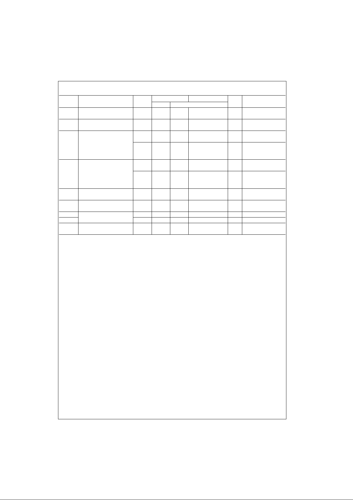
Symbol Parameter
V
CC
T
A
= +25°C
T
A
= −40°C to +85°C
Units Conditions
(V) Typ Guaranteed Limits
V
IH
Minimum HIGH Level 3.0 1.5 2.1 2.1 V
OUT
= 0.1V
Input Voltage 4.5 2.25 3.15 3.15 V or V
CC
− 0.1V
5.5 2.75 3.85 3.85
V
IL
Maximum LOW Level 3.0 1.5 0.9 0.9 V
OUT
= 0.1V
Input Voltage 4.5 2.25 1.35 1.35 V or V
CC
− 0.1V
5.5 2.75 1.65 1.65
V
OH
Minimum HIGH Level 3.0 2.99 2.9 2.9
Output Voltage 4.5 4.49 4.4 4.4 V I
OUT
= −50 µA
5.5 5.49 5.4 5.4
V
IN
= V
IL
or V
IH
3.0 2.56 2.46 I
OH
= −12 mA
4.5 3.86 3.76 V I
OH
= −24 mA
5.5 4.86 4.76 I
OH
= −24 mA (Note 2)
V
OL
Maximum LOW Level 3.0 0.002 0.1 0.1
Output Voltage 4.5 0.001 0.1 0.1 V I
OUT
= 50 µA
5.5 0.001 0.1 0.1
V
IN
= V
IL
or V
IH
3.0 0.36 0.44 I
OL
= 12 mA
4.5 0.36 0.44 V I
OL
= 24 mA
5.5 0.36 0.44 I
OL
= 24 mA (Note 2)
I
IN
Maximum Input
5.5 ±0.1 ±1.0 µAV
I
= V
CC
, GND
(Note 4) Leakage Current
I
OLD
Minimum Dynamic Output Current 5.5 75 mA V
OLD
= 1.65V Max
I
OHD
(Note 3) 5.5 −75 mA V
OHD
= 3.85V Min
I
CC
Maximum Quiescent
5.5 2.0 20.0 µA
V
IN
= V
CC
(Note 4) Supply Current or GND
3 www.fairchildsemi.com
74AC04 • 74ACT04
DC Electrical Characteristics for ACT
Note 5: All outputs loaded; thres holds on input associate d w it h output under test.
Note 6: Maximum test duration 2.0 ms, one output loaded at a time.
Symbol Parameter
V
CC
T
A
= +25°CT
A
= −40°C to +85°C
Units Conditions
(V) Typ Guaranteed Limits
V
IH
Minimum HIGH Level 4.5 1.5 2.0 2.0
V
V
OUT
= 0.1V
Input Voltage 5.5 1.5 2.0 2.0 or V
CC
− 0.1V
V
IL
Maximum LOW Level 4.5 1.5 0.8 0.8
V
V
OUT
= 0.1V
Input Voltage 5.5 1.5 0.8 0.8 or V
CC
− 0.1V
V
OH
Minimum HIGH Level 4.5 4.49 4.4 4.4
VI
OUT
= −50 µA
Output Voltage 5.5 5.49 5.4 5.4
V
IN
= V
IL
or V
IH
4.5 3.86 3.76
V
I
OH
= −24 mA
5.5 4.86 4.76 I
OH
= −24 mA (Note 5)
V
OL
Maximum LOW Level 4.5 0.001 0.1 0.1
VI
OUT
= 50 µA
Output Voltage 5.5 0.001 0.1 0.1
V
IN
= V
IL
or V
IH
4.5 0.36 0.44
V
I
OL
0 = 24 mA
5.5 0.36 0.44 I
OL
= 24 mA (Note 5)
I
IN
Maximum Input
5.5 ±0.1 ±1.0 µAV
I
= V
CC
, GND
Leakage Current
I
CCT
Maximum
5.5 0.6 1.5 mA V
I
= V
CC
− 2.1V
I
CC
/Input
I
OLD
Minimum Dynamic Output Current 5.5 75 mA V
OLD
= 1.65V Max
I
OHD
(Note 6) 5.5 −75 mA V
OHD
= 3.85V Min
I
CC
Maximum Quiescent
5.5 4.0 40.0 µA
V
IN
= V
CC
Supply Current or GND
 Loading...