


 Loading...
a Dual, 12-Bit, 40 MSPS MCM A/D Converter with Analog Input Signal Conditioning
AD10242
FEATURES
Two Matched ADCs with Input Signal Conditioning Selectable Bipolar Input Voltage Range
( 0.5 V, 1.0 V, 2.0 V)
Full MIL-STD-883B Compliant
80 dB Spurious-Free Dynamic Range
Trimmed Channel-Channel Matching
APPLICATIONS
Radar Processing
Communications Receivers
FLIR Processing
Secure Communications
Any I/Q Signal Processing Application
PRODUCT DESCRIPTION
The AD10242 is a complete dual signal chain solution including onboard amplifiers, references, ADCs, and output buffering providing unsurpassed total system performance. Each channel is laser trimmed for gain and offset matching and provides channel- to-channel crosstalk performance better than 80 dB. The AD10242 utilizes two each of the AD9632, OP279, and AD9042 in a custom MCM to gain space, performance, and cost advantages over solutions previously available.
The AD10242 operates with ±5.0 V for the analog signal conditioning with a separate 5.0 V supply for the analog-to-digital conversion. Each channel is completely independent, allowing operation with independent encode or analog inputs. The AD10242 also offers the user a choice of analog input signal ranges to minimize additional signal conditioning required for multiple functions within a single system. The heart of the AD10242 is the AD9042, which is designed specifically for applications requiring wide dynamic range.
The AD10242 is manufactured by Analog Devices on our MIL-PRF-38534 MCM line and is completely qualified. Units
are packaged in a custom cofired ceramic 68-lead gull wing package and specified for operation from –55°C to +125°C.
Contact the factory for additional custom options including those which allow the user to ac couple the ADC directly, bypassing the front end amplifier section. Also see the AD9042 data sheet for additional details on ADC performance.
PRODUCT HIGHLIGHTS
1.Guaranteed sample rate of 40 MSPS.
2.Dynamic performance specified over entire Nyquist band; spurious signals @ 80 dBc for –1 dBFS input signals.
3.Low power dissipation: <2 W off ± 5.0 V supplies.
4.User defined input amplitude.
5.Packaged in 68-lead ceramic leaded chip carrier.
FUNCTIONAL BLOCK DIAGRAM
|
AIN3 |
|
AIN2 |
AIN1 |
UNEG |
UCOM |
UPOS |
AIN3 |
|
AIN2 |
AIN1 |
|
|
UPOS |
|
|
|
|
|
|
|
|
|
|
|
|
|
|
|
OP279 |
AD9632 |
|
|
|
|
OP279 |
|
AD9632 |
|
||
|
|
|
|
|
|
|
|
|
|
|
|
||
UCOM |
|
|
|
|
|
|
|
|
|
|
|
|
|
UNEG |
|
|
|
|
|
|
|
|
|
|
|
|
|
(LSB) D0A |
|
OP279 |
AD9042 |
|
|
OP279 |
|
AD9042 |
|
|
ENC |
||
|
|
|
|
|
|
|
|
|
|
|
TIMING |
||
|
|
|
|
|
|
|
|
|
|
|
|
||
D1A |
|
|
|
VREF |
|
|
|
|
|
|
VREF |
|
ENC |
|
|
|
|
|
|
|
|
|
|
|
|||
D2A |
|
|
|
|
|
|
|
|
|
|
|
||
|
|
|
|
|
|
|
|
|
|
|
|
|
|
D3A |
|
|
|
12 |
|
AD10242 |
|
|
|
12 |
|
D11B (MSB) |
|
|
|
|
|
|
|
|
|
|
|||||
|
9 |
|
|
|
|
|
|
|
D10B |
||||
D4A |
|
|
|
|
|
|
|
|
|
|
|
||
|
OUTPUT BUFFERING |
|
|
|
|
|
|
|
|
5 |
|||
|
|
|
|
|
|
|
|
|
|
|
|||
D5A |
|
|
|
|
|
|
|
OUTPUT BUFFERING |
D9B |
||||
|
|
|
|
|
|
|
|
|
|||||
|
|
|
|
|
|
|
|
|
|
|
|
|
|
D6A |
|
|
|
|
|
|
|
|
|
|
|
|
D8B |
|
|
|
|
|
|
|
|
|
|
7 |
|
|
|
D7A |
|
|
|
|
|
|
|
|
|
|
|
D7B |
|
TIMING |
|
|
|
|
|
|
|
|
|
|
|||
|
|
|
|
|
|
|
|
|
|
|
|||
|
|
|
|
|
|
|
|
|
|
|
|
||
D8A |
|
|
|
|
|
|
|
|
|
|
|
|
|
|
ENC |
ENC |
D9A |
D10A D11A |
|
|
D0B |
D1B |
D2B |
D3B |
D4B |
D5B |
D6B |
|
|
|
|
(MSB) |
|
|
(LSB) |
|
|
|
|
|
|
REV. B
Information furnished by Analog Devices is believed to be accurate and reliable. However, no responsibility is assumed by Analog Devices for its use, nor for any infringements of patents or other rights of third parties that may result from its use. No license is granted by implication or otherwise under any patent or patent rights of Analog Devices.
One Technology Way, P.O. Box 9106, Norwood, MA 02062-9106, U.S.A.
Tel: 781/329-4700 |
www.analog.com |
Fax: 781/326-8703 |
© Analog Devices, Inc., 2001 |
AD10242–SPECIFICATIONS
Electrical Characteristics |
(AVCC = 5 V; AVEE = –5.0 V; DVCC = 5 V; applies to each ADC unless otherwise noted.) |
|
|||||||
|
|
|
|
Test |
Mil |
|
AD10242BZ/TZ |
|
|
Parameter |
|
|
Temp |
Level |
Subgroup |
Min |
Typ |
Max |
Unit |
|
|
|
|
|
|
|
|
|
|
RESOLUTION |
|
|
|
|
|
|
12 |
|
Bits |
|
|
|
|
|
|
|
|
|
|
DC ACCURACY |
|
|
|
|
|
|
|
|
|
No Missing Codes |
|
Full |
VI |
1, 2, 3 |
|
Guaranteed |
|
|
|
Offset Error |
|
|
25°C |
I |
1 |
–0.5 |
±0.05 |
+0.5 |
% FS |
|
|
|
Full |
VI |
2, 3 |
–2.0 |
±1.0 |
+2.0 |
% FS |
Offset Error Channel Match |
|
Full |
V |
|
|
±0.1 |
|
% |
|
Gain Error1 |
|
|
25°C |
I |
1 |
–1.0 |
±0.5 |
+1.0 |
% FS |
|
|
|
Full |
VI |
2, 3 |
–1.5 |
±0.8 |
+1.5 |
% FS |
Gain Error Channel Match |
|
Full |
V |
|
|
±0.1 |
|
% |
|
|
|
|
|
|
|
|
|
|
|
ANALOG INPUT (AIN) |
|
|
|
|
|
|
|
|
|
Input Voltage Range |
|
|
|
|
|
±0.5 |
|
|
|
AIN1 |
|
|
Full |
I |
|
|
|
V |
|
AIN2 |
|
|
Full |
I |
|
|
±1.0 |
|
V |
AIN3 |
|
|
Full |
I |
|
|
±2 |
|
V |
Input Resistance |
|
|
|
|
|
|
|
Ω |
|
AIN1 |
|
|
Full |
IV |
12 |
99 |
100 |
101 |
|
AIN2 |
|
|
Full |
IV |
12 |
198 |
200 |
202 |
Ω |
AIN3 |
|
|
Full |
IV |
12 |
396 |
400 |
404 |
Ω |
Input Capacitance2 |
|
25°C |
IV |
12 |
0 |
4.0 |
7.0 |
pF |
|
Analog Input Bandwidth3 |
|
Full |
V |
|
|
60 |
|
MHz |
|
ENCODE INPUT4, 5 |
|
|
|
|
|
|
|
|
|
Logic Compatibility |
|
|
|
|
|
TTL/CMOS |
|
|
|
Logic “1” Voltage |
|
Full |
I |
1, 2, 3 |
2.0 |
|
5.0 |
V |
|
Logic “0” Voltage |
|
Full |
I |
1, 2, 3 |
0 |
|
0.8 |
V |
|
Logic “1” Current (VINH = 5 V) |
|
Full |
I |
1, 2, 3 |
|
625 |
800 |
µA |
|
Logic “0” Current (VINL = 0 V) |
|
Full |
I |
1, 2, 3 |
–400 |
–300 |
|
µA |
|
Input Capacitance |
|
25°C |
V |
12 |
|
|
7.0 |
pF |
|
|
|
|
|
|
|
|
|
|
|
SWITCHING PERFORMANCE |
|
|
|
|
|
|
|
|
|
Maximum Conversion Rate6 |
|
Full |
VI |
4, 5, 6 |
40 |
50 |
|
MSPS |
|
Minimum Conversion Rate6 |
|
Full |
V |
12 |
|
|
5 |
MSPS |
|
Aperture Delay (tA) |
|
25°C |
V |
|
|
1.0 |
|
ns |
|
Aperture Delay Matching |
|
25°C |
V |
|
|
±2.0 |
|
ns |
|
Aperture Uncertainty (Jitter) |
|
25°C |
V |
|
|
1 |
|
ps rms |
|
ENCODE Pulsewidth High |
|
25°C |
IV |
12 |
12 |
10 |
|
ns |
|
ENCODE Pulsewidth Low |
|
25°C |
IV |
12 |
|
10 |
41 |
ns |
|
Output Delay (tOD) |
|
Full |
IV |
12 |
10 |
12 |
14 |
ns |
|
SNR7 |
|
|
25°C |
|
|
|
|
|
|
Analog Input |
@ 1.2 MHz |
|
V |
|
|
68 |
|
dB |
|
|
@ 4.85 MHz |
|
25°C |
I |
4 |
63 |
66 |
|
dB |
|
|
|
Full |
II |
5, 6 |
62 |
66 |
|
dB |
|
@ 9.9 MHz |
|
25°C |
I |
4 |
63 |
65 |
|
dB |
|
|
|
Full |
II |
5, 6 |
62 |
65 |
|
dB |
|
@ 19.5 MHz |
|
25°C |
I |
4 |
60 |
63 |
|
dB |
|
|
|
Full |
II |
5, 6 |
59 |
62 |
|
dB |
|
|
|
|
|
|
|
|
|
|
SINAD8 |
|
|
25°C |
|
|
|
|
|
|
Analog Input |
@ 1.2 MHz |
|
V |
|
|
67 |
|
dB |
|
|
@ 4.85 MHz |
|
25°C |
I |
4 |
62 |
65 |
|
dB |
|
|
|
Full |
II |
5, 6 |
61 |
64 |
|
dB |
|
@ 9.9 MHz |
|
25°C |
I |
4 |
60 |
64 |
|
dB |
|
|
|
Full |
II |
5, 6 |
60 |
63 |
|
dB |
|
@ 19.5 MHz |
|
25°C |
I |
4 |
58 |
61 |
|
dB |
|
|
|
Full |
II |
5, 6 |
58 |
60 |
|
dB |
|
|
|
|
|
|
|
|
|
|
–2– |
REV. B |
|
|
|
|
|
|
|
AD10242 |
|
|
|
|
|
|
|
|
|
|
Test |
Mil |
|
AD10242BZ/TZ |
|
|
Parameter |
Temp |
Level |
Subgroup |
Min |
Typ |
Max |
Unit |
|
|
|
|
|
|
|
|
SPURIOUS-FREE DYNAMIC RANGE9 |
25°C |
|
|
|
|
|
|
Analog Input @ 1.2 MHz |
I |
|
|
81 |
|
dBFS |
|
@ 4.85 MHz |
25°C |
I |
4 |
70 |
80 |
|
dBFS |
|
Full |
II |
5, 6 |
70 |
79 |
|
dBFS |
@ 9.9 MHz |
25°C |
I |
4 |
63 |
70 |
|
dBFS |
|
Full |
II |
5, 6 |
63 |
69 |
|
dBFS |
@ 19.5 MHz |
25°C |
I |
4 |
60 |
67 |
|
dBFS |
|
Full |
II |
5, 6 |
60 |
66 |
|
dBFS |
|
|
|
|
|
|
|
|
TWO-TONE IMD REJECTION10 |
|
|
|
|
|
|
|
F1, F2 @ –7 dBFS |
Full |
II |
4, 5, 6 |
70 |
76 |
|
dBc |
|
|
|
|
|
|
|
|
CHANNEL-TO-CHANNEL ISOLATION11 |
25°C |
IV |
12 |
75 |
80 |
|
dB |
TRANSIENT RESPONSE |
25°C |
V |
|
|
10 |
|
ns |
|
|
|
|
|
|
|
|
LINEARITY |
25°C |
|
|
|
|
|
|
Differential Nonlinearity |
IV |
12 |
|
0.3 |
1.0 |
LSB |
|
(Encode = 20 MHz) |
Full |
IV |
12 |
|
0.5 |
1.25 |
LSB |
Integral Nonlinearity |
25°C |
V |
|
|
0.3 |
|
LSB |
(Encode = 20 MHz) |
Full |
V |
|
|
0.5 |
|
LSB |
|
|
|
|
|
|
|
|
OVERVOLTAGE RECOVERY TIME12 |
|
|
|
|
|
|
|
VIN = 2.0 × FS |
Full |
IV |
12 |
|
50 |
100 |
ns |
VIN = 4.0 × FS |
Full |
IV |
12 |
|
75 |
200 |
ns |
DIGITAL OUTPUTS |
|
|
|
|
|
|
|
Logic Compatibility |
|
|
|
|
CMOS |
|
|
Logic “1” Voltage13 |
Full |
I |
1, 2, 3 |
3.5 |
4.2 |
|
V |
Logic “0” Voltage14 |
Full |
I |
1, 2, 3 |
|
0.45 |
0.65 |
V |
Output Coding |
|
|
|
Two’s Complement |
|
|
|
|
|
|
|
|
|
|
|
POWER SUPPLY |
|
|
|
|
|
|
|
AVCC Supply Voltage |
Full |
VI |
|
|
5.0 |
|
V |
I (AVCC) Current |
Full |
V |
|
|
260 |
|
mA |
AVEE Supply Voltage |
Full |
VI |
|
|
–5.0 |
|
V |
I (AVEE) Current |
Full |
V |
|
|
55 |
|
mA |
DVCC Supply Voltage |
Full |
VI |
|
|
5.0 |
|
V |
I (DVCC) Current |
Full |
V |
|
|
25 |
|
mA |
ICC (Total) Supply Current |
Full |
I |
1, 2, 3 |
|
350 |
400 |
mA |
Power Dissipation (Total) |
Full |
I |
1, 2, 3 |
|
1.75 |
2.0 |
W |
Power Supply Rejection Ratio (PSRR) |
Full |
I |
7, 8 |
|
0.01 |
0.02 |
% FSR/% VS |
Pass Band Ripple to 10 MHz |
Full |
IV |
12 |
|
|
0.2 |
dB |
|
|
|
|
|
|
|
|
NOTES
1Gain tests are performed on AIN3 over specified input voltage range.
2Input capacitance specifications combine AD9632 die capacitance and ceramic package capacitance.
3Full power bandwidth is the frequency at which the spectral power of the fundamental frequency (as determined by FFT analysis) is reduced by 3 dB. 4ENCODE driven by single-ended source; ENCODE bypassed to ground through 0.01 µF capacitor.
5ENCODE may also be driven differentially in conjunction with ENCODE; see Encoding the AD10242 section for details. 6Minimum and maximum conversion rates allow for variation in Encode Duty Cycle of 50% ± 5%.
7Analog Input signal power at –1 dBFS; signal-to-noise ratio (SNR) is the ratio of signal level to total noise (first 5 harmonics removed). Encode = 40.0 MSPS. 8Analog Input signal power at –1 dBFS; signal-to-noise and distortion (SINAD) is the ratio of signal level to total noise + harmonics. Encode = 40.0 MSPS. 9Analog Input signal equal –1 dBFS; SFDR is ratio of converter full scale to worst spur.
10Both input tones at –7 dBFS; two-tone intermodulation distortion (IMD) rejection is the ratio of either tone to the worst third order intermod product. f1 = 10.0 MHz
± 100 kHz, 50 kHz ≤ f1 – f2 ≤ 300 kHz.
11Channel-to-channel isolation tested with A channel grounded and a full-scale signal applied to B channel (A IN1).
12Input driven to 2× and 4× AIN1 range for >4 clock cycles. Output recovers inband in specified time with Encode = 40 MSPS. No foldover guaranteed. 13Outputs are sourcing 10 µA.
14Outputs are sinking 10 µA.
All specifications guaranteed within 100 ms of initial power-up regardless of sequencing.
Specifications subject to change without notice.
REV. B |
–3– |

AD10242
ABSOLUTE MAXIMUM RATINGS1
Parameter |
Min |
Max |
Unit |
|
|
|
|
ELECTRICAL |
|
|
|
VCC Voltage |
0 |
7 |
V |
VEE Voltage |
–7 |
0 |
V |
Analog Input Voltage |
VEE |
VCC |
V |
Analog Input Current |
–10 |
+10 |
mA |
Digital Input Voltage (ENCODE) |
0 |
VCC |
V |
ENCODE, ENCODE Differential Voltage |
|
4 |
V |
Digital Output Current |
–40 |
+40 |
mA |
|
|
|
|
ENVIRONMENTAL2 |
|
|
°C |
Operating Temperature (Case) |
–55 |
+125 |
|
Maximum Junction Temperature |
|
175 |
°C |
Lead Temperature (Soldering, 10 sec) |
|
300 |
°C |
Storage Temperature Range (Ambient) |
–65 |
+150 |
°C |
NOTES
1Absolute maximum ratings are limiting values to be applied individually, and beyond which the serviceability of the circuit may be impaired. Functional operability is not necessarily implied. Exposure to absolute maximum rating conditions for an extended period of time may affect device reliability.
2 Typical thermal impedances for “Z” package: θJC = 11°C/W; θJA = 30°C/W.
Table I. Output Coding
MSB LSB |
Base 10 |
Input |
|
|
|
0111111111111 |
2047 |
+FS |
0000000000001 |
+1 |
|
0000000000000 |
0 |
0.0 V |
1111111111111 |
–1 |
|
1000000000000 |
2048 |
–FS |
|
|
|
EXPLANATION OF TEST LEVELS
Test Level
I – 100% Production Tested.
II– 100% production tested at 25°C, and sample tested at specified temperatures. AC testing done on sample basis.
III – Sample Tested Only.
IV – Parameter is guaranteed by design and characterization testing.
V – Parameter is a typical value only.
VI – All devices are 100% production tested at 25°C; sample tested at temperature extremes.
ORDERING GUIDE
Model |
Temperature Range |
Package Description |
Package Option |
|
|
|
|
AD10242BZ |
–40°C to +85°C (Case) |
68-Lead Ceramic Leaded Chip Carrier |
Z-68A |
AD10242TZ |
–55°C to +125°C (Case) |
68-Lead Ceramic Leaded Chip Carrier |
Z-68A |
AD10242TZ/883B |
–55°C to +125°C (Case) |
68-Lead Ceramic Leaded Chip Carrier |
Z-68A |
5962-9581501HXA |
–55°C to +125°C (Case) |
68-Lead Ceramic Leaded Chip Carrier |
Z-68A |
AD10242/PCB |
25°C |
Evaluation Board with AD10242BZ |
|
|
|
|
|
CAUTION
ESD (electrostatic discharge) sensitive device. Electrostatic charges as high as 4000 V readily accumulate on the human body and test equipment and can discharge without detection. Although the AD10242 features proprietary ESD protection circuitry, permanent damage may occur on devices subjected to high-energy electrostatic discharges. Therefore, proper ESD precautions are recommended to avoid performance degradation or loss of functionality.
WARNING!
ESD SENSITIVE DEVICE
–4– |
REV. B |
|
|
|
AD10242 |
|
|
|
|
|
|
|
|
|
PIN FUNCTION DESCRIPTIONS |
|
|
|
|
|
|
|
Pin No. |
Mnemonic |
Function |
|
|
|
|
|
|
1 |
SHIELD |
Internal Ground Shield between Channels. |
|
|
|
2, 5, 9–11, 26–27 |
GNDA |
A Channel Ground. A and B grounds should be connected as close to the device as possible. |
|
3 |
UNEGA |
Unipolar Negative. |
|
|
4 |
UCOMA |
Unipolar Common. |
|
|
6 |
AINA1 |
Analog Input for A Side ADC (Nominally ± 0.5 V). |
|
|
7 |
AINA2 |
Analog Input for A Side ADC (Nominally ± 1.0 V). |
|
|
8 |
AINA3 |
Analog Input for A Side ADC (Nominally ± 2.0 V). |
|
|
12 |
UPOSA |
Unipolar Positive. |
|
|
13 |
AVEE |
Analog Negative Supply Voltage (Nominally –5.0 V or –5.2 V). |
|
|
14 |
AVCC |
Analog Positive Supply Voltage (Nominally +5.0 V). |
|
|
|
15–16 |
NC |
No Connect. |
|
|
17–25, 31–33 |
D0A–D11A |
Digital Outputs for ADC A. D0 (LSB). |
|
28 |
ENCODEA |
ENCODE is complement of ENCODE. |
|
|
29 |
ENCODEA |
Data conversion initiated on rising edge of ENCODE input. |
|
|
30 |
DVCC |
Digital Positive Supply Voltage (Nominally +5.0 V). |
|
|
|
34–35 |
NC |
No Connect. |
|
|
36–42, 45–49 |
D0B–D11B |
Digital Outputs for ADC B. D0 (LSB). |
|
|
43–44, 53–54 |
GNDB |
B Channel Ground. A and B grounds should be connected as close to the device |
|
|
58–61, 65, 68 |
|
as possible. |
|
50 |
DVCC |
Digital Positive Supply Voltage (Nominally +5.0 V). |
|
|
51 |
ENCODEB |
Data conversion initiated on rising edge of ENCODE input. |
|
|
52 |
ENCODEB |
ENCODE is complement of ENCODE. |
|
|
55 |
UCOMB |
Unipolar Common. |
|
|
56 |
UNEGB |
Unipolar Negative. |
|
|
57 |
UPOSB |
Unipolar Positive. |
|
|
62 |
AINB1 |
Analog Input for B Side ADC (Nominally ± 0.5 V). |
|
|
63 |
AINB2 |
Analog Input for B Side ADC (Nominally ± 1.0 V). |
|
|
64 |
AINB3 |
Analog Input for B Side ADC (Nominally ± 2.0 V). |
|
|
66 |
AVCC |
Analog Positive Supply Voltage (Nominally +5.0 V). |
|
|
67 |
AVEE |
Analog Negative Supply Voltage (Nominally –5.0 V or –5.2 V). |
|
|
|
|
|
|
|
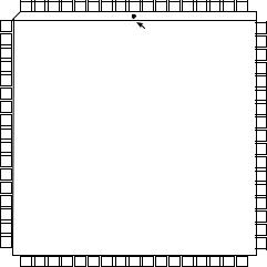
PIN CONFIGURATION
68-Lead Ceramic Leaded Chip Carrier
GNDA 10
GNDA 11
UPOSA 12
AVEE 13
AVCC 14
NC 15
NC 16
(LSB) D0A 17
D1A 18
D2A 19
D3A 20
D4A 21
D5A 22
D6A 23
D7A 24
D8A 25
GNDA 26
NC = NO CONNECT
GNDA |
A |
A |
A |
GNDA |
UCOMA |
UNEGA |
GNDA |
SHIELD |
GNDB |
AV |
AV |
GNDB |
A |
A |
A |
GNDB |
|
|
|
A3 |
A2 |
A1 |
|
|
|
|
|
|
EE |
CC |
|
B3 |
B2 |
B1 |
|
|
|
|
IN |
IN |
IN |
|
|
|
|
|
|
|
IN |
IN |
IN |
|
|
|
||
9 |
8 |
7 |
6 |
5 |
4 |
3 |
2 |
1 |
68 |
67 |
66 |
65 |
64 |
63 |
62 |
61 |
|
|
|
|
|
|
|
|
|
|
|
PIN 1 |
|
|
|
|
|
|
GNDB |
||
|
|
|
|
|
|
|
|
|
|
|
|
|
|
|
60 |
|||
|
|
|
|
|
|
|
|
|
IDENTIFIER |
|
|
|
|
|
GNDB |
|||
|
|
|
|
|
|
|
|
|
|
|
|
|
|
|||||
|
|
|
|
|
|
|
|
|
|
|
|
|
59 |
|||||
|
|
|
|
|
|
|
|
|
|
|
|
|
|
|
|
|
||
|
|
|
|
|
|
|
|
|
|
|
|
|
|
|
|
|
GNDB |
|
|
|
|
|
|
|
|
|
|
|
|
|
|
|
|
|
|
58 |
|
|
|
|
|
|
|
|
|
|
|
|
|
|
|
|
|
|
|
UPOSB |
|
|
|
|
|
|
|
|
|
|
|
|
|
|
|
|
|
57 |
|
|
|
|
|
|
|
|
|
|
|
|
|
|
|
|
|
|
UNEGB |
|
|
|
|
|
|
|
|
|
|
|
|
|
|
|
|
|
|
56 |
|
|
|
|
|
|
|
|
|
|
|
|
|
|
|
|
|
|
UCOMB |
|
|
|
|
|
|
|
|
|
|
|
|
|
|
|
|
|
|
55 |
|
|
|
|
|
|
|
|
|
|
|
|
|
|
|
|
|
|
GNDB |
|
|
|
|
|
|
|
|
|
|
|
|
|
|
|
|
|
|
54 |
|
|
|
|
|
|
|
|
AD10242 |
|
|
|
|
|
|
|
GNDB |
|||
|
|
|
|
|
|
|
|
|
|
|
|
|
|
53 |
||||
|
|
|
|
|
|
|
TOP VIEW |
|
|
|
|
|
|
|
|
ENCODEB |
||
|
|
|
|
|
|
|
|
|
|
|
|
|
|
52 |
||||
|
|
|
|
|
|
(Not to Scale) |
|
|
|
|
|
|
||||||
|
|
|
|
|
|
|
|
|
|
|
|
|
ENCODEB |
|||||
|
|
|
|
|
|
|
|
|
|
|
|
51 |
||||||
|
|
|
|
|
|
|
|
|
|
|
|
|
|
|
|
|
||
|
|
|
|
|
|
|
|
|
|
|
|
|
|
|
|
|
DVCC |
|
|
|
|
|
|
|
|
|
|
|
|
|
|
|
|
|
|
50 |
|
|
|
|
|
|
|
|
|
|
|
|
|
|
|
|
|
|
|
|
|
|
|
|
|
|
|
|
|
|
|
|
|
|
|
|
|
49 |
D11B (MSB) |
|
|
|
|
|
|
|
|
|
|
|
|
|
|
|
|
|
D10B |
|
|
|
|
|
|
|
|
|
|
|
|
|
|
|
|
|
|
48 |
|
|
|
|
|
|
|
|
|
|
|
|
|
|
|
|
|
|
D9B |
|
|
|
|
|
|
|
|
|
|
|
|
|
|
|
|
|
|
47 |
|
|
|
|
|
|
|
|
|
|
|
|
|
|
|
|
|
|
D8B |
|
|
|
|
|
|
|
|
|
|
|
|
|
|
|
|
|
|
46 |
|
|
|
|
|
|
|
|
|
|
|
|
|
|
|
|
|
|
D7B |
|
|
|
|
|
|
|
|
|
|
|
|
|
|
|
|
|
|
45 |
|
|
|
|
|
|
|
|
|
|
|
|
|
|
|
|
|
|
GNDB |
|
|
|
|
|
|
|
|
|
|
|
|
|
|
|
|
|
|
44 |
|
27 |
28 |
29 |
30 |
31 |
32 |
33 |
34 |
35 |
36 |
37 |
38 |
39 |
40 |
41 |
42 |
43 |
|
|
GNDA |
ENCODEA |
ENCODEA |
DV |
D9A |
D10A |
(MSB)D11A |
NC |
NC |
(LSB)D0B |
D1B |
D2B |
D3B |
D4B |
D5B |
D6B |
GNDB |
|
|
|
|
|
CC |
|
|
|
|
|
|
|
|
|
|
|
|
|
|
|
REV. B |
–5– |
Loading...