


BCP53
Siemens BCP53, BCP52-16, BCP52-10, BCP52, BCP51-16 Datasheet
...
Semiconductor Group 1
PNP Silicon AF Transistors BCP 51
... BCP 53
Type Marking
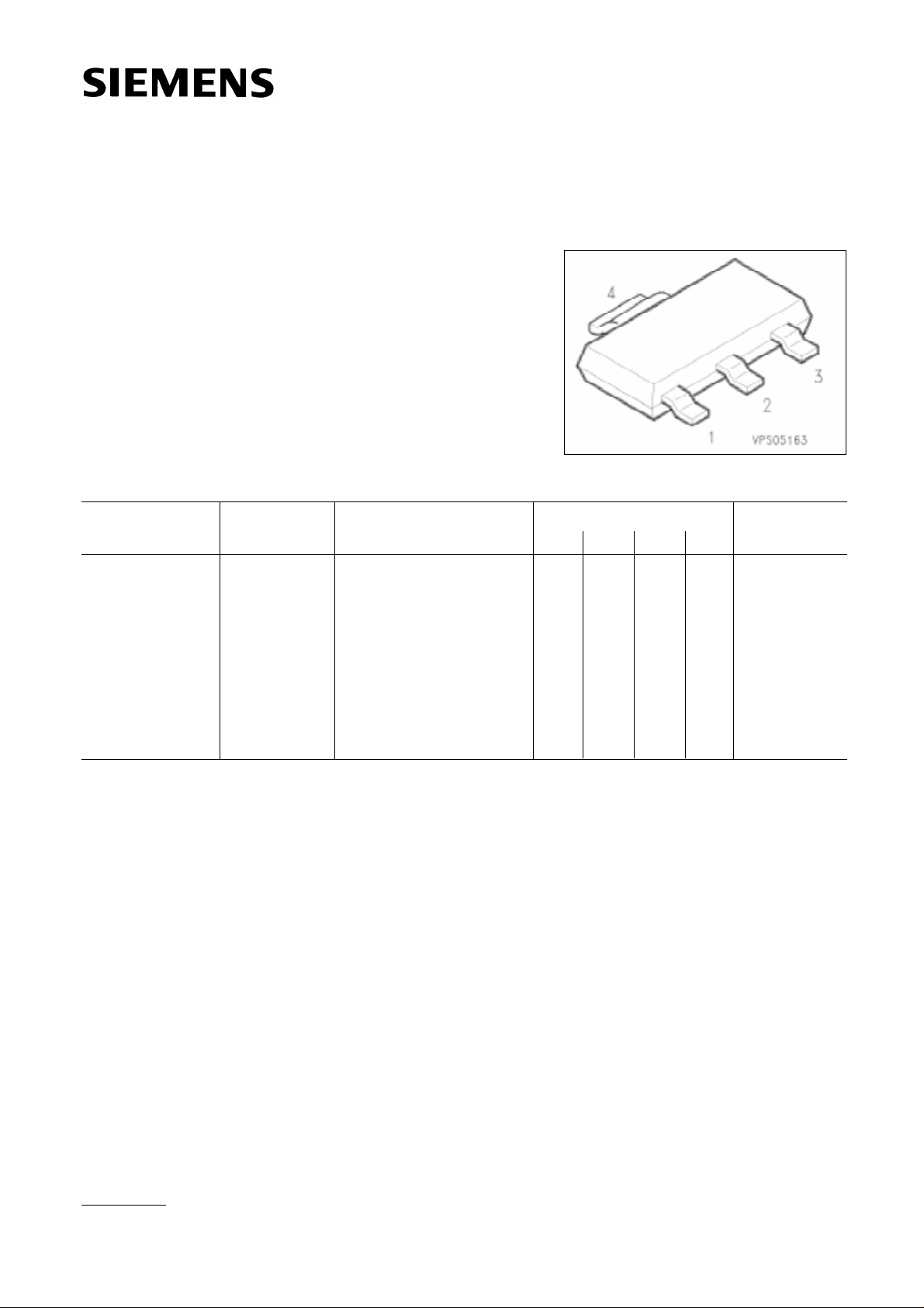
Package
1)
Pin Configuration
BCP 51
BCP 51-10
BCP 51-16
BCP 52
BCP 52-10
BCP 52-16
BCP 53
BCP 53-10
BCP 53-16
Q62702-C2107
Q62702-C2109
Q62702-C2110
Q62702-C2146
Q62702-C2112
Q62702-C2113
Q62702-C2147
Q62702-C2115
Q62702-C2116
BCP 51
BCP 51-10
BCP 51-16
BCP 52
BCP 52-10
BCP 52-16
BCP 53
BCP 53-10
BCP 53-16
SOT-223
1 2 3
Ordering Code
(tape and reel)
4
B C E C
1)
For detailed information see chapter Package Outlines.
● For AF driver and output stages
● High collector current
● Low collector-emitter saturation voltage
● Complementary types: BCP 54 … BCP 56 (NPN)
5.91
Semiconductor Group 2
BCP 51
... BCP 53
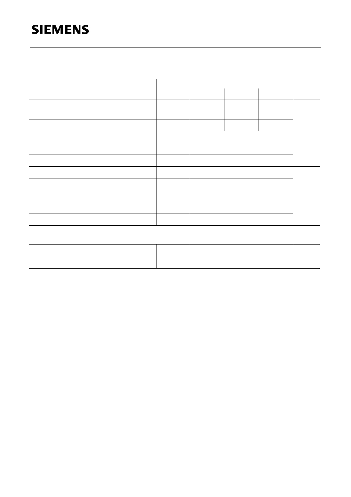
Maximum Ratings
Parameter Symbol
BCP 51 Unit
Collector-emitter voltage
R
BE ≤1kΩ
VCE0
VCER
45
45
V
Collector-base voltage VCB0 45
Emitter-base voltage V
EB0
Collector current IC A
Base current I
B mA
Total power dissipation, T
S =124 ˚C
1)
Ptot W
Junction temperature T
j ˚C
Storage temperature range T
stg – 65 … + 150
Thermal Resistance
Junction - ambient
1)
Rth JA ≤ 72 K/W
Peak collector current I
CM
Peak base current IBM
BCP 52
60
60
60
1
100
1.5
150
1.5
200
Values
BCP 53
80
100
100
5
Junction - soldering point Rth JS ≤ 17
1)
Package mounted on epoxy pcb 40 mm × 40 mm × 1.5 mm/6 cm
2
Cu.
 Loading...