


1N4933
1N4933, 1N4934, 1N4935,
f
1N4936, 1N4937
1N4935 and 1N4937 are Preferred Devices
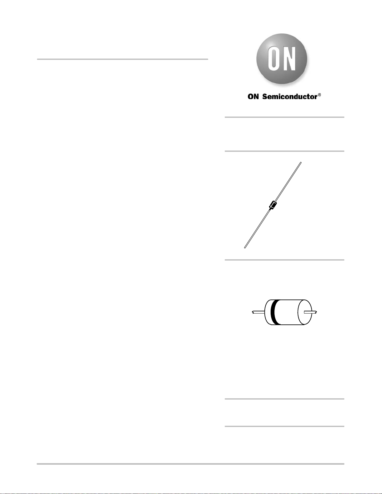
Axial−Lead Fast−Recovery
Rectifiers
Axial−lead, fast−recovery rectifiers are designed for special
applications such as DC power supplies, inverters, converters,
ultrasonic systems, choppers, low RF interference and free wheeling
diodes. A complete line of fast recovery rectifiers having typical
recovery time of 150 nanoseconds providing high efficiency at
frequencies to 250 kHz.
Features
• Shipped in Plastic Bags; 1,000 per Bag
• Available Tape and Reeled; 5,000 per Reel, by Adding a “RL” Suffix
to the Part Number
• These are Pb−Free Devices*
Mechanical Characteristics:
• Case: Epoxy, Molded
• Weight: 0.4 Gram (Approximately)
• Finish: All External Surfaces Corrosion Resistant and Terminal
Leads are Readily Solderable
• Lead Temperature for Soldering Purposes:
260°C Max. for 10 Seconds
• Polarity: Cathode Indicated by Polarity Band
http://onsemi.com
FAST RECOVERY RECTIFIERS
1.0 AMPERE, 50−600 VOLTS
AXIAL LEAD
CASE 59
STYLE 1
MARKING DIAGRAM
*For additional information on our Pb−Free strategy and soldering details, please
download the ON Semiconductor Soldering and Mounting Techniques
Reference Manual, SOLDERRM/D.
© Semiconductor Components Industries, LLC, 2006
July, 2006 − Rev. 12
1 Publication Order Number:
A
1N493x
YYWWG
G
A =Assembly Location
1N493x =Device Number
x= 3, 4, 5, 6 or 7
YY =Year
WW =Work Week
G =Pb−Free Package
(Note: Microdot may be in either location)
ORDERING INFORMATION
See detailed ordering and shipping information on page 3 o
this data sheet.
Preferred devices are recommended choices for future use
and best overall value.
1N4933/D
1N4933, 1N4934, 1N4935, 1N4936, 1N4937
MAXIMUM RATINGS (Note 1)
Rating Symbol 1N4933 1N4934 1N4935 1N4936 1N4937 Unit
†Peak Repetitive Reverse Voltage
Working Peak Reverse Voltage
DC Blocking Voltage
†Non−Repetitive Peak Reverse Voltage
RMS Reverse Voltage
†Average Rectified Forward Current
(Single phase, resistive load, TA = 75°C) (Note 2)
†Non−Repetitive Peak Surge Current
(Surge applied at rated load conditions)
Operating Junction Temperature Range
Storage Temperature Range
Stresses exceeding Maximum Ratings may damage the device. Maximum Ratings are stress ratings only. Functional operation above the
Recommended Operating Conditions is not implied. Extended exposure to stresses above the Recommended Operating Conditions may affect
device reliability.
1. Ratings at 25°C ambient temperature unless otherwise specified.
2. Derate by 20% for capacitive loads.
THERMAL CHARACTERISTICS
Characteristic Symbol Max Unit
Thermal Resistance, Junction−to−Ambient (Typical Printed Circuit Board Mounting)
ELECTRICAL CHARACTERISTICS
Characteristic Symbol Min Typ Max Unit
Instantaneous Forward Voltage (IF = 3.14 Amp, TJ = 150°C) v
Forward Voltage (IF = 1.0 Amp, TA = 25°C) V
†Reverse Current (Rated DC Voltage) TA = 25°C
REVERSE RECOVERY CHARACTERISTICS†
Reverse Recovery Time (IF = 1.0 Amp to VR = 30 Vdc)
(IFM = 15 Amp, di/dt = 10 A/ms)
Reverse Recovery Current (IF = 1.0 Amp to VR = 30 Vdc) I
†Indicates JEDEC Registered Data for 1N4933 Series.
V
RRM
V
RWM
V
V
RSM
V
R(RMS)
I
FSM
T
J,
50 100 200 400 600 V
R
75
35
I
O
150
70
250
140
450
280
650
420
1.0 A
V
30 A
T
stg
TA = 100°C
− 65 to +150 °C
R
q
JA
F
F
I
R
t
rr
RM(REC)
65 °C/W
− 1.0 1.2 V
− 1.05 1.2 V
−
1.0505.0
−
−
−
150
175
100
200
300
− 1.0 2.0 A
mA
ns
10
1
TC = 125°C
TC = 100°C
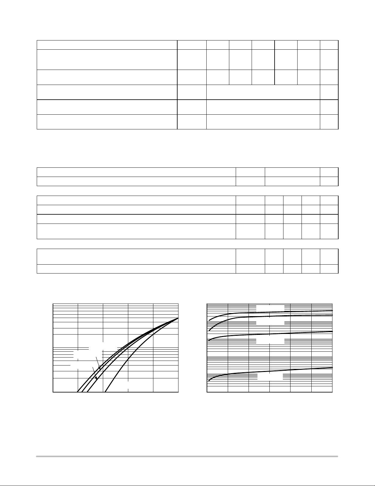
, FORWARD CURRENT (A)
F
I
0.1
VF, INSTANTANEOUS FORWARD VOLTAGE (V)
Figure 1. Typical Forward Voltage Figure 2. Typical Reverse Current
TC = 150°C
TC = 25°C
0.8 1.4
10.4 0.6
1.2
1.0E−03
1.0E−04
1.0E−05
1.0E−06
1.0E−07
, REVERSE CURRENT (A)
R
I
1.0E−08
http://onsemi.com
2
TC = 150°C
TC = 125°C
TC = 100°C
TC = 25°C
0 100 200 300 400 500
VR, REVERSE VOLTAGE (V)
600
 Loading...