


MSM51V8222A-40GS-K
OKI MSM51V8222A-40GS-K, MSM51V8222A-40JS, MSM51V8222A-40ZS, MSM51V8222A-30GS-K, MSM51V8222A-30JS Datasheet
...
E2L0055-28-Z2
¡ Semiconductor MSM51V8222A
¡ Semiconductor
This version: Dec. 1998
Previous version: Mar. 1998
MSM51V8222A
262,214-Word ¥ 8-Bit Field Memory
DESCRIPTION
The OKI MSM51V8222A is a high performance 2-Mbit, 256K ¥ 8-bit, Field Memory. It is designed
for high-speed serial access applications such as HDTVs, conventional NTSC TVs, VTRs, digital
movies and Multi-media systems. It is a FRAM for wide or low end use as general commodity
TVs and VTRs, exclusively. The MSM51V8222A is not designed for the other use or high end
use in medical systems, professional graphics systems which require long term picture, and
data storage systems and others. The 2-Mbit capacity fits one field of a conventional NTSC TV
screen. Two cascaded MSM51V8222As make one frame of the screen: two or more MSM51V8222As
can be cascaded directly without any delay devices between them. (Cascading provides larger
storage depth or a longer delay).
Each of the 8-bit planes has separate serial write and read ports. These employ independent control
clocks to support asynchronous read and write operations. Different clock rates are also supported,
which allow alternate data rates between write and read data streams.
The MSM51V8222A provides high speed FIFO, First-In First-Out, operation without external
refreshing: it refreshes its DRAM storage cells automatically, so that it appears fully static to the users.
Moreover, fully static type memory cells and decoders for serial access enable the refresh free serial
access operation, so that serial read and/or write control clock can be halted high or low for any
duration as long as the power is on. Internal conflicts of memory access and refreshing operations
are prevented by special arbitration logic.
The MSM51V8222A's function is simple, and similar to a digital delay device whose delay-bit-length
is easily set by reset timing. The delay length, and the number of read delay clocks between write
and read, is determined by externally controlled write and read reset timings.
Additional SRAM serial registers, or line buffers for the initial access of 256 ¥ 8-bit enable high speed
first-bit-access with no clock delay just after the write or read reset timings.
The MSM51V8222A is similar in operation and functionality to OKI 1-Mbit Field Memory
MSM51V4221C, with the addition of cascade capability. (As for MSM51V4221C operation
compatible 2-Mbit Field Memory, OKI has the MSM51V8221A which is a sister device of
MSM51V8222A).
Additionally, the MSM51V8222A has a write mask function or input enable function (IE), and readdata skipping function or output enable function (OE). The differences between write enable (WE)
and input enable (IE), and between read enable (RE) and output enable (OE) are that WE and RE can
stop serial write/read address increments, but IE and OE cannot stop the increment, when write/
read clocking is continuously applied to MSM51V8222A. The input enable (IE) function allows the
user to write into selected locations of the memory only, leaving the rest of the memory contents
unchanged. This facilitates data processing to display a "picture in picture" on a TV screen.
1/16
¡ Semiconductor MSM51V8222A
FEATURES
• Single power supply : 3.3 V ±0.3 V
• 512 Rows ¥ 512 Columns ¥ 8 bits
• Fast FIFO (First-In First-Out) operation
• High speed asynchronous serial access
Read/write cycle time 30 ns/40 ns
Access time 30 ns/35 ns
• Direct cascading capability
• Write mask function (Input enable control)
• Data skipping function (Output enable control)
• Self refresh (No refresh control is required)
• Package options :
28-pin 400 mil plastic ZIP (ZIP28-P-400-1.27) (Product : MSM51V8222A-xxZS)
28-pin 400 mil plastic SOJ (SOJ28-P-400-1.27) (Product : MSM51V8222A-xxJS)
28-pin 430 mil plastic SOP (SOP28-P-430-1.27-K) (Product : MSM51V8222A-xxGS-K)
xx indicates speed rank.
PRODUCT FAMILY
Family Access Time (Max.) Cycle Time (Min.) Package
MSM51V8222A-30ZS 30 ns30 ns
MSM51V8222A-40ZS 40 ns35 ns
MSM51V8222A-30JS
MSM51V8222A-40JS 40 ns35 ns
MSM51V8222A-30GS-K
MSM51V8222A-40GS-K
400 mil 28-pin ZIP
30 ns30 ns
30 ns30 ns
40 ns35 ns
400 mil 28-pin SOJ
430 mil 28-pin SOP
2/16
¡ Semiconductor MSM51V8222A
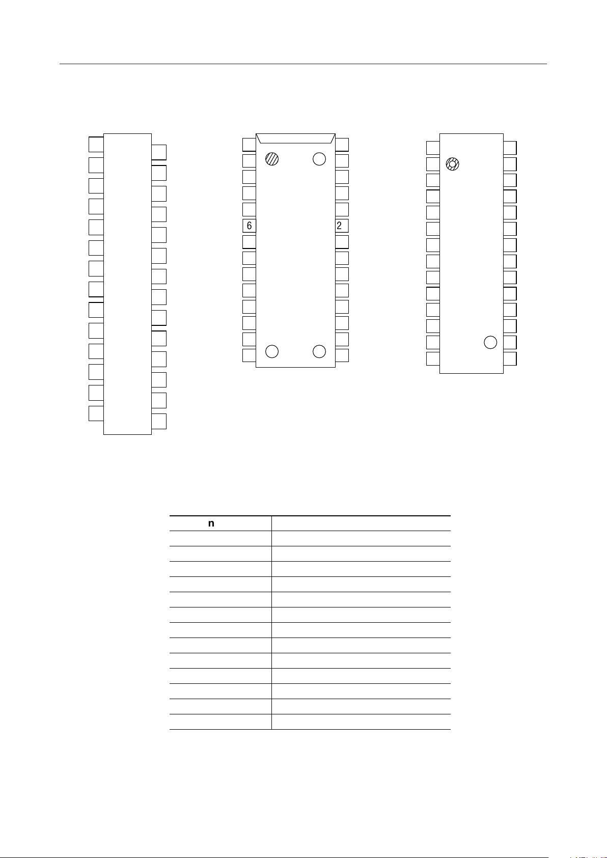
PIN CONFIGURATION (TOP VIEW)
WE
D
IN
DIN2
V
CC
DIN5
D
IN
SWCK
NC
OE
D
OUT
D
OUT
D
OUT
D
OUT
RSTR
1
3
0
5
7
9
7
11
13
15
17
19
6
21
4
23
3
25
1
27
10
12
14
16
18
20
22
24
26
28
2
4
6
8
IE
DIN1
DIN3
4
D
IN
6
D
IN
RSTW
NC
RE
D
OUT
D
OUT
V
SS
D
OUT
D
OUT
SRCK
DIN4
1
D
5
2
IN
6
D
3
IN
D
7
4
IN
RSTW
SWCK
D
D
7
D
5
D
5
623
722
NC
RE
821
OE
9
10
7
OUT
11
6
OUT
12
5
OUT
13
4
OUT
14 15
V
SS
28
27
26
25
24
20
19
18
17
16
V
CC
DIN3
2
D
IN
D
1
IN
0
D
IN
IE
WE
NC
SRCK
RSTR
D
OUT
D
OUT
D
OUT
D
OUT
1
4
D
IN
5
D
2
IN
D
3
6
IN
7
4
D
IN
RSTW
SWCK
5
6
NC
RE
8
OE
9
D
10
7
OUT
0
1
2
3
11
D
6
OUT
12
D
5
OUT
13
4
D
OUT
V
14 15
SS
28
27
26
25
24
23
227
21
20
19
18
17
16
V
CC
DIN3
D
2
IN
1
D
IN
D
0
IN
IE
WE
NC
SRCK
RSTR
D
OUT
D
OUT
D
OUT
D
OUT
2
0
28-Pin Plastic SOJ
28-Pin Plastic SOP
0
1
2
3
28-Pin Plastic ZIP
Pin Name Function
SWCK
SRCK
RSTW
RSTR
D
IN
D
OUT
WE
RE
IE
OE
0 - 7
V
CC
V
SS
0 - 7
Serial Write Clock
Serial Read Clock
Write Enable
Read Enable
Input Enable
Output Enable
Write Reset Clock
Read Reset Clock
Data Input
Data Output
Power Supply (3.3 V)
Ground (0 V)
NC No Connection
3/16
4/16
¡ Semiconductor MSM51V8222A
BLOCK DIAGRAM
D
OUT
(¥ 8)
Data-out
Buffer (¥ 8)
OE
RE
RSTR SRCK
Serial
512-Word Serial Read Register (¥ 8)
Read Line Buffer
Low-Half (¥ 8)
Read Line Buffer
High-Half (¥ 8)
256 (¥ 8)
256K (¥ 8)
Memory
Array
X
Decoder
71-Word
Sub-Register (¥ 8)
Read/Write
and Refresh
Controller
Clock
Oscillator
Write Line Buffer
Low-Half (¥ 8)
Write Line Buffer
High-Half (¥ 8)
512-Word Serial Write Register (¥ 8)
Data-in
Buffer (¥ 8)
D
IN
(¥ 8)
Serial
IE WE RSTW SWCK
71-Word
Sub-Register (¥ 8)
256 (¥ 8)
256 (¥ 8)
256 (¥ 8)
V
BB
Generator
Read
Controller
Write
Controller

¡ Semiconductor MSM51V8222A
OPERATION
Write Operation
The write operation is controlled by three clocks, SWCK, RSTW, and WE. Write operation is
accomplished by cycling SWCK, and holding WE high after the write address pointer reset operation
or RSTW.
Each write operation, which begins after RSTW, must contain at least 80 active write cycles, i.e.
SWCK cycles while WE is high. To transfer the last data to the DRAM array, which at that time
is stored in the serial data registers attached to the DRAM array, an RSTW operation is required
after the last SWCK cycle.
Note that every write timing of MSM51V8222A is delayed by one clock compared with read timings
for easy cascading without any interface delay devices.
Write Reset : RSTW
The first positive transition of SWCK after RSTW becomes high resets the write address counters to
zero. RSTW setup and hold times are referenced to the rising edge of SWCK. Because the write reset
function is solely controlled by the SWCK rising edge after the high level of RSTW, the states of WE
and IE are ignored in the write reset cycle.
Before RSTW may be brought high again for a further reset operation, it must be low for at least two
SWCK cycles.
Data Inputs : DIN0 - 7
Write Clock : SWCK
The SWCK latches the input data on chip when WE is high, and also increments the internal write
address pointer. Data-in setup time tDS, and hold time tDH are referenced to the rising edge of SWCK.
Write Enable : WE
WE is used for data write enable/disable control. WE high level enables the input, and WE low level
disables the input and holds the internal write address pointer. There are no WE disable time (low)
and WE enable time (high) restrictions, because the MSM51V8222A is in fully static operation as long
as the power is on. Note that WE setup and hold times are referenced to the rising edge of SWCK.
Input Enable : IE
IE is used to enable/disable writing into memory. IE high level enables writing. The internal write
address pointer is always incremented by cycling SWCK regardless of the IE level. Note that IE setup
and hold times are referenced to the rising edge of SWCK.
5/16

¡ Semiconductor MSM51V8222A
Read Operation
The read operation is controlled by three clocks, SRCK, RSTR, and RE. Read operation is
accomplished by cycling SRCK, and holding RE high after the read address pointer reset operation
or RSTR.
Each read operation, which begins after RSTR, must contain at least 80 active read cycles, i.e. SRCK
cycles while RE is high.
Read Reset : RSTR
The first positive transition of SRCK after RSTR becomes high resets the read address counters to
zero. RSTR setup and hold times are referenced to the rising edge of SRCK. Because the read reset
function is solely controlled by the SRCK rising edge after the high level of RSTR, the states of RE and
OE are ignored in the read reset cycle.
Before RSTR may be brought high again for a further reset operation, it must be low for at least *two
SRCK cycles.
Data Out : D
OUT
0 - 7
Read Clock : SRCK
Data is shifted out of the data registers. It is triggered by the rising edge of SRCK when RE is high
during a read operation. The SRCK input increments the internal read address pointer when RE is
high.
The three-state output buffer provides direct TTL compatibility (no pullup resistor required). Data
out is the same polarity as data in. The output becomes valid after the access time interval tAC that
begins with the rising edge of SRCK. *There are no output valid time restrictions on MSM51V8222A.
Read Enable : RE
The function of RE is to gate the SRCK clock for incrementing the read pointer. When RE is high
before the rising edge of SRCK, the read pointer is incremented. When RE is low, the read pointer
is not incremented. RE setup times (t
RENS
and t
) and RE hold times (t
RDSS
RENH
and t
RDSH
) are
referenced to the rising edge of the SRCK clock.
Output Enable : OE
OE is used to enable/disable the outputs. OE high level enables the outputs. The internal read
address pointer is always incremented by cycling SRCK regardless of the OE level. Note that OE
setup and hold times are referenced to the rising edge of SRCK.
6/16
 Loading...