


OKI MSM518122-80JS, MSM518122-70JS, MSM518122-80ZS, MSM518122-70ZS, MSM518122-10JS Datasheet
...E2L0015-17-Y1
This version: Jan. 1998
¡SemiconductorSemiconductor MSM518122
Previous version: Dec. 1996
MSM518122
131,072-Word ´ 8-Bit Multiport DRAM
DESCRIPTION
The MSM518122 is an 1-Mbit CMOS multiport DRAM composed of a 131,072-word by 8-bit dynamic RAM and a 256-word by 8-bit SAM. Its RAM and SAM operate independently and asynchronously.
The MSM518122 supports three types of operation : random access to RAM port, high speed serial access to SAM port and bidirectional transfer of data between any selected row in the RAM port and the SAM port. In addition to the conventional multiport DRAM operating modes, the MSM518122 features the block write and flash write functions on the RAM port and a split data transfer capability on the SAM port. The SAM port requires no refresh operation because it uses static CMOS flip-flops.
FEATURES
•Single power supply: 5 V ±10%
•Full TTL compatibility
•Multiport organization
RAM: 128K word ´ 8 bits
SAM: 256 word ´ 8 bits
•Fast page mode
•Write per bit
•Masked flash write
•Masked block write
•RAS only refresh
•CAS before RAS refresh
•Hidden refresh
•Serial read/write
•256 tap location
•Bidirectional data transfer
•Split transfer
•Masked write transfer
•Refresh: 512 cycles/8 ms
•Package options:
40-pin 475 mil plastic ZIP |
(ZIP40-P-475-1.27) |
(Product : MSM518122-xxZS) |
40-pin 400 mil plastic SOJ |
(SOJ40-P-400-1.27) |
(Product : MSM518122-xxJS) |
|
|
xx indicates speed rank. |
PRODUCT FAMILY
Family |
Access Time |
Cycle Time |
Power Dissipation |
||||
|
|
|
|
|
|
||
RAM |
SAM |
RAM |
SAM |
Operating |
Standby |
||
|
|||||||
|
|
|
|
|
|
|
|
MSM518122-70 |
70 ns |
25 ns |
140 ns |
30 ns |
120 mA |
8 mA |
|
|
|
|
|
|
|
|
|
MSM518122-80 |
80 ns |
25 ns |
150 ns |
30 ns |
110 mA |
8 mA |
|
|
|
|
|
|
|
|
|
MSM518122-10 |
100 ns |
25 ns |
180 ns |
30 ns |
100 mA |
8 mA |
|
|
|
|
|
|
|
|
|
1/45

¡ Semiconductor |
MSM518122 |
PIN CONFIGURATION (TOP VIEW)
|
|
|
|
|
W5/IO5 |
1 |
|
|
|
|
2 |
W6/IO6 |
||
|
|
|
||
W7/IO7 |
3 |
|
||
|
|
|
||
|
4 |
W8/IO8 |
||
SE |
|
|
||
5 |
|
|||
|
|
|
||
|
6 |
SIO5 |
||
|
|
|
||
SIO6 |
7 |
|
||
|
|
|
||
|
8 |
SIO7 |
||
|
|
|
||
SIO8 |
9 |
|
||
|
|
|
||
|
10 |
VSS1 |
||
|
|
|
||
SC |
11 |
|
||
|
|
|
||
|
12 |
SIO1 |
||
|
|
|
||
SIO2 |
13 |
|
||
|
|
|
||
|
14 |
SIO3 |
||
|
|
|
||
SIO4 |
15 |
|
||
|
|
DT/OE |
||
|
16 |
|||
|
|
|
||
W1/IO1 |
17 |
|
||
|
|
|
||
|
18 |
W2/IO2 |
||
|
|
|
||
W3/IO3 |
19 |
|
||
|
|
|
||
|
20 |
NC |
||
|
|
|
||
W4/IO4 |
21 |
|
||
|
|
|
||
|
22 |
VCC1 |
||
WB/WE |
|
|
||
23 |
|
|||
|
|
RAS |
||
|
24 |
|||
|
|
|
||
A8 |
25 |
|
||
|
|
|
||
|
26 |
A6 |
||
|
|
|
||
VSS2 |
27 |
|
||
|
|
|
||
|
28 |
NC |
||
|
|
|
||
A5 |
29 |
|
||
|
|
|
||
|
30 |
A4 |
||
|
|
|
||
NC |
31 |
|
||
|
|
|
||
|
32 |
VCC2 |
||
|
|
|
||
A7 |
33 |
|
||
|
|
|
||
|
34 |
A3 |
||
|
|
|
||
A2 |
35 |
|
||
|
|
|
||
|
36 |
A1 |
||
|
|
|
||
A0 |
37 |
|
||
|
|
|
||
|
38 |
QSF |
||
CAS |
|
|
||
39 |
|
|||
|
|
|
||
|
40 |
DSF |
||
|
|
|
||
|
|
|
|
|
40-Pin Plastic ZIP
|
|
|
|
|
SC |
1 |
|
40 |
VSS1 |
|
|
|
|
|
SIO1 |
2 |
|
39 |
SIO8 |
|
|
|
|
|
SIO2 |
3 |
|
38 |
SIO7 |
|
|
|
|
|
SIO3 |
4 |
|
37 |
SIO6 |
|
|
|
|
|
SIO4 |
5 |
|
36 |
SIO5 |
DT/OE |
|
|
|
SE |
6 |
|
35 |
||
|
|
|
|
|
W1/IO1 |
7 |
|
34 |
W8/IO8 |
|
|
|
|
|
W2/IO2 |
8 |
|
33 |
W7/IO7 |
|
|
|
|
|
W3/IO3 |
9 |
|
32 |
W6/IO6 |
|
|
|
|
|
W4/IO4 |
10 |
|
31 |
W5/IO5 |
|
|
|
|
|
VCC1 |
11 |
|
30 |
VSS2 |
|
|
|
|
|
WB/WE |
12 |
|
29 |
DSF |
|
|
|
|
|
NC |
13 |
|
28 |
NC |
RAS |
|
|
|
CAS |
14 |
|
27 |
||
|
|
|
|
|
NC |
15 |
|
26 |
QSF |
|
|
|
|
|
A8 |
16 |
|
25 |
A0 |
|
|
|
|
|
A6 |
17 |
|
24 |
A1 |
|
|
|
|
|
A5 |
18 |
|
23 |
A2 |
|
|
|
|
|
A4 |
19 |
|
22 |
A3 |
|
|
|
|
|
VCC2 |
20 |
|
21 |
A7 |
|
|
|
|
|
40-Pin Plastic SOJ
Pin Name |
Function |
Pin Name |
Function |
|
|
|
|
A0 - A8 |
Address Input |
SC |
Serial Clock |
W1/IO1 - W8/IO8 |
RAM Inputs/Outputs |
SE |
SAM Port Enable |
SIO1 - SIO8 |
SAM Inputs/Outputs |
DSF |
Special Function Input |
RAS |
Row Address Strobe |
QSF |
Special Function Output |
CAS |
Column Address Strobe |
VCC |
Power Supply (5 V) |
WB/WE |
Write per Bit/Write Enable |
VSS |
Ground (0 V) |
DT/OE |
Transfer/Output Enable |
NC |
No Connection |
Note : The same power supply voltage must be provided to every VCC pin, and the same GND voltage level must be provided to every VSS pin.
2/45
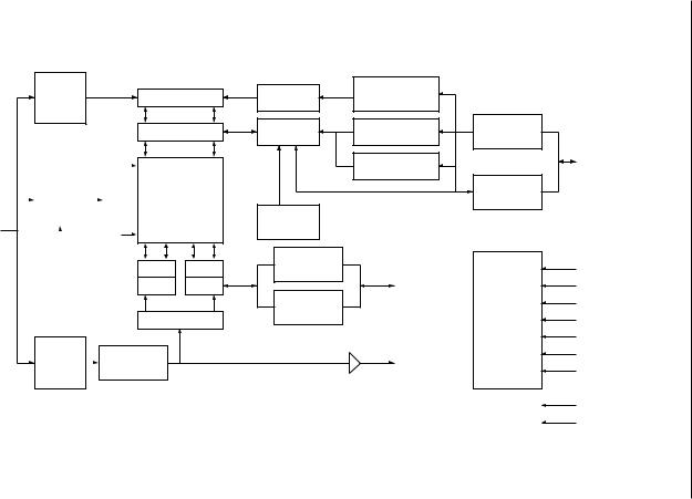
A0 - A8
3/45
Column
Address
Buffer
|
|
|
|
Row |
|
Row |
|||
|
|
Decoder |
||
|
Address |
|
||
|
|
|
||
|
Buffer |
|
|
|
|
|
|
|
|
|
|
|
|
|
|
|
|
|
|
|
Refresh |
|
|
|
|
Counter |
|
|
|
Column Decoder
Sense Amp.
512 ´ 256 ´ 8 RAM ARRAY
Gate Gate
SAM SAM
Serial Decoder
SAM
Address
SAM Address
Buffer
Counter
Block Write |
Column Mask |
|
|
Register |
|
||
Control |
|
||
|
|
||
I/O Control |
Color Register |
RAM Input |
|
Buffer |
|||
|
|
||
|
Mask Register |
|
|
|
|
RAM Output |
|
|
|
Buffer |
|
Flash Write |
|
|
|
Control |
|
|
|
SAM Input |
|
|
|
Buffer |
SIO1 |
|
|
|
|
||
SAM Output |
- SIO8 |
|
|
|
Timing |
||
Buffer |
|
||
|
Generator |
||
|
|
||
|
QSF |
|
W1/IO1
- W8/IO8
RAS
CAS
DT/OE WB/WE
DSF
SC
SE
VCC
VSS
DIAGRAM BLOCK |
Semiconductor ¡ |
MSM518122
¡ Semiconductor |
MSM518122 |
ELECTRICAL CHARACTERISTICS |
|
|
|
|
|
|
|
|
|
|||||
Absolute Maximum Ratings |
|
|
|
|
|
|
|
|
|
(Note: 16) |
||||
|
|
|
|
|
|
|
|
|
|
|
|
|
|
|
|
|
|
|
|
|
|
|
|
|
|
|
|
|
|
|
|
Parameter |
|
|
Symbol |
Condition |
|
|
|
Rating |
Unit |
|||
|
|
|
|
|
|
|
|
|
|
|
|
|
||
|
Input Output Voltage |
|
|
VT |
Ta = 25°C |
|
|
–1.0 to 7.0 |
V |
|||||
|
Output Current |
|
|
IOS |
Ta = 25°C |
|
|
|
50 |
mA |
||||
|
Power Dissipation |
|
|
PD |
Ta = 25°C |
|
|
|
1 |
W |
||||
|
Operating Temperature |
|
|
Topr |
— |
|
|
|
0 to 70 |
°C |
||||
|
Storage Temperature |
|
|
Tstg |
— |
|
|
–55 to 150 |
°C |
|||||
|
Recommended Operating Condition |
|
|
|
|
|
(Ta = 0°C to 70°C) (Note: 17) |
|||||||
|
|
|
|
|
|
|
|
|
|
|
||||
|
|
|
|
|
|
|
|
|
|
|
|
|
|
|
|
|
Parameter |
|
|
Symbol |
Min. |
|
Typ. |
|
|
Max. |
Unit |
||
|
|
|
|
|
|
|
|
|
|
|
|
|
|
|
|
Power Supply Voltage |
|
|
VCC |
4.5 |
|
5.0 |
|
5.5 |
V |
||||
|
Input High Voltage |
|
|
VIH |
2.4 |
|
|
— |
|
6.5 |
V |
|||
|
Input Low Voltage |
|
|
VIL |
–1.0 |
|
|
— |
|
0.8 |
V |
|||
Capacitance |
|
|
|
|
(VCC = 5 V ±10%, f = 1 MHz, Ta = 25°C) |
|||||||||
|
|
|
|
|
|
|
|
|
||||||
|
|
Parameter |
|
Symbol |
Min. |
|
|
|
|
Max. |
Unit |
|||
|
|
|
|
|
|
|
|
|
|
|
|
|||
|
Input Capacitance |
|
CI |
— |
|
|
|
7 |
pF |
|||||
|
Input/Output Capacitance |
|
CI/O |
— |
|
|
|
9 |
pF |
|||||
|
Output Capacitance |
|
CO(QSF) |
— |
|
|
|
9 |
pF |
|||||
Note: |
This parameter is periodically sampled and is not 100% tested. |
|
||||||||||||
DC Characteristics 1 |
|
|
|
|
|
|
|
|
|
|
||||
|
|
|
|
|
|
|
|
|
|
|
|
|
||
|
|
Parameter |
|
Symbol |
Condition |
|
|
Min. |
|
|
Max. |
Unit |
||
|
|
|
|
|
|
|
|
|
|
|
||||
|
Output "H" Level Voltage |
|
VOH |
IOH = –2 mA |
|
2.4 |
|
|
— |
V |
||||
|
Output "L" Level Voltage |
|
|
VOL |
IOL = 2 mA |
|
|
— |
|
|
0.4 |
|||
|
|
|
|
|
|
|||||||||
|
|
|
|
|
|
0 £ VIN £ VCC |
|
|
|
|
|
|
|
|
|
Input Leakage Current |
|
ILI |
All other pins not |
|
|
–10 |
|
10 |
|
||||
|
|
|
|
|
|
under test = 0 V |
|
|
|
|
|
|
mA |
|
|
Output Leakage Current |
|
|
ILO |
0 £ VOUT £ 5.5 V |
|
|
–10 |
|
|
10 |
|
||
|
|
Output Disable |
|
|
|
|
||||||||
|
|
|
|
|
|
|
|
|
|
|
|
|
||
|
|
|
|
|
|
|
|
|
|
|
|
|
|
|
4/45
¡ Semiconductor |
|
|
|
|
MSM518122 |
|||
DC Characteristics 2 |
|
|
(VCC = 5 V ±10%, Ta = 0°C to 70°C) |
|||||
|
|
|
||||||
Item (RAM) |
SAM |
Symbol |
-70 |
-80 |
-10 |
Unit |
Note |
|
|
|
|
||||||
Max. |
Max. |
Max. |
||||||
|
|
|
|
|
||||
|
|
|
|
|
|
|
|
|
Operating Current |
Standby |
ICC1 |
85 |
75 |
65 |
|
1, 2 |
|
(RAS, CAS Cycling, tRC = tRC min.) |
Active |
ICC1A |
120 |
110 |
100 |
|
1, 2 |
|
Standby Current |
Standby |
ICC2 |
8 |
8 |
8 |
|
3 |
|
(RAS, CAS = VIH) |
Active |
ICC2A |
50 |
45 |
40 |
|
1, 2 |
|
RAS Only Refresh Current |
Standby |
ICC3 |
85 |
75 |
65 |
|
1, 2 |
|
(RAS Cycling, CAS = VIH, tRC = tRC min.) |
Active |
ICC3A |
120 |
110 |
100 |
|
1, 2 |
|
Page Mode Current |
Standby |
ICC4 |
70 |
65 |
60 |
|
1, 2 |
|
(RAS = VIL, CAS Cycling, tPC = tPC min.) |
Active |
ICC4A |
120 |
110 |
100 |
mA |
1, 2 |
|
CAS before RAS Refresh Current |
Standby |
ICC5 |
85 |
75 |
65 |
1, 2 |
||
|
||||||||
(RAS Cycling, CAS before RAS, tRC = tRC min.) |
Active |
ICC5A |
120 |
110 |
100 |
|
1, 2 |
|
Data Transfer Current |
Standby |
ICC6 |
85 |
75 |
65 |
|
1, 2 |
|
(RAS, CAS Cycling, tRC = tRC min.) |
Active |
ICC6A |
120 |
110 |
100 |
|
1, 2 |
|
Flash Write Current |
Standby |
ICC7 |
85 |
75 |
65 |
|
1, 2 |
|
(RAS, CAS Cycling, tRC = tRC min.) |
Active |
ICC7A |
120 |
110 |
100 |
|
1, 2 |
|
Block Write Current |
Standby |
ICC8 |
85 |
75 |
65 |
|
1, 2 |
|
(RAS, CAS Cycling, tRC = tRC min.) |
Active |
ICC8A |
120 |
110 |
100 |
|
1, 2 |
|
5/45
¡ Semiconductor |
|
|
|
|
|
|
MSM518122 |
|||
AC Characteristics (1/3) |
|
(VCC = 5 V ±10%, Ta = 0°C to 70°C) Note 4, 5, 6 |
||||||||
|
|
|||||||||
Parameter |
Symbol |
-70 |
-80 |
-10 |
Unit |
Note |
||||
Min. |
Max. |
Min. |
Max. |
Min. |
Max. |
|||||
|
|
|
|
|||||||
Random Read or Write Cycle Time |
tRC |
140 |
— |
150 |
— |
180 |
— |
ns |
|
|
Read Modify Write Cycle Time |
tRWC |
195 |
— |
195 |
— |
235 |
— |
ns |
|
|
Fast Page Mode Cycle Time |
tPC |
45 |
— |
50 |
— |
55 |
— |
ns |
|
|
Fast Page Mode Read Modify Write Cycle Time |
tPRWC |
90 |
— |
90 |
— |
100 |
— |
ns |
|
|
Access Time from RAS |
tRAC |
— |
70 |
— |
80 |
— |
100 |
ns |
7, 13 |
|
Access Time from Column Address |
tAA |
— |
35 |
— |
40 |
— |
55 |
ns |
7, 13 |
|
Access Time from CAS |
tCAC |
— |
20 |
— |
25 |
— |
25 |
ns |
7, 14 |
|
Access Time from CAS Precharge |
tCPA |
— |
40 |
— |
45 |
— |
50 |
ns |
7, 14 |
|
Output Buffer Turn-off Delay |
tOFF |
0 |
20 |
0 |
20 |
0 |
20 |
ns |
9 |
|
Transition Time (Rise and Fall) |
tT |
3 |
35 |
3 |
35 |
3 |
35 |
ns |
6 |
|
RAS Precharge Time |
tRP |
60 |
— |
60 |
— |
70 |
— |
ns |
|
|
RAS Pulse Width |
tRAS |
70 |
10k |
80 |
10k |
100 |
10k |
ns |
|
|
RAS Pulse Width (Fast Page Mode Only) |
tRASP |
70 |
100k |
80 |
100k |
100 |
100k |
ns |
|
|
RAS Hold Time |
tRSH |
20 |
— |
25 |
— |
25 |
— |
ns |
|
|
CAS Hold Time |
tCSH |
70 |
— |
80 |
— |
100 |
— |
ns |
|
|
CAS Pulse Width |
tCAS |
20 |
10k |
25 |
10k |
25 |
10k |
ns |
|
|
RAS to CAS Delay Time |
tRCD |
20 |
50 |
20 |
55 |
20 |
75 |
ns |
13 |
|
RAS to Column Address Delay Time |
tRAD |
15 |
35 |
15 |
40 |
20 |
50 |
ns |
13 |
|
Column Address to RAS Lead Time |
tRAL |
35 |
— |
40 |
— |
55 |
— |
ns |
|
|
CAS to RAS Precharge Time |
tCRP |
10 |
— |
10 |
— |
10 |
— |
ns |
|
|
CAS Precharge Time |
tCPN |
10 |
— |
10 |
— |
10 |
— |
ns |
|
|
CAS Precharge Time (Fast Page Mode) |
tCP |
10 |
— |
10 |
— |
10 |
— |
ns |
|
|
Row Address Set-up Time |
tASR |
0 |
— |
0 |
— |
0 |
— |
ns |
|
|
Row Address Hold Time |
tRAH |
10 |
— |
10 |
— |
10 |
— |
ns |
|
|
Column Address Set-up Time |
tASC |
0 |
— |
0 |
— |
0 |
— |
ns |
|
|
Column Address Hold Time |
tCAH |
15 |
— |
15 |
— |
15 |
— |
ns |
|
|
Column Address Hold Time referenced to RAS |
tAR |
55 |
— |
55 |
— |
70 |
— |
ns |
|
|
Read Command Set-up Time |
tRCS |
0 |
— |
0 |
— |
0 |
— |
ns |
|
|
Read Command Hold Time |
tRCH |
0 |
— |
0 |
— |
0 |
— |
ns |
10 |
|
Read Command Hold Time referenced to RAS |
tRRH |
0 |
— |
0 |
— |
0 |
— |
ns |
10 |
|
Write Command Hold Time |
tWCH |
15 |
— |
15 |
— |
15 |
— |
ns |
|
|
Write Command Hold Time referenced to RAS |
tWCR |
55 |
— |
55 |
— |
70 |
— |
ns |
|
|
Write Command Pulse Width |
tWP |
15 |
— |
15 |
— |
15 |
— |
ns |
|
|
Write Command to RAS Lead Time |
tRWL |
20 |
— |
20 |
— |
25 |
— |
ns |
|
|
Write Command to CAS Lead Time |
tCWL |
20 |
— |
20 |
— |
25 |
— |
ns |
|
|
6/45
¡ Semiconductor |
|
|
|
|
|
|
MSM518122 |
|
|||
AC Characteristics (2/3) |
|
(VCC = 5 V ±10%, Ta = 0°C to 70°C) Note 4, 5, 6 |
|
||||||||
|
|
|
|
||||||||
|
Parameter |
Symbol |
-70 |
-80 |
-10 |
Unit |
Note |
|
|||
|
Min. |
Max. |
Min. |
Max. |
Min. |
Max. |
|
||||
|
|
|
|
|
|
||||||
|
Data Set-up Time |
tDS |
0 |
— |
0 |
— |
0 |
— |
ns |
11 |
|
|
Data Hold Time |
tDH |
15 |
— |
15 |
— |
15 |
— |
ns |
11 |
|
|
Data Hold Time referenced to RAS |
tDHR |
55 |
— |
55 |
— |
70 |
— |
ns |
|
|
|
Write Command Set-up Time |
tWCS |
0 |
— |
0 |
— |
0 |
— |
ns |
12 |
|
|
RAS to WE Delay Time |
tRWD |
100 |
— |
100 |
— |
130 |
— |
ns |
12 |
|
|
Column Address to WE Delay Time |
tAWD |
65 |
— |
65 |
— |
80 |
— |
ns |
12 |
|
|
CAS to WE Delay Time |
tCWD |
45 |
— |
45 |
— |
55 |
— |
ns |
12 |
|
|
Data to CAS Delay Time |
tDZC |
0 |
— |
0 |
— |
0 |
— |
ns |
|
|
|
Data to OE Delay Time |
tDZO |
0 |
— |
0 |
— |
0 |
— |
ns |
|
|
|
Access Time from OE |
tOEA |
— |
20 |
— |
20 |
— |
25 |
ns |
7 |
|
|
Output Buffer Turn-off Delay from OE |
tOEZ |
0 |
10 |
0 |
10 |
0 |
20 |
ns |
9 |
|
|
OE to Data Delay Time |
tOED |
10 |
— |
10 |
— |
20 |
— |
ns |
|
|
|
OE Command Hold Time |
tOEH |
10 |
— |
10 |
— |
20 |
— |
ns |
|
|
|
RAS Hold Time referenced to OE |
tROH |
15 |
— |
15 |
— |
15 |
— |
ns |
|
|
|
CAS Set-up Time for CAS before RAS Cycle |
tCSR |
10 |
— |
10 |
— |
10 |
— |
ns |
|
|
|
CAS Hold Time for CAS before RAS Cycle |
tCHR |
10 |
— |
10 |
— |
10 |
— |
ns |
|
|
|
RAS Precharge to CAS Active Time |
tRPC |
0 |
— |
0 |
— |
0 |
— |
ns |
|
|
|
Refresh Period |
tREF |
— |
8 |
— |
8 |
— |
8 |
ms |
|
|
|
WB Set-up Time |
tWSR |
0 |
— |
0 |
— |
0 |
— |
ns |
|
|
|
WB Hold Time |
tRWH |
15 |
— |
15 |
— |
15 |
— |
ns |
|
|
|
DSF Set-up Time referenced to RAS |
tFSR |
0 |
— |
0 |
— |
0 |
— |
ns |
|
|
|
DSF Hold Time referenced to RAS (1) |
tRFH |
15 |
— |
15 |
— |
15 |
— |
ns |
|
|
|
DSF Hold Time referenced to RAS (2) |
tFHR |
55 |
— |
55 |
— |
70 |
— |
ns |
|
|
|
DSF Set-up Time referenced to CAS |
tFSC |
0 |
— |
0 |
— |
0 |
— |
ns |
|
|
|
DSF Hold Time referenced to CAS |
tCFH |
15 |
— |
15 |
— |
15 |
— |
ns |
|
|
|
Write Per Bit Mask Data Set-up Time |
tMS |
0 |
— |
0 |
— |
0 |
— |
ns |
|
|
|
Write Per Bit Mask Data Hold Time |
tMH |
15 |
— |
15 |
— |
15 |
— |
ns |
|
|
|
DT High Set-up Time |
tTHS |
0 |
— |
0 |
— |
0 |
— |
ns |
|
|
|
DT High Hold Time |
tTHH |
15 |
— |
15 |
— |
15 |
— |
ns |
|
|
|
DT Low Set-up Time |
tTLS |
0 |
— |
0 |
— |
0 |
— |
ns |
|
|
|
DT Low Hold Time |
tTLH |
15 |
10k |
15 |
10k |
15 |
10k |
ns |
|
|
|
DT Low Hold Time referenced to RAS |
tRTH |
60 |
10k |
65 |
10k |
80 |
10k |
ns |
|
|
|
(Real Time Read Transfer) |
|
|
||||||||
|
|
|
|
|
|
|
|
|
|
|
|
|
DT Low Hold Time referenced to Column Address |
tATH |
25 |
— |
30 |
— |
30 |
— |
ns |
|
|
|
(Real Time Read Transfer) |
|
|
||||||||
|
|
|
|
|
|
|
|
|
|
|
|
|
DT Low Hold Time referenced to CAS |
tCTH |
20 |
— |
25 |
— |
25 |
— |
ns |
|
|
|
(Real Time Read Transfer) |
|
|
||||||||
|
|
|
|
|
|
|
|
|
|
|
|
|
SE Set-up Time referenced to RAS |
tESR |
0 |
— |
0 |
— |
0 |
— |
ns |
|
|
|
SE Hold Time referenced to RAS |
tREH |
15 |
— |
15 |
— |
15 |
— |
ns |
|
|
7/45
¡ Semiconductor |
|
|
|
|
|
|
|
|
|
MSM518122 |
|||
AC Characteristics (3/3) |
|
(VCC = 5 V ±10%, Ta = 0°C to 70°C) Note 4, 5, 6 |
|||||||||||
|
|
||||||||||||
Parameter |
Symbol |
|
-70 |
-80 |
|
-10 |
|
Unit |
Note |
||||
Min. |
Max. |
Min. |
Max. |
Min. |
Max. |
||||||||
|
|
|
|
||||||||||
DT to RAS Precharge Time |
tTRP |
60 |
|
— |
60 |
|
— |
70 |
|
— |
ns |
|
|
DT Precharge Time |
tTP |
20 |
|
— |
20 |
|
— |
30 |
|
— |
ns |
|
|
RAS to First SC Delay Time (Read Transfer) |
tRSD |
70 |
|
— |
80 |
|
— |
100 |
|
— |
ns |
|
|
Column Address to First SC Delay Time (Read Transfer) |
tASD |
45 |
|
— |
45 |
|
— |
50 |
|
— |
ns |
|
|
CAS to First SC Delay Time (Read Transfer) |
tCSD |
20 |
|
— |
25 |
|
— |
25 |
|
— |
ns |
|
|
Last SC to DT Lead Time (Real Time Read Transfer) |
tTSL |
5 |
|
— |
5 |
|
— |
5 |
|
— |
ns |
|
|
DT to First SC Delay Time (Read Transfer) |
tTSD |
15 |
|
— |
15 |
|
— |
15 |
|
— |
ns |
|
|
Last SC to RAS Set-up Time (Serial Input) |
tSRS |
25 |
|
— |
25 |
|
— |
30 |
|
— |
ns |
|
|
RAS to First SC Delay Time (Serial Input) |
tSRD |
20 |
|
— |
20 |
|
— |
25 |
|
— |
ns |
|
|
RAS to Serial Input Delay Time |
tSDD |
40 |
|
— |
40 |
|
— |
50 |
|
— |
ns |
|
|
Serial Output Buffer Turn-off Delay from RAS |
tSDZ |
10 |
|
40 |
10 |
|
40 |
10 |
|
50 |
ns |
9 |
|
(Pseudo Write Transfer) |
|
|
|
||||||||||
|
|
|
|
|
|
|
|
|
|
|
|
||
SC Cycle Time |
tSCC |
30 |
|
— |
30 |
|
— |
30 |
|
— |
ns |
|
|
SC Pulse Width (SC High Time) |
tSC |
10 |
|
— |
10 |
|
— |
10 |
|
— |
ns |
|
|
SC Precharge Time (SC Low Time) |
tSCP |
10 |
|
— |
10 |
|
— |
10 |
|
— |
ns |
|
|
Access Time from SC |
tSCA |
— |
|
25 |
— |
|
25 |
— |
|
25 |
ns |
8 |
|
Serial Output Hold Time from SC |
tSOH |
5 |
|
— |
5 |
|
— |
5 |
|
— |
ns |
|
|
Serial Input Set-up Time |
tSDS |
0 |
|
— |
0 |
|
— |
0 |
|
— |
ns |
|
|
Serial Input Hold Time |
tSDH |
15 |
|
— |
15 |
|
— |
15 |
|
— |
ns |
|
|
Access Time from SE |
tSEA |
— |
|
25 |
— |
|
25 |
— |
|
25 |
ns |
8 |
|
SE Pulse Width |
tSE |
25 |
|
— |
25 |
|
— |
25 |
|
— |
ns |
|
|
SE Precharge Time |
tSEP |
25 |
|
— |
25 |
|
— |
25 |
|
— |
ns |
|
|
Serial Output Buffer Turn-off Delay from SE |
tSEZ |
0 |
|
20 |
0 |
|
20 |
0 |
|
20 |
ns |
9 |
|
Serial Input to SE Delay Time |
tSZE |
0 |
|
— |
0 |
|
— |
0 |
|
— |
ns |
|
|
Serial Input to First SC Delay Time |
tSZS |
0 |
|
— |
0 |
|
— |
0 |
|
— |
ns |
|
|
Serial Write Enable Set-up Time |
tSWS |
5 |
|
— |
5 |
|
— |
5 |
|
— |
ns |
|
|
Serial Write Enable Hold Time |
tSWH |
15 |
|
— |
15 |
|
— |
15 |
|
— |
ns |
|
|
Serial Write Disable Set-up Time |
tSWIS |
5 |
|
— |
5 |
|
— |
5 |
|
— |
ns |
|
|
Serial Write Disable Hold Time |
tSWIH |
15 |
|
— |
15 |
|
— |
15 |
|
— |
ns |
|
|
Split Transfer Set-up Time |
tSTS |
25 |
|
— |
30 |
|
— |
30 |
|
— |
ns |
|
|
Split Transfer Hold Time |
tSTH |
25 |
|
— |
30 |
|
— |
30 |
|
— |
ns |
|
|
SC-QSF Delay Time |
tSQD |
— |
|
20 |
— |
|
25 |
— |
|
25 |
ns |
|
|
DT-QSF Delay Time |
tTQD |
— |
|
20 |
— |
|
25 |
— |
|
25 |
ns |
|
|
CAS-QSF Delay Time |
tCQD |
— |
|
30 |
— |
|
35 |
— |
|
35 |
ns |
|
|
RAS-QSF Delay Time |
tRQD |
— |
|
70 |
— |
|
75 |
— |
|
85 |
ns |
|
|
8/45
¡ Semiconductor |
MSM518122 |
Notes: 1. These parameters depend on output loading. Specified values are obtained with the output open.
2.These parameters are masured at minimum cycle test.
3.ICC2 (Max.) are mesured under the condition of TTL input level.
4.VIH (Min.) and VIL (Max.) are reference levels for measuring timing of input signals. Also, transition times are measured between VIH and VIL.
5.An initial pause of 200 ms is required after power-up followed by any 8 RAS cycles (DT/OE “high”) and any 8 SC cycles before proper divice operation is achieved. In the case of using an internal refresh counter, a minimum of 8 CAS before RAS initialization cycles in stead of 8 RAS cycles are required.
6.AC measurements assume tT = 5 ns.
7.RAM port outputs are mesured with a load equivalent to 1 TTL load and 100 pF. Output reference levels are VOH/VOL = 2.4 V/1.0 V.
8.SAM port outputs are measured with a load equivalent to 1 TTL load and 30 pF. Output reference levels are VOH/VOL = 2.0 V/1.0 V.
9.tOFF (Max.), tOEZ (Max.), tSDZ (Max.) and tSEZ (Max.) difine the time at which the outputs achieve the open circuit condition and are not reference to output voltage levels.
10.Either tRCH or tRRH must be satisfied for a read cycle.
11.These parameters are referenced to CAS leading edge of early write cycles and to WB/WE leading edge in OE controlled write cycles and read modify write cycles.
12.tWCS, tRWD, tCWD and tAWD are not restrictive operating parameters. They are included in the data sheet as electrical characteristics only.
If tWCS ≥ tWCS (Min.), the cycle is an early write cycle, and the data out pin will remain open circuit (high impedance) throughout the entire cycle : If tRWD ≥ tRWD (Min.), tCWD ≥ tCWD (Min.) and tAWD ≥ tAWD (Min.) the cycle is a read-write cycle and the data out will contain data read from the selected cell : If neither of the above sets of conditions is satisfied, the condition of the data out (at access time) is indterminate.
13.Operation within the tRCD (Max.) limit ensures that tRAC (Max.) can be met. tRCD (Max.) is specified as a reference point only : If tRCD is greater than the specified tRCD (Max.) limit, then access time is controlled by tCAC.
14.Operation within the tRAD (Max.) limit ensures that tRAC (Max.) can be met. tRAD (Max.) is specified as a reference point only : If tRAD is greater than the specified tRAD (Max.) limit, then access time is controlled by tAA.
15.Input levels at the AC parameter measurement are 3.0 V/0 V.
16.Stresses greater than those listed under “Absolute Maximum Ratings” may cause permenent damege to the device.
17.All voltages are referenced to VSS.
9/45
¡ Semiconductor |
MSM518122 |
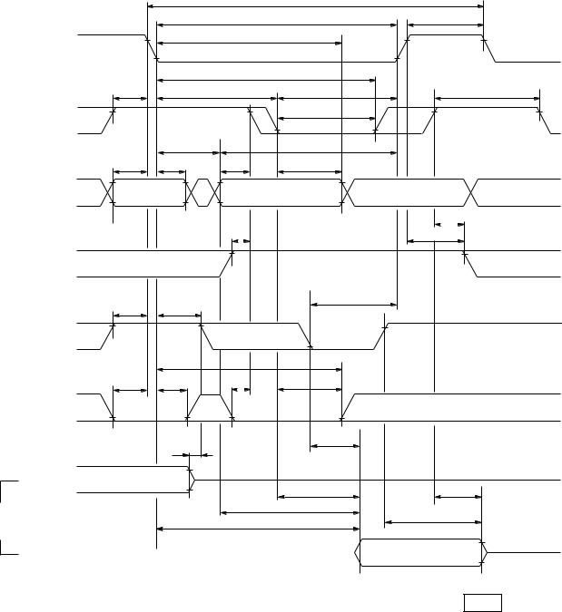
TIMING WAVEFORM
Read Cycle
|
|
|
|
|
tRC |
|
|
|
|
|
tRAS |
|
tRP |
RAS |
VIH – |
|
|
tAR |
|
|
VIL – |
|
|
|
|
|
|
|
|
|
tCSH |
|
|
|
|
|
|
|
|
|
|
|
|
tCRP |
|
tRCD |
tRSH |
tCPN |
CAS |
VIH – |
|
|
|
tCAS |
|
VIL – |
|
|
|
|
|
|
|
|
|
|
|
|
|
|
|
|
tRAD |
|
tRAL |
|
|
|
tASR |
tRAH |
tASC |
tCAH |
|
|
VIH – |
|
|
|
|
|
A0 - A8 VIL – |
Row Address |
Column Address |
tRCH |
|||
|
|
|
|
|
|
|
tRCS |
|
|
||
tRRH |
||||
|
|
|
|
|
|
VIH – |
|
|
|
|
WB/WE VIL – |
|
|
|
|
|
|
tTHS |
tTHH |
|
tROH |
|
|
|
|
|
||
DT/OE |
VIH – |
|
|
|
|
VIL – |
|
|
|
|
|
|
|
|
tFHR |
|
|
|
tFSR |
tRFH |
tFSC |
tCFH |
|
|
VIH – |
|
|
|
|
DSF VIL – |
|
|
|
|
|
|
|
tDZO |
|
tOEA |
|
|
|
|
|
|
|
|
VIH – |
|
|
|
|
IN VIL – |
|
|
tCAC |
tOFF |
|
W1/IO1 - |
|
tRAC |
|
tAA |
tOEZ |
|
|
|
|||
W8/IO8 |
|
|
|
|
|
|
|
|
|
|
|
VOH– |
|
Open |
|
|
|
Valid Data-out |
|
|
|
|
|||
OUT VOL – |
|
|
|
|
||
|
|
|
||||
|
|
|
|
|
||
|
|
|
|
|
|
"H" or "L"
10/45
¡ Semiconductor |
MSM518122 |
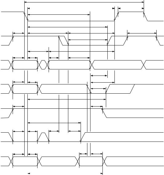
Write Cycle (Early Write) |
|
|
|
|||
|
|
|
|
|
tRC |
|
|
|
|
|
tRAS |
|
tRP |
RAS |
VIH – |
|
|
tAR |
|
|
VIL – |
|
|
|
|
|
|
|
|
|
tCSH |
|
|
|
|
|
|
|
|
|
|
|
|
tCRP |
|
tRCD |
tRSH |
tCPN |
CAS |
VIH – |
|
|
|
tCAS |
|
VIL – |
|
|
|
|
|
|
|
|
tRAD |
|
|
|
|
|
|
|
|
tRAL |
|
|
|
|
tASR |
tRAH |
tASC |
tCAH |
|
A0 - A8 |
VIH – |
Row Address |
Column Address |
|
||
VIL – |
|
|||||
|
|
|
|
|
|
|
|
|
tWSR |
tRWH |
tWCS |
tWCH |
|
|
VIH – |
|
*1 |
tWP |
|
|
WB/WE VIL – |
|
|
|
|
||
|
|
|
|
tWCR |
tCWL |
|
|
|
tTHS |
tTHH |
|
|
|
|
VIH – |
|
tRWL |
|
||
DT/OE |
|
|
|
|
|
|
VIL – |
|
|
|
|
|
|
|
|
|
|
tFHR |
|
|
|
|
tFSR |
tRFH |
tFSC |
tCFH |
|
|
VIH – |
|
|
|
|
|
DSF VIL – |
|
|
|
|
|
|
|
|
tMS |
tMH |
tDS |
tDH |
|
|
|
IN |
VIH – |
|
WM1 Data |
|
|
|
Valid Data-in |
|
|||||
|
|
|
|
|
|
|
|||||||||
|
|
VIL – |
|
|
|
|
|
||||||||
|
|
|
|
|
|
|
|
|
|
|
|
|
|||
|
|
|
|
|
|
|
tDHR |
|
|||||||
|
|
|
|
|
|
|
|
|
|
|
|
|
|||
W1/IO1 - |
|
|
|
|
|
|
|
||||||||
|
|
|
|
|
|
|
|
|
|
|
|
|
|||
W8/IO8 |
VOH– |
|
|
|
|
|
|
|
|
||||||
|
|
OUT |
|
|
|
|
Open |
|
|
||||||
|
|
|
|
|
|
|
|
||||||||
|
|
VOL – |
|
|
|
|
|
|
|||||||
|
|
|
|||||||||||||
|
|
|
|
|
|
|
|
|
|||||||
"H" or "L"
*1 WB/WE |
W1/IO1 - W8/IO8 |
Cycle |
|
|
|
|
|
|
0 |
WM1 data |
Write per Bit |
|
|
|
1 |
Don’t Care |
Normal Write |
|
|
|
WM1 data: |
0: Write Disable |
|
|
1: Write Enable |
|
11/45
¡ Semiconductor |
MSM518122 |
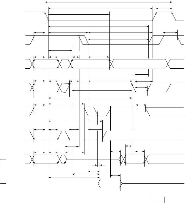
Write Cycle (OE Controlled Write)
tRC
tRAS |
|
tRP |
RAS |
VIH – |
|
|
tAR |
|
|
|
VIL – |
|
|
|
|
|
|
|
|
|
|
|
tCSH |
|
|
|
|
|
|
|
|
|
|
|
|
|
tCRP |
|
tRCD |
tRSH |
|
tCPN |
CAS |
VIH – |
|
|
|
tCAS |
|
|
VIL – |
|
|
|
|
|
|
|
|
|
tRAD |
|
tRAL |
|
|
|
|
|
|
|
|
|
||
|
|
tASR |
tRAH |
tASC |
tCAH |
|
|
|
VIH – |
|
|
|
|
|
|
A0 - A8 VIL – |
Row Address |
Column Address |
tCWL |
||||
|
|
|
|
|
|
||
|
|
tWSR |
tRWH |
|
|
|
tRWL |
|
VIH – |
|
*1 |
|
|
t |
WP |
WB/WE VIL – |
|
|
|
|
|||
|
|
|
tWCR |
|
|
||
|
|
|
|
|
|
|
|
|
|
tTHS |
|
|
|
tOEH |
|
DT/OE |
VIH – |
|
|
|
|
|
|
VIL – |
|
|
tFHR |
|
|
|
|
|
|
|
|
|
|
|
|
|
VIH – |
tFSR |
tRFH |
tFSC |
tCFH |
|
|
DSF VIL – |
|
|
|
|
|
|
|
|
|
tMS |
tMH |
|
tDS |
tDH |
|
|
|
VIH – |
|
WM1 Data |
|
|
|
|
|
|
|
|
|
|
|
|||
|
|
|
|
|
|
|
|
|
|
|
|
|
|
|||||
|
|
IN VIL – |
|
|
|
|
|
Valid Data-in |
||||||||||
|
|
|||||||||||||||||
|
|
|
|
|
|
|
tDHR |
|
|
|
|
|
|
|
||||
|
|
|
|
|
|
|
|
|
|
|||||||||
W1/IO1 - |
|
|
|
|
||||||||||||||
|
|
|
|
|
|
|
|
|||||||||||
W8/IO8 |
|
|
|
|
|
|
|
|
|
|
|
|
|
|
|
|||
|
|
VOH– |
|
|
|
|
|
|
|
Open |
|
|
|
|
|
|
||
|
|
|
|
|
|
|
|
|
|
|
|
|
|
|||||
|
|
OUT VOL – |
|
|
|
|
|
|
|
|||||||||
|
|
|
|
|
|
|||||||||||||
|
|
|
|
|
|
|
|
|
|
|
|
|
|
|
|
|
||
|
|
|
|
|
|
|
|
|
|
|
|
|
|
|
|
|
|
"H" or "L" |
|
|
|
|
|
|
|
|
|
|
|
|
|
|
|
|
|
|
|
|
|
|
|
|
|
|
|
|
|
|
|
|
|
|
|
|
|
|
*1 WB/WE |
W1/IO1 - W8/IO8 |
Cycle |
|
|
|
|
|
|
0 |
WM1 data |
Write per Bit |
|
|
|
1 |
Don’t Care |
Normal Write |
|
|
|
WM1 data: |
0: Write Disable |
|
|
1: Write Enable |
|
12/45
¡ Semiconductor |
MSM518122 |
Read Modify Write Cycle |
|
|
|
|
|||
|
|
|
|
|
|
tRWC |
|
|
|
|
|
|
tRAS |
|
tRP |
RAS |
VIH – |
|
|
tAR |
|
|
|
VIL – |
|
|
|
|
|
|
|
|
|
|
|
|
|
|
|
|
|
|
|
|
tCSH |
|
|
|
|
tCRP |
|
tRCD |
|
tRSH |
tCPN |
CAS |
VIH – |
|
|
|
|
tCAS |
|
|
VIL – |
|
|
|
|
|
|
|
|
|
|
tRAD |
|
|
|
|
|
tASR |
tRAH |
tASC |
tCAH |
|
|
A0 - A8 |
VIH – |
Row Address |
Column Address |
|
|
||
VIL – |
|
|
|||||
|
|
|
|
|
|
|
|
|
|
|
|
|
|
|
tCWL |
|
VIH – |
tWSR |
tRWH |
tRCS |
|
tCWD |
tRWL |
|
|
|
|
|
|
tWP |
|
WB/WE VIL – |
|
*1 |
|
tAWD |
|
|
|
|
|
|
|
|
tRWD |
|
|
|
|
tTHS |
|
tTHH |
|
|
tOEH |
DT/OE |
VIH – |
|
|
|
|
|
|
VIL – |
|
|
tFHR |
|
|
|
|
|
|
|
|
|
|
|
|
|
|
tFSR |
tRFH |
tFSC |
tCFH |
|
|
|
VIH – |
|
|
|
|
|
|
DSF VIL – |
|
|
|
|
|
tDS |
|
|
|
|
|
tDZC |
|
tOED |
|
|
|
tMS |
tMH |
tDZO |
|
tDH |
|
|
VIH – |
|
|
|
|
|
Valid |
IN VIL – |
WM1 Data |
|
tOEA |
|
Data-in |
||
W1/IO1 - |
|
|
|
tAA |
tCAC |
tOEZ |
|
W8/IO8 |
|
|
|
|
|
||
|
|
|
tRAC |
|
|
|
|
VOH– |
|
|
|
|
|
Valid |
|
|
|
|
|
||
OUT VOL – |
|
Open |
|
|
|
Data-out |
|
|
|||||
|
|
|
|
|
"H" or "L"
*1 WB/WE |
W1/IO1 - W8/IO8 |
Cycle |
|
|
|
|
|
|
0 |
WM1 data |
Write per Bit |
|
|
|
1 |
Don’t Care |
Normal Write |
|
|
|
WM1 data: |
0: Write Disable |
|
|
1: Write Enable |
|
13/45

¡ Semiconductor |
MSM518122 |
Fast Page Mode Read Cycle |
|
|
|
|
|
|
|
|
|||||
|
|
|
|
|
|
|
|
tRASP |
|
|
|
tRP |
|
RAS |
VIH – |
|
|
|
tAR |
|
|
tPC |
|
|
|
|
|
VIL – |
|
|
|
|
|
|
|
|
|
|
|
|
|
|
|
|
|
|
|
|
|
|
|
|
|
|
|
|
|
tCRP |
|
|
|
|
|
|
|
|
tRSH |
|
|
|
|
|
|
tRCD |
|
|
tCP |
t |
CP |
tCAS |
t |
CPN |
|
|
VIH – |
|
|
|
|
|
tCAS |
tCAS |
|
|
|||
CAS |
|
|
tRAD |
|
|
|
|
|
|
||||
VIL – |
|
|
|
tCSH |
|
|
|
|
|
tRAL |
|
|
|
|
|
|
|
|
|
|
tCAH |
|
|
|
|
||
|
|
tASR |
tRAH |
tASC |
t |
|
|
tASC |
|
|
|||
|
|
CAH |
tASC |
|
tCAH |
|
|
||||||
|
|
|
|
|
|
|
|
|
|
|
|
||
A0 - A8 |
VIH – |
Row |
|
|
|
Column |
Column |
|
|
Column |
|
|
|
VIL – |
|
|
|
|
|
|
|
||||||
|
Address |
|
|
Address 1 |
Address 2 |
|
|
Address n |
|
|
|||
|
|
|
|
|
|
|
|
|
|
|
tRCH |
||
|
|
|
|
|
|
|
tRCH |
|
tRCH |
|
|
||
|
|
|
|
|
tRCS |
|
tRCS |
|
tRCS |
tRRH |
|||
|
|
|
|
|
|
|
|
|
|||||
|
VIH – |
|
|
|
|
|
|
|
|
|
|
|
|
WB/WE VIL – |
|
|
|
|
|
|
|
|
|
|
|
|
|
|
tTHS |
tTHH |
|
|
|
|
|
|
|
|
DT/OE |
VIH – |
|
|
|
|
|
|
|
|
|
VIL – |
|
|
|
|
|
|
|
|
|
|
|
|
tFSC |
|
tFSC |
|
tFSC |
|
|
|
|
|
tFSR |
|
|
|
|
|
|
|||
|
tTHH |
tCFH |
|
tCFH |
|
|
tCFH |
|
|
|
|
VIH – |
|
|
|
|
|
||||
DSF VIL – |
tFHR |
|
|
|
|
|
|
|
|
|
|
|
|
|
|
|
|
|
|
|
|
|
|
tDZO |
|
tCPA |
|
|
tCPA |
|
|
|
|
VIH – |
|
|
|
|
|
|
|
||
IN VIL – |
|
tOEA |
tOFF |
tOEA |
|
tOEA |
t |
|
||
|
|
tCAC |
tCAC |
t |
OFF |
tCAC |
OFF |
|||
W1/IO1 - |
|
|
|
|
||||||
|
tAA |
|
tOEZ |
tOEZ |
tOEZ |
|||||
W8/IO8 |
|
|
tAA |
tAA |
||||||
VOH– |
tRAC |
|
|
|
|
|
|
|||
|
Open |
|
|
|
|
|
|
|
|
|
OUT VOL – |
Data-out 1 |
|
Data-out 2 |
Data-out n |
||||||
"H" or "L"
14/45
 Loading...