


OKI MSM51V18165B-50TS-K, MSM51V18165BSL-70JS, MSM51V18165BSL-70TS-K, MSM51V18165BSL-60JS, MSM51V18165B-70TS-K Datasheet
...¡SemiconductorSemiconductor MSM51V18165B/BSL
E2G0087-17-41
MSM51V18165B/BSL
1,048,576-Word ´ 16-Bit DYNAMIC RAM : FAST PAGE MODE TYPE WITH EDO
DESCRIPTION
TheMSM51V18165B/BSLisa1,048,576-word´ 16-bitdynamicRAMfabricatedinOki'ssilicon-gate CMOStechnology.TheMSM51V18165B/BSLachieveshighintegration,high-speedoperation,and low-power consumption because Oki manufactures the device in a quadruple-layer polysilicon/ double-layer metal CMOS process. The MSM51V18165B/BSL is available in a 42-pin plastic SOJ or 50/44-pin plastic TSOP. The MSM51V18165BSL (the self-refresh version) is specially designed for lower-power applications.
FEATURES
•1,048,576-word ´ 16-bit configuration
•Single 3.3 V power supply, ±0.3 V tolerance
• Input : LVTTL compatible, low input capacitance
•Output : LVTTL compatible, 3-state
•Refresh : 1024 cycles/16 ms, 1024 cycles/128 ms (SL version)
•Fast page mode with EDO, read modify write capability
•CAS before RAS refresh, hidden refresh, RAS-only refresh capability
•CAS before RAS self-refresh capability (SL version)
•Package options:
42-pin 400 mil plastic SOJ |
(SOJ42-P-400-1.27) |
(Product : MSM51V18165B/BSL-xxJS) |
50/44-pin 400 mil plastic TSOP |
(TSOPII50/44-P-400-0.80-K) (Product : MSM51V18165B/BSL-xxTS-K) |
|
|
|
xx indicates speed rank. |
PRODUCT FAMILY
Family |
Access Time (Max.) |
Cycle Time |
Power Dissipation |
|
|||||
|
|
|
|
(Min.) |
|
|
|
||
tRAC |
tAA |
tCAC |
tOEA |
Operating (Max.) |
Standby (Max.) |
|
|||
|
|||||||||
|
|
||||||||
MSM51V18165B/BSL-50 |
50 ns |
25 ns |
13 ns |
13 ns |
84 ns |
684 mW |
1.8 mW/ |
||
|
|
|
|
|
|
|
|||
MSM51V18165B/BSL-60 |
60 ns |
30 ns |
15 ns |
15 ns |
104 ns |
576 mW |
|||
0.72 mW (SL version) |
|||||||||
|
|
|
|
|
|
|
|||
MSM51V18165B/BSL-70 |
70 ns |
35 ns |
20 ns |
20 ns |
124 ns |
504 mW |
|||
|
|
||||||||
|
|
|
|
|
|
|
|
|
|
409
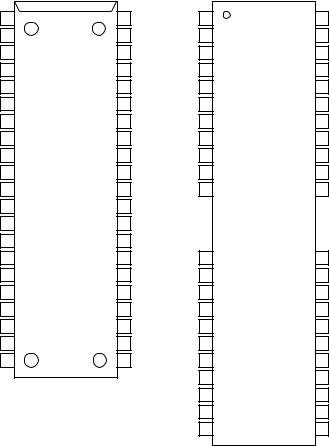
MSM51V18165B/BSL |
¡ Semiconductor |
PIN CONFIGURATION (TOP VIEW) |
|
|
|
|
|
||
VCC |
1 |
42 |
VSS |
VCC |
1 |
50 |
VSS |
DQ1 |
2 |
41 |
DQ16 |
DQ1 |
2 |
49 |
DQ16 |
DQ2 |
3 |
40 |
DQ15 |
DQ2 |
3 |
48 |
DQ15 |
DQ3 |
4 |
39 |
DQ14 |
DQ3 |
4 |
47 |
DQ14 |
DQ4 |
5 |
38 |
DQ13 |
DQ4 |
5 |
46 |
DQ13 |
VCC |
6 |
37 |
VSS |
VCC |
6 |
45 |
VSS |
DQ5 |
7 |
36 |
DQ12 |
DQ5 |
7 |
44 |
DQ12 |
DQ6 |
8 |
35 |
DQ11 |
DQ6 |
8 |
43 |
DQ11 |
DQ7 |
9 |
34 |
DQ10 |
DQ7 |
9 |
42 |
DQ10 |
DQ8 10 |
33 |
DQ9 |
DQ8 10 |
41 |
DQ9 |
||
NC 11 |
32 |
NC |
NC 11 |
40 |
NC |
||
NC 12 |
31 |
LCAS |
|
|
|
|
|
WE 13 |
30 |
UCAS |
|
|
|
|
|
RAS 14 |
29 |
OE |
|
|
|
|
|
NC 15 |
28 |
A9 |
NC 15 |
36 |
NC |
||
NC 16 |
27 |
A8 |
NC 16 |
35 |
LCAS |
||
A0 |
17 |
26 |
A7 |
WE 17 |
34 |
UCAS |
|
A1 |
18 |
25 |
A6 |
RAS 18 |
33 |
OE |
|
A2 |
19 |
24 |
A5 |
NC 19 |
32 |
A9 |
|
A3 |
20 |
23 |
A4 |
NC 20 |
31 |
A8 |
|
VCC 21 |
22 |
VSS |
A0 |
21 |
30 |
A7 |
|
|
42-Pin Plastic SOJ |
|
|
A1 |
22 |
29 |
A6 |
|
|
|
A2 |
23 |
28 |
A5 |
|
|
|
|
|
A3 |
24 |
27 |
A4 |
|
|
|
|
VCC 25 |
26 |
VSS |
|
50/44-Pin Plastic TSOP
(K Type)
Pin Name |
Function |
|
|
A0 - A9 |
Address Input |
|
|
RAS |
Row Address Strobe |
LCAS |
Lower Byte Column Address Strobe |
|
|
UCAS |
Upper Byte Column Address Strobe |
DQ1 - DQ16 |
Data Input/Data Output |
|
|
OE |
Output Enable |
|
|
WE |
Write Enable |
VCC |
Power Supply (3.3 V) |
VSS |
Ground (0 V) |
NC |
No Connection |
Note : The same power supply voltage must be provided to every VCC pin, and the same GND voltage level must be provided to every VSS pin.
410

¡ Semiconductor MSM51V18165B/BSL
BLOCK DIAGRAM
|
Timing |
|
|
|
WE |
OE |
|
|
|
|
|
RAS |
|
|
|
|
|
|
|
|
|
||
Generator |
|
|
|
|
|
|
|
|
|
||
LCAS |
|
|
|
|
|
|
I/O |
|
|
|
|
|
|
|
|
|
|
Controller |
|
|
Output |
|
|
UCAS |
|
|
|
|
|
|
|
|
8 |
8 |
|
|
|
|
|
|
|
I/O |
|
Buffers |
|||
|
|
|
|
|
|
|
Controller |
|
|
|
DQ1 - DQ8 |
|
|
|
|
|
|
|
|
|
|
|
|
|
10 |
Column |
|
|
|
10 |
Column Decoders |
|
|
Input |
|
|
Address |
|
|
|
|
8 |
8 |
||||
|
|
Buffers |
|
|
|
|
|
|
|
Buffers |
|
|
|
|
|
|
|
|
|
|
|
|
|
|
|
Internal |
|
|
|
Sense Amplifiers 16 |
I/O |
16 |
|
|
|
A0 - A9 |
|
|
Refresh |
|
Selector |
|
|
||||
|
Address |
|
|
|
|
|
|
|
|||
|
|
Counter |
|
Control Clock |
|
|
|
|
|
|
|
|
|
|
|
|
|
|
|
|
|
|
|
|
|
|
|
|
|
|
|
|
8 |
Input |
8 |
|
|
Row |
|
|
|
|
|
|
Buffers |
||
|
|
|
Row |
|
|
|
|
|
|
||
|
|
|
|
|
Memory |
|
|
|
|
||
|
10 |
Address |
10 |
|
|
|
|
|
DQ9 - DQ16 |
||
|
Deco- |
Word |
|
|
|
|
|||||
|
|
Buffers |
|
|
Cells |
|
|
|
|||
|
|
|
ders |
Drivers |
|
|
|
Output |
|
||
|
|
|
|
|
|
|
|
|
8 |
8 |
|
|
|
|
|
|
|
|
|
|
Buffers |
||
|
|
|
|
|
|
|
|
|
|
|
|
VCC
On Chip
VBB Generator
VSS
FUNCTION TABLE
|
|
Input Pin |
|
|
DQ Pin |
Function Mode |
||
RAS |
LCAS |
UCAS |
WE |
OE |
DQ1 - DQ8 DQ9 - DQ16 |
|||
|
||||||||
|
|
|
|
|
|
|
|
|
H |
* |
* |
* |
* |
High-Z |
High-Z |
Standby |
|
L |
H |
H |
* |
* |
High-Z |
High-Z |
Refresh |
|
L |
L |
H |
H |
L |
DOUT |
High-Z |
Lower Byte Read |
|
L |
H |
L |
H |
L |
High-Z |
DOUT |
Upper Byte Read |
|
L |
L |
L |
H |
L |
DOUT |
DOUT |
Word Read |
|
L |
L |
H |
L |
H |
DIN |
Don't Care |
Lower Byte Write |
|
L |
H |
L |
L |
H |
Don't Care |
DIN |
Upper Byte Write |
|
L |
L |
L |
L |
H |
DIN |
DIN |
Word Write |
|
L |
L |
L |
H |
H |
High-Z |
High-Z |
— |
|
*: "H" or "L"
411
 Loading...