


OKI MSM65P524-xxxGS-BK, MSM65P524-xxxJS, MSM65P524-xxxSS, MSM65524A-xxxSS, MSM65524A-xxxGS-BK Datasheet
...E2E1016-27-Y6
This version: Jan. 1998
Semiconductor MSM65524A/65P524
¡ Semiconductor
Previous version: Nov. 1996
MSM65524A/65P524
8-Bit Microcontroller with A/D Converter
GENERAL DESCRIPTION
The MSM65524A is a high-performance 8-bit microcontroller that employs OKI original nX-8/ 50 CPU core. With a minimum instruction execution time of 400 ns (10MHz clock), the MSM65524A is capable of high-speed processing, and includes 16K bytes of program memory, 384 bytes of data memory, timers, serial ports, an A/D converter and PWMs on chip. Also available are the MSM65P524, which replaces the on-chip program memory with one-time PROM, and the MSM65X524A, which uses the external program memory.
FEATURES
• Operating range |
|
|
Operating frequency |
: 0 to 10MHz (VDD=4.5 to 5.5V) |
|
|
|
0 to 5MHz (VDD=2.7 to 5.5V) |
Operating voltage |
: |
2.7 to 5.5V |
Operating temperature |
: |
–40 to +85°C |
• Memory space |
: |
64K bytes |
Internal program memory |
: |
16K bytes |
Internal data memory |
: |
384 bytes |
• Minimum instruction execution time |
: 400ns @ 10 MHz |
|
• Powerful instruction set |
: |
83 basic instructions |
|
|
8/16-bit operation instructions |
|
|
Bit manipulation instructions |
|
|
Compound function instructions |
• Abundant addressing modes |
: 8 ´ 8 ® 16 |
|
• Multiplication/division operation functions |
||
|
|
16 ÷ 8 ® 16 ... 8 |
• I/O port |
: 5 ports ´ 8 bits |
|
Input-output port |
||
|
|
1 port ´ 4 bits |
Input port |
: 1 port ´ 8 bits |
|
• Timers |
: 8-bit auto-reload timer ´ 2 |
|
|
|
16-bit auto-reload timer ´ 1 |
|
|
Watchdog timer ´ 1 |
• Counters |
: Time base counter ´ 1 |
|
|
|
16-bit free-running counter ´ 1 |
• Capture input |
: |
1 channel |
• Compare output |
: |
2 channels |
• Serial ports |
: Shift register ´ 1 |
|
|
|
Serial port with baud rate generator |
|
|
(UART/Synchronous) ´ 1 |
• A/D converter |
: 8 bits ´ 8 channels |
|
• PWM |
: |
8 bits ´ 2 channels |
PWM with auto-reload timer for period setting
1/27
¡ Semiconductor |
|
MSM65524A/65P524 |
||
|
|
|
|
|
• External interrupts |
: |
3 |
|
|
• Interrupt sources |
: |
19 |
|
|
• Package options |
|
(Product name: MSM65524A-´´´SS, |
||
|
64-pin plastic shrink DIP (SDIP64-P-750-1.78) : |
|||
|
|
|
MSM65P524-´´´SS) |
|
|
64-pin plastic QFP (QFP64-P-1414-0.80-BK) |
: |
(Product name: MSM65524A-´´´GS-BK, |
|
|
|
|
MSM65P524-´´´GS-BK) |
|
|
68-pin plastic QFJ (PLCC) (QFJ68-P-S950-1.27): |
(Product name: MSM65524A-´´´JS, |
||
|
|
|
MSM65P524-´´´JS) |
|
|
|
|
´´´ indicates the code number. |
|
2/27

3/27
OSC 0
OSC 1
RESET
HSTOP*
VDD
GND
|
|
|
|
ROM |
8 |
|
|
|
(16K bytes) |
||
|
|
|
|
||
OSC |
CPU CORE |
|
|
|
|
CONT. |
|
|
|
|
|
|
|
|
|
|
|
|
INST. |
|
8 |
|
|
|
DEC. |
|
|
|
|
|
|
|
|
|
|
|
|
ALU |
|
GMAR |
|
T/C |
|
|
PC |
|
|
|
|
|
|
||
|
IR |
|
|
|
BUS |
|
|
|
|
CONT. |
|
|
|
|
|
|
|
|
|
8 |
|
|
|
AR |
BR |
PSW |
SP |
LMAR |
|
MUL/DIV |
8-bit A/D C ´ 8ch |
I/O PORT |
AV |
V |
V |
AGND |
-AI0* |
P0 |
P1 |
P2 |
P3 |
P4 |
P5 |
P6 |
DD |
RH |
RL |
|||||||||
|
|
|
|
|
|||||||
|
|
|
|
AI7* |
|
|
|
|
|
|
|
EXT.MEM. |
8 |
AD0-7* |
CONT. |
8 |
A8-15* |
|
|
RD |
|
|
WR* |
|
|
ALE |
|
|
EA |
RAM (384 bytes)
TBC  WDT
WDT
16-bit TIMER |
|
|
|
T2CK* |
|
|
|
|
|||
|
|
|
|
|
CAP* |
16-bit FRC |
|
|
|
CMP0* |
|
CAP´1, CMP´2 |
|
|
|
CMP1* |
|
|
|
|
|||
SIO |
|
|
|
TXD* |
|
|
|
|
RXD* |
||
|
|
|
|
|
|
8-bit PWM´2 |
|
|
|
PWM0* |
|
|
|
|
PWM1* |
||
|
|
|
|||
8-bit TIMER´4** |
|
|
|
T1OUT* |
|
|
|
|
T0CK* |
||
|
|
|
|
|
GATE* |
|
|
|
|
|
|
|
|
|
|
|
SFTO* |
8-bit SHIFT-REG. |
|
|
|
SFTI* |
|
|
|
|
|||
|
|
|
|
|
SFTCK* |
|
|
|
|
|
|
|
|
|
|
|
|
|
|
|
|
|
INT0* |
|
|
|
|
|
|
|
|
|
|
|
|
INTERRUPT CONT.  INT1*
INT1*
 INT2*
INT2*
* Secondary functions of ports
**One timer doubles as the SIO baud rate generator, another doubles as a PWM clock source.
DIAGRAM BLOCK |
Semiconductor ¡ |
MSM65524A/65P524

¡ Semiconductor |
MSM65524A/65P524 |
||
|
|
|
|
PIN CONFIGURATION (TOP VIEW)
|
|
|
|
|
P5.0/PWM0 |
1 |
|
64 |
VDD |
P5.1/PWM1 |
|
|
|
AVDD |
2 |
63 |
|||
P5.2 |
|
|
|
VRH |
3 |
62 |
|||
P5.3 |
|
|
|
VRL |
4 |
61 |
|||
P4.0 |
|
|
|
P6.7/AI7 |
5 |
60 |
|||
P4.1 |
|
|
|
P6.6/AI6 |
6 |
59 |
|||
P4.2 |
|
|
|
P6.5/AI5 |
7 |
58 |
|||
P4.3 |
|
|
|
P6.4/AI4 |
8 |
57 |
|||
P4.4 |
|
|
|
P6.3/AI3 |
9 |
56 |
|||
P4.5 |
|
|
|
P6.2/AI2 |
10 |
55 |
|||
P4.6 |
|
|
|
P6.1/AI1 |
11 |
54 |
|||
P4.7 |
|
|
|
P6.0/AI0 |
12 |
53 |
|||
P3.0/T2CK |
|
|
|
AGND |
13 |
52 |
|||
P3.1/CAP |
|
|
|
P0.0/AD0 |
14 |
51 |
|||
P3.2/CMP0 |
|
|
|
P0.1/AD1 |
15 |
50 |
|||
P3.3/CMP1 |
|
|
|
P0.2/AD2 |
16 |
49 |
|||
P3.4/INT2 |
|
|
|
P0.3/AD3 |
17 |
48 |
|||
P3.5/SFTO |
|
|
|
P0.4/AD4 |
18 |
47 |
|||
P3.6/SFTI |
|
|
|
P0.5/AD5 |
19 |
46 |
|||
P3.7/SFTCK |
|
|
|
P0.6/AD6 |
20 |
45 |
|||
RESET |
|
|
|
P0.7/AD7 |
21 |
|
44 |
||
P2.0/RXD |
|
|
|
EA |
22 |
|
43 |
||
P2.1/TXD |
|
|
|
ALE |
23 |
|
42 |
||
P2.2/INT0 |
|
|
|
RD |
24 |
|
41 |
||
P2.3/INT1/GATE |
|
|
|
P1.7/A15 |
25 |
|
40 |
||
P2.4/T0CK |
|
|
|
P1.6/A14 |
26 |
|
39 |
||
P2.5/HSTOP |
|
|
|
P1.5/A13 |
27 |
|
38 |
||
P2.6/WR |
|
|
|
P1.4/A12 |
28 |
|
37 |
||
P2.7/T1OUT |
|
|
|
P1.3/A11 |
29 |
|
36 |
||
OSC1 |
|
|
|
P1.2/A10 |
30 |
|
35 |
||
OSC0 |
|
|
|
P1.1/A9 |
31 |
|
34 |
||
GND |
|
|
|
P1.0/A8 |
32 |
|
33 |
||
|
|
|
|
|
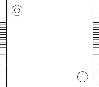
64-Pin Plastic Shrink DIP
4/27
¡ Semiconductor |
MSM65524A/65P524 |
||
|
|
|
|
PIN CONFIGURATION (TOP VIEW) (Continued)
P4.4 1
P4.5 2
P4.6 3
P4.7 4
P3.0/T2CK 5
P3.1/CAP 6
P3.2/CMP0 7
P3.3/CMP1 8
P3.4/INT2 9
P3.5/SFTO 10
P3.6/SFTI 11 P3.7/SFTCK 12
RESET 13 P2.0/RXD 14 P2.1/TXD 15 P2.2/INT0 16
|
P4.3 |
|
P4.2 |
|
P4.1 |
|
P4.0 |
|
P5.3 |
|
P5.2 |
|
P5.1/PWM1 |
P5.0/PWM0 |
|
V |
|
AV |
|
V |
|
V |
|
P6.7/AI7 |
|
P6.6/AI6 |
|
P6.5/AI5 |
|
P6.4/AI4 |
||
|
|
|
|
|
|
|
|
|
|
|
|
|
|
|
|
|
DD |
|
DD |
|
RH |
|
RL |
|
|
|
|
|
|
|
|
|
|
|
|
|
|
|
|
|
|
|
|
|
|
|
|
|
|
|
|
|
|
|
|
|
|
|
|
|
|
|
|
|
|
|
64 |
|
63 |
|
62 |
|
61 |
|
60 |
|
59 |
|
58 |
|
57 |
|
56 |
|
55 |
|
54 |
|
53 |
|
52 |
|
54 |
|
50 |
|
49 |
|
|
|
|
|
|
|
|
|
|
|
|
|
|
|
|
|
|
|
|
|
|
|
|
|
|
|
|
|
|
|
|
|
|
|
17 |
|
18 |
|
19 |
|
20 |
|
21 |
|
22 |
|
23 |
|
24 |
|
25 |
|
26 |
|
27 |
|
28 |
|
29 |
|
30 |
|
31 |
|
32 |
|
|
|
|
|
|
|
|
|
|
|
|
|
|
|
|
|
|
|
|
|
|
|
|
|
|
|
|
|
|
|
|
|
|
|
P2.3/INT1/GATE |
|
P2.4/T0CK |
P2.5/HSTOP |
P2.6/WR |
|
P2.7/T1OUT |
OSC1 |
|
OSC0 |
|
GND |
|
P1.0/A8 |
|
P1.1/A9 |
|
P1.2/A10 |
|
P1.3/A11 |
|
P1.4/A12 |
|
P1.5/A13 |
|
P1.6/A14 |
|
P1.7/A15 |
|
|||
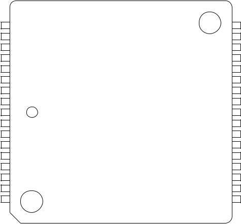
64-Pin Plastic QFP
48 P6.3/AI3
47 P6.2/AI2
46 P6.1/AI1
45 P6.0/AI0
44 AGND
43 P0.0/AD0
42 P0.1/AD1
41 P0.2/AD2
40 P0.3/AD3
39 P0.4/AD4
38 P0.5/AD5
37 P0.6/AD6
36 P0.7/AD7
35 EA
34 ALE
33 RD
5/27
¡ Semiconductor |
MSM65524A/65P524 |
||
|
|
|
|
PIN CONFIGURATION (TOP VIEW) (Continued)
P6.4/AI4 61 P6.5/AI5 62 P6.6/AI6 63 P6.7/AI7 64 VRL 65 VRH 66 AVDD 67 NC 68 VDD 1
P5.0/PWM0 2 P5.1/PWM1 3 P5.2 4 P5.3 5 P4.0 6 P4.1 7 P4.2 8 P4.3 9
P6.3/AI3 |
|
P6.2/AI2 |
|
P6.1/AI1 |
|
P6.0/AI0 |
|
AGND |
|
P0.0/AD0 |
|
P0.1/AD1 |
|
P0.2/AD2 |
|
NC |
|
P0.3/AD3 |
|
P0.4/AD4 |
|
P0.5/AD5 |
|
P0.6/AD6 |
|
P0.7/AD7 |
EA |
|
ALE |
RD |
||
|
|
|
|
|
|
|
|
|
|
|
|
|
|
|
|
|
|
|
|
|
|
|
|
|
|
|
|
|
|
|
|
|
60 |
|
59 |
|
58 |
|
57 |
|
56 |
|
55 |
|
54 |
|
53 |
|
52 |
|
51 |
|
50 |
|
49 |
|
48 |
|
47 |
|
46 |
|
45 |
|
44 |
|
|
|
|
|
|
|
|
|
|
|
|
|
|
|
|
|
|
|
|
|
|
|
|
|
|
|
|
|
|
|
|
|
10 |
|
11 |
|
12 |
|
13 |
|
14 |
|
15 |
|
16 |
|
17 |
|
18 |
|
19 |
|
20 |
|
21 |
|
22 |
|
23 |
|
24 |
|
25 |
|
26 |
P4.4 |
|
P4.5 |
|
P4.6 |
|
P4.7 |
|
P3.0/T2CK |
|
P3.1/CAP |
|
P3.2/CMP0 |
|
P3.3/CMP1 |
NC |
|
P3.4/INT2 |
|
P3.5/SFTO |
|
P3.6/SFTI |
|
P3.7/SFTCK |
RESET |
|
P2.0/RXD |
|
P2.1/TXD |
|
P2.2/INT0 |
||
NC: No-connection pin
68-Pin Plastic QFJ (PLCC)
43 |
P1.7/A15 |
42 |
P1.6/A14 |
41 |
P1.5/A13 |
40 |
P1.4/A12 |
39 |
P1.3/A11 |
38 |
P1.2/A10 |
37 |
P1.1/A9 |
36 |
P1.0/A8 |
35 |
NC |
34 |
GND |
33 |
OSC0 |
32 |
OSC1 |
31 |
P2.7/T1OUT |
30 |
P2.6/WR |
29 |
P2.5/HSTOP |
28 |
P2.4/T0CK |
27 |
P2.3/INT1/GATE |
6/27

¡ Semiconductor MSM65524A/65P524
PIN DESCRIPTION
Basic Functions
Function |
Symbol |
Type |
Description |
|
|
|
|
|
|
|
|
|
VDD |
— |
+5V digital power supply |
|
|
|
GND |
— |
0V digital ground |
|
|
Power |
AVDD |
— |
+5V analog power supply |
|
|
Supply |
AGND |
— |
0V analog ground |
|
|
|
|||||
|
VRH |
— |
+5V analog reference voltage |
|
|
|
VRL |
— |
0V analog reference voltage |
||
|
|
|
|
|
|
|
OSC0 |
I |
System clock input pin. Quartz oscillator or ceramic oscillator is |
||
Oscillation |
|
|
connected between OSC0 and OSC1. For external clock, input at OSC0, |
||
|
|
leaving OSC1 open. |
|
||
|
|
|
|||
|
OSC1 |
O |
System clock output pin |
||
|
|
|
|
|
|
|
RESET |
I |
System reset input (program starts from address 0040H); |
||
|
|
|
internal pull-up resistance |
||
|
|
|
|
|
|
|
EA |
I |
Program memory select input pin. |
||
Control |
|
|
"L" level input for external program memory; "H" level input for internal |
||
|
|
|
program memory. |
||
|
|
|
|
|
|
|
RD |
O |
Read strobe signal during external memory access |
||
|
|
|
|
|
|
|
ALE |
O |
Address latch signal during external memory access |
||
|
|
|
|
|
|
|
PORT 0 |
I/O |
8-bit Input-output port |
||
|
|
|
During external memory access, becomes address/data bus for address |
||
|
|
|
output, instruction fetch or data read/write along with ALE, RD and WR |
||
|
|
|
pins. |
||
|
|
|
|
|
|
|
PORT 1 |
I/O |
8-bit Input-output port |
||
Port |
|
|
Address bus during external memory access |
||
|
|
|
|
||
PORT 2 |
I/O |
8-bit Input-output port ´ 3. Secondary functions shown in following table |
|||
|
|||||
|
PORT 3 |
|
are added for ports 2 and 3. |
||
|
PORT 4 |
|
|
|
|
|
|
|
|
|
|
|
PORT 5 |
I/O |
4-bit Input-output port |
||
|
|
|
Secondary functions shown in following table are added for port 5. |
||
|
|
|
|
|
|
|
PORT 6 |
I |
8-bit Input port |
||
|
|
|
Functions as analog input channel during A/D conversion. |
||
|
|
|
|
|
|
7/27
¡ Semiconductor |
MSM65524A/65P524 |
|||||
|
|
|
|
|
|
|
Secondary Functions |
|
|
||||
|
|
|
|
|
|
|
|
|
Symbol |
Type |
Description |
|
|
|
|
|
|
|
|
|
|
|
RXD |
I/O |
P2.0 secondary function |
|
|
|
|
|
|
UART: Input pin for serial port receive data. |
|
|
|
|
|
|
Synchronous: Input/output pin for serial port transmit/receive data. |
||
|
|
|
|
|
|
|
|
|
TXD |
O |
P2.1 secondary function |
|
|
|
|
|
|
UART: Output pin for serial port transmit data. |
|
|
|
|
|
|
Synchronous: Output pin for serial port synchronizing clock. |
||
|
|
|
|
|
|
|
|
|
INT0 |
I |
P2.2 secondary function |
|
|
|
|
|
|
External interrupt 0 input pin. |
|
|
|
|
|
|
|
|
|
|
|
INT1/GATE |
I |
P2.3 secondary functions |
|
|
|
|
|
|
External interrupt 1 input pin. Also used as input pin for gate signal |
||
|
|
|
|
for timer 0 count enable/disable. |
|
|
|
|
|
|
|
|
|
|
|
T0CK |
I |
P2.4 secondary function |
|
|
|
|
|
|
Timer 0 external clock input pin. |
|
|
|
|
|
|
|
|
|
|
|
HSTOP |
I |
P2.5 secondary function |
|
|
|
|
|
|
Hard stop mode input pin; stops system clock oscillation with "L" level input. |
||
|
|
|
|
|
|
|
|
|
WR |
O |
P2.6 secondary function |
|
|
|
|
|
|
Write strobe signal output pin during external data memory access. |
||
|
|
|
|
|
|
|
|
|
T1OUT |
O |
P2.7 secondary function |
|
|
|
|
|
|
Output pin for signal that 2-divided timer 1 overflow. |
|
|
|
|
|
|
|
|
|
|
|
T2CK |
I |
P3.0 secondary function |
|
|
|
|
|
|
Timer 2 external clock input pin. |
|
|
|
|
|
|
|
|
|
|
|
CAP |
I |
P3.1 secondary function |
|
|
|
|
|
|
Capture trigger input pin. |
|
|
|
|
|
|
|
|
|
|
|
CMP0 |
O |
P3.2 secondary function |
|
|
|
|
|
|
Compare output channel 0 output pin. |
|
|
|
|
|
|
|
|
|
|
|
CMP1 |
O |
P3.3 secondary function |
|
|
|
|
|
|
Compare output channel 1 output pin. |
|
|
|
|
|
|
|
|
|
|
|
INT2 |
I |
P3.4 secondary function |
|
|
|
|
|
|
External interrupt 2 input signal. |
|
|
|
|
|
|
|
|
|
|
|
SFTO |
O |
P3.5 secondary function |
|
|
|
|
|
|
Shift register data output pin. |
|
|
|
|
|
|
|
|
|
|
|
SFTI |
I |
P3.6 secondary function |
|
|
|
|
|
|
Shift register data input pin. |
|
|
|
|
|
|
|
|
|
|
|
SFTCK |
I/O |
P3.7 secondary function |
|
|
|
|
|
|
Shift register synchronizing clock input/output pin. |
|
|
|
|
|
|
|
|
|
|
|
PWM0 |
O |
P5.0 secondary function |
|
|
|
|
|
|
PWM channel 0 output pin. |
|
|
|
|
|
|
|
|
|
|
|
PWM1 |
O |
P5.1 secondary function |
|
|
|
|
|
|
PWM channel 1 output pin. |
|
|
|
|
|
|
|
|
|
8/27
¡ Semiconductor |
|
|
|
|
|
|
|
|
|
|
|
|
|
|
|
|
|
|
|
MSM65524A/65P524 |
|||||||
|
|
|
|
|
|
|
|
|
|
|
|
|
|
|
|
|
|
|
|
|
|
|
|
|
|
|
|
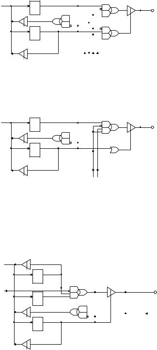
Port Circuit Configuration |
|
|
|
|
|
|
|
|
|
|
|
|
|
|
|
|
|
|
|
|
|
|
|
|
|||
|
|
|
|
|
|
|
|
|
|
|
|
|
|
|
|
|
|
|
|
|
|
|
|
|
|
|
|
|
Type |
Port |
|
Circuit Configuration |
|
|
|
Electrical Characteristics |
|||||||||||||||||||
|
|
|
|
|
(VDD=5V) |
|
|||||||||||||||||||||
|
|
|
|
|
|
|
|
|
|
|
|
|
|
|
|
|
|
|
|
|
|
|
|
|
|||
|
|
|
Data Bus |
|
|
|
|
|
|
|
|
|
|
|
|
|
|
|
|
|
|
|
|
|
"H" Input Voltage: |
||
|
|
|
P0D |
|
|
|
|
|
|
|
|
|
|
|
|
|
PORT0 |
• VIH=2.4V |
|||||||||
|
|
|
|
|
|
|
|
|
|
|
|
|
|
|
|
|
"L" Input Voltage: |
||||||||||
|
|
P0.0/AD0 to |
|
|
|
|
|
|
|
|
|
|
|
|
|
|
|
|
|
|
|
|
|
|
• VIL=0.8V |
||
|
|
|
|
|
|
|
|
|
|
|
|
|
|
|
|
|
|
|
|
|
|
|
|
||||
|
|
|
|
|
|
|
|
|
|
|
|
|
|
|
|
|
|
|
|
|
|
|
|
|
|
||
1 |
|
P0 |
|
|
|
|
|
|
|
|
|
|
|
|
|
|
|
"H" Output Voltage: |
|||||||||
|
|
|
|
|
|
|
|
|
|
|
|
|
|
|
|
||||||||||||
|
|
|
|
|
|||||||||||||||||||||||
P0.7/AD7 |
|
DIR |
|
|
|
|
|
|
|
|
|
|
|
|
|
||||||||||||
|
|
|
|
|
|
|
|
|
|
|
|
|
|
||||||||||||||
|
|
|
|
|
|
|
|
|
|
|
|
|
|
||||||||||||||
|
|
|
|
|
|
|
|
|
|
|
|
|
|
|
|
|
|
|
|
|
|
|
|
• VOH=3.75V |
|||
|
|
|
|
|
|
|
|
|
|
|
|
|
|
|
|
|
|
|
|
|
|
|
|
|
|||
|
|
|
|
|
|
|
|
|
|
|
|
|
|
|
|
|
|
|
|
|
|
|
|
|
• IOH=–400mA |
||
|
|
|
|
External Memory Control |
|
|
|
"L" Output Voltage: |
|||||||||||||||||||
|
|
|
|
|
|
|
|
|
|
|
|
|
|
|
|
|
|
|
|
|
|
|
|
|
• VOL=0.4V |
||
|
|
|
|
|
|
|
|
|
|
|
|
|
|
|
|
|
|
|
|
|
|
|
|
|
• IOL=3.2mA |
|
|
|
|
|
|
|
|
|
|
|
|
|
|
|
|
|
|
|
|
|
|
|
|
|
|
|
"H" Input Voltage: |
||
|
|
|
Data Bus |
|
|
|
|
|
|
|
|
|
|
|
|
|
|
|
|
|
|
|
PORT1 |
• VIH=2.4V |
|||
|
|
|
|
P1D |
|
|
|
|
|
|
|
|
"L" Input Voltage: |
||||||||||||||
|
|
|
|
|
|
||||||||||||||||||||||
|
|
P1.0/A8 to |
|
|
|
|
|
|
|
|
|
|
|
|
|
|
|
|
|
|
|
|
|
|
• VIL=0.8V |
||
|
|
|
|
|
|
|
|
|
|
|
|
|
|
|
|
|
|
|
|
|
|
|
|
||||
|
|
|
|
|
|
|
|
|
|
|
|
|
|
|
|
|
|
|
|
|
|||||||
|
|
|
|
|
|
|
|
|
|
|
|
|
|
|
|
|
|
|
|
||||||||
2 |
|
P1 |
|
|
|
|
|
|
|
|
|
|
"H" Output Voltage: |
||||||||||||||
|
|
|
|
|
|||||||||||||||||||||||
P1.7/A15 |
|
DIR |
|
|
|
|
|
|
|
|
|
||||||||||||||||
|
|
|
|
|
|
|
|
|
• VOH=3.75V |
||||||||||||||||||
|
|
|
|
|
|
|
|
|
|
|
|
|
|
|
|
|
|
|
|
|
|
|
|
|
|||
|
|
|
|
|
|
|
|
|
|
|
|
|
|
|
|
|
|
|
|
|
|
|
|
|
• IOH=–200mA |
||
|
|
|
|
External Memory Control |
|
|
|
"L" Output Voltage: |
|||||||||||||||||||
|
|
|
|
|
|
|
|
|
|
|
|
|
|
|
|
|
|
|
|
|
|
|
|
|
• VOL=0.4V |
||
|
|
|
|
|
|
|
|
|
|
|
|
|
|
|
|
|
|
|
|
|
|
|
|
|
• IOL=1.6mA |
||
|
|
|
|
|
|
|
|
|
|
|
|
|
|
|
|
|
|
|
|
|
|
|
|
|
|
|
|
|
|
|
|
|
|
|
|
|
|
|
|
|
|
|
|
|
|
|
|
|
|
|
|
|
"H" Input Voltage: |
||
|
|
|
|
|
|
|
|
|
|
|
|
|
|
|
|
|
|
|
|
|
|
|
|
|
• VIH=2.4V |
||
|
|
|
|
|
|
|
|
|
|
|
|
|
|
|
|
|
|
|
|
|
|
|
|
|
"L" Input Voltage: |
||
|
|
|
|
|
|
|
|
|
|
|
|
|
|
|
|
|
|
|
|
|
|
|
|
|
• VIL=0.8V |
||
|
|
|
Data Bus |
|
|
|
|
|
|
|
|
|
|
|
|
|
|
|
|
|
|
|
|
|
P2.6/WR |
||
|
|
P2.0/RXD, |
|
Px |
|
|
|
"H" Output Voltage: |
|||||||||||||||||||
|
|
P2.1/TXD, |
|
|
|
|
• VOH=3.75V |
||||||||||||||||||||
|
|
|
MOD |
|
|
|
|||||||||||||||||||||
|
|
P2.6/WR, |
Secondary |
|
|
|
|
|
|
|
|
|
|
|
|
|
|
|
|
|
|
|
PORTx |
• IOH=–400mA |
|||
|
|
|
|
|
|
|
|
|
|
|
|
|
|
|
|
|
|
|
|
|
|||||||
3 |
P2.7/T1OUT, |
Output |
PxD |
|
|
|
|
|
|
|
|
"L" Output Voltage: |
|||||||||||||||
|
|
|
|
|
|
|
|
||||||||||||||||||||
P3.2/CMP0, |
Function |
|
|
|
|
||||||||||||||||||||||
|
|
|
|
|
|
|
|
|
|
|
|
|
|
|
|
|
|
|
|
|
|||||||
|
|
P3.3/CMP1, |
|
|
|
|
|
|
|
|
|
|
|
|
|
|
|
|
|
|
|
|
|
|
• VOL=0.4V |
||
|
|
|
|
|
|
|
|
|
|
|
|
|
|
|
|
|
|
|
|
|
|
|
|
||||
|
|
|
|
|
|
|
|
|
|
|
|
|
|
|
|
|
|
|
|
|
|
|
|
||||
|
|
P3.5/SFTO, |
|
|
|
|
|
|
|
|
|
|
|
|
|
|
|
|
|
|
|
Secondary |
• IOL=3.2mA |
||||
|
|
|
Px |
|
|
|
|
|
|||||||||||||||||||
|
|
P3.7/SFTCK, |
|
|
|
Input |
|
|
|
||||||||||||||||||
|
|
|
DIR |
|
Ports other than |
||||||||||||||||||||||
|
|
P5.0/PWM0, |
|
|
|
|
|
|
|
|
|
|
|
|
|
|
|
|
|
|
|
|
Function |
||||
|
|
P5.1/PMW1 |
|
|
|
|
|
|
|
|
|
|
|
|
|
|
|
|
|
|
|
(x=2 to 5) |
P2.6/WR |
||||
|
|
|
|
|
|
|
|
|
|
|
|
|
|
|
|
|
|
|
|
|
|
"H" Output Voltage: |
|||||
|
|
|
|
|
|
|
|
|
|
|
|
|
|
|
|
|
|
|
|
|
|
|
|
|
|||
|
|
|
|
|
|
|
|
|
|
|
|
|
|
|
|
|
|
|
|
|
|
|
|
|
• VOH=3.75V |
||
|
|
|
|
|
|
|
|
|
|
|
|
|
|
|
|
|
|
|
|
|
|
|
|
|
• IOH=–200mA |
||
|
|
|
|
|
|
|
|
|
|
|
|
|
|
|
|
|
|
|
|
|
|
|
|
|
"L" Output Voltage: |
||
|
|
|
|
|
|
|
|
|
|
|
|
|
|
|
|
|
|
|
|
|
|
|
|
|
• VOL=0.4V |
||
|
|
|
|
|
|
|
|
|
|
|
|
|
|
|
|
|
|
|
|
|
|
|
|
|
• IOL=1.6mA |
|
|
9/27
 Loading...