


E2B0008-27-Y2
This version: Nov. 1997
¡SemiconductorSemiconductor MSM5265
Previous version: Mar. 1996
MSM5265
80-DOT LCD DRIVER
GENERAL DESCRIPTION
The MSM5265 is an LCD driver which can directly drive up to 80 segments in the static display mode and up to 160 segments in the 1/2 duty dynamic display mode.
The MSM5265 is fabricated with low power CMOS metal gate technology. The MSM5265 consists of a 160-stage shift register, 160-bit data latch, 80 pairs of LCD drivers and a common signal generator.
ThedisplaydataisseriallyinputfromtheDATA-INpintothe160-stageshiftregistersynchronized with the CLOCK pulse. The data is shifted into the 160-bit data latch by the LOAD signal. Then the latched data is directly output to the LCD from the 80 pairs of LCD drivers as a serial output.
The common signal can be generated by the built-in generator, or externally input. The common synchronization circuit which is used in the dynamic display mode is integrated on the chip.
FEATURES
•Supply voltage : 3.0 to 6.0 V
•Drives LCD of up to 80 segments (in the static display mode)
•Drives LCD of up to 160 segments (in the 1/2 duty dynamic display mode)
•Simple interface with microcomputer
•Bit-to-bit correspondence between input data and output data
H: Display ON L: Display OFF
•Can be cascade-connected
•Built-in common signal generator
•Can be synchronized with the external common signal
•Testing pins for all-on (SEG-TEST) and all-off (BLANK)
•Applicable as an output expander
•LCD driving voltage can be adjusted by the combination of VLC1 and VLC2
•Package options:
100-pin plastic QFP (QFP100-P-1420-0.65-K) |
(Product name : MSM5265GS-K) |
100-pin plastic QFP (QFP100-P-1420-0.65-BK) |
(Product name : MSM5265GS-BK) |
1/18

¡ Semiconductor |
MSM5265 |
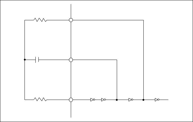
BLOCK DIAGRAM
To LCD panel
|
SEG 1 |
|
SEG 80 |
|
|
SEG-TEST |
|
80-Dot Segment Driver |
|
||
|
|
|
|||
BLANK |
|
|
|
|
|
|
|
|
80 |
|
|
|
|
80-Ch Data Selector |
|
||
VDD |
|
80 |
80 |
|
|
GND |
|
(A) |
(B) |
|
|
80-Bit Data Latch |
80-Bit Data Latch |
|
|||
|
|
||||
LOAD |
|
|
|
|
|
DATA-IN |
|
(A) |
(B) |
DATA-OUT 2 |
|
80-Stage Shift Register |
80-Stage Shift Register |
||||
|
|
||||
CLOCK |
|
|
|
DATA-OUT 1 |
|
|
|
|
|
||
D/S |
|
|
|
|
|
OSC-OUT |
|
|
|
VLC1 |
|
OSC-OUT |
OSC |
1/4 or 1/8 |
1/2 |
VLC2 |
|
OSC-IN |
|
|
Common |
COM-A |
|
|
|
Driver |
|||
EXT/INT |
|
|
|
COM-B |
|
SYNC |
SYNC |
|
|
COM-OUT |
|
Circuit |
|
||||
|
|
|
|||
2/18
¡ Semiconductor |
MSM5265 |
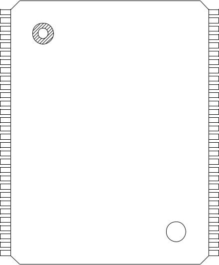
PIN CONFIGURATION (TOP VIEW)
SEG50 |
|
SEG49 |
|
SEG48 |
|
SEG47 |
|
SEG46 |
|
SEG45 |
|
SEG44 |
|
SEG43 |
|
SEG42 |
|
SEG41 |
|
SEG40 |
|
SEG39 |
|
SEG38 |
|
SEG37 |
|
SEG36 |
|
SEG35 |
|
SEG34 |
|
SEG33 |
|
SEG32 |
|
SEG31 |
|
|
|
|
|
|
|
|
|
|
|
|
|
|
|
|
|
|
|
|
|
|
|
|
|
|
|
|
|
|
|
|
|
|
|
|
|
|
|
100 |
|
99 |
|
98 |
|
97 |
|
96 |
|
95 |
|
94 |
|
93 |
|
92 |
|
91 |
|
90 |
|
89 |
|
88 |
|
87 |
|
86 |
|
85 |
|
84 |
|
83 |
|
82 |
|
81 |
SEG51 1
SEG52 2
SEG53 3
SEG54 4
SEG55 5
SEG56 6
SEG57 7
SEG58 8
SEG59 9
SEG60 10
SEG61 11
SEG62 12
SEG63 13
SEG64 14
SEG65 15
SEG66 16
SEG67 17
SEG68 18
SEG69 19
SEG70 20
SEG71 21
SEG72 22
SEG73 23
SEG74 24
SEG75 25
SEG76 26
SEG77 27
SEG78 28
SEG79 29
SEG80 30
31 |
|
32 |
|
33 |
|
34 |
|
35 |
|
36 |
|
37 |
|
38 |
|
39 |
|
40 |
|
41 |
|
42 |
|
43 |
|
44 |
|
45 |
|
46 |
|
47 |
|
48 |
|
49 |
|
50 |
|
|
|
|
|
|
|
|
|
|
|
|
|
|
|
|
|
|
|
|
|
|
|
|
|
|
|
|
|
|
|
|
|
|
|
|
|
|
|
LOAD |
|
CLOCK |
|
DATA-IN |
|
-DATAOUT1 |
|
-DATAOUT2 |
OSC-OUT |
|
OSC-OUT |
|
OSC-IN |
|
EXT/INT |
|
V |
D/S |
|
GND |
|
SEG-TEST |
|
BLANK |
SYNC |
|
COM-OUT |
|
V |
COM-A |
|
COM-B |
|
V |
||||
|
|
|
|
|
|
|
|
|
|
|
|
|
|
|
|
|
|
DD |
|
|
|
|
|
|
|
|
|
|
|
|
LC1 |
|
|
|
|
LC2 |
||
100-Pin Plastic QFP
80 SEG30
79 SEG29
78 SEG28
77 SEG27
76 SEG26
75 SEG25
74 SEG24
73 SEG23
72 SEG22
71 SEG21
70 SEG20
69 SEG19
68 SEG18
67 SEG17
66 SEG16
65 SEG15
64 SEG14
63 SEG13
62 SEG12
61 SEG11
60 SEG10
59 SEG9
58 SEG8
57 SEG7
56 SEG6
55 SEG5
54 SEG4
53 SEG3
52 SEG2
51 SEG1
3/18
¡ Semiconductor |
MSM5265 |
ABSOLUTE MAXIMUM RATINGS
Parameter |
Symbol |
Condition |
Rating |
Unit |
|
|
|
|
|
Supply Voltage |
VDD |
Ta = 25°C |
–0.3 to +6.5 |
V |
Input Voltage |
VI |
Ta = 25°C |
GND–0.3 to VDD +0.3 |
V |
Storage Temperature |
TSTG |
— |
–55 to +150 |
°C |
RECOMMENDED OPERATING CONDITIONS
Parameter |
Symbol |
Condition |
Range |
Unit |
|
|
|
|
|
Supply Voltage |
VDD |
— |
3 to 6 |
V |
Operating Temperature |
Top |
— |
–40 to +85 |
°C |
LCD Driving Voltage |
VLCD |
VDD–VLC2 |
3 to VDD |
V |
• Oscillation circuit
Parameter |
Symbol |
Corresponding pin |
Condition |
Min. |
Typ. |
Max. |
Unit |
|
|
|
|
|
|
|
|
|
|
Oscillator Resistance |
R0 |
OSC-OUT |
— |
56 |
100 |
220 |
kW |
|
Oscillator Capacitance |
C0 |
OSC-OUT |
Film capacitor |
0.001 |
— |
0.047 |
mF |
|
|
|
|
|
|
|
|
|
|
Current Limiting Resistance |
R1 |
OSC-IN |
R1³10 R0 |
0.56 |
1 |
2.2 |
MW |
|
|
|
|
|
|
|
|
|
|
Common Signal Frequency |
fCOM |
COM-A |
— |
25 |
— |
150 |
Hz |
|
COM-B |
||||||||
|
|
|
|
|
|
|
||
|
|
|
|
|
|
|
|
(MSM5265) |
R0 |
OSC-OUT |
C0 |
OSC-OUT |
R1 |
OSC-IN |
4/18
¡ Semiconductor |
MSM5265 |
ELECTRICAL CHARACTERISTICS
DC Characteristics
(VDD = 5.0 V Ta =–40 to +85°C)
Parameter |
Symbol |
Condition |
Min. |
Typ. |
Max. |
Unit |
Applicable pin |
|
|
|
|
|
|
|
|
|
|
"H" Input |
VIH |
— |
|
36 |
— |
VDD |
V |
|
Voltage |
|
|
||||||
|
|
|
|
|
|
|
|
SEG-TEST, BLANK, |
"L" Input |
|
|
|
|
|
|
|
|
VIL |
— |
|
GND |
— |
1.0 |
V |
LOAD, DATA-IN, CLOCK, |
|
Voltage |
|
|||||||
|
|
|
|
|
|
|
D/S, EXT/INT, OSC-IN |
|
|
|
|
|
|
|
|
|
|
Input |
IIL |
VI = 5.0 V/0 V |
|
— |
— |
±1 |
mA |
|
Leakage |
|
|
||||||
Current |
|
|
|
|
|
|
|
|
|
|
|
|
|
|
|
|
|
"H" Output |
|
|
|
|
|
|
|
DATA-OUT1 |
VOH |
IO = –100 mA |
|
4.5 |
— |
— |
V |
DATA-OUT2 |
|
Voltage |
|
|||||||
|
|
|
|
|
|
|
COM-OUT |
|
|
|
|
|
|
|
|
|
|
|
|
|
|
|
|
|
|
|
|
|
IO = –200 mA |
|
4.5 |
— |
— |
V |
OSC-OUT |
|
|
|
OSC-OUT |
|||||
|
|
|
|
|
|
|
|
|
|
|
|
|
|
|
|
|
|
|
|
VLC1 = 2.5 V, VLC2 |
= 0 V |
4.8 |
— |
— |
V |
SEG1-SEG80 |
|
|
IO = –30 mA |
|
|||||
|
|
|
|
|
|
|
|
|
|
|
VLC1 = 2.5 V, VLC2 |
= 0 V |
4.8 |
— |
— |
V |
COM-A |
|
|
IO = –150 mA |
|
COM-B |
||||
|
|
|
|
|
|
|
||
"M" Output |
VOM |
VLC1 = 2.5 V, VLC2 |
= 0 V |
2.3 |
— |
2.7 |
V |
COM-A |
Voltage |
IO = ±150 mA |
|
COM-B |
|||||
|
|
|
|
|
|
|||
"L" Output |
|
IO = 100 mA |
|
|
|
|
|
DATA-OUT1 |
VOL |
|
— |
— |
0.5 |
V |
DATA-OUT2 |
||
Voltage |
|
|||||||
|
|
|
|
|
|
|
COM-OUT |
|
|
|
|
|
|
|
|
|
|
|
|
|
|
|
|
|
|
|
|
|
IO = 200 mA |
|
— |
— |
0.5 |
V |
OSC-OUT |
|
|
|
OSC-OUT |
|||||
|
|
|
|
|
|
|
|
|
|
|
|
|
|
|
|
|
|
|
|
VLC1 = 2.5 V, VLC2 |
= 0 V |
— |
— |
0.2 |
V |
SEG1 - SEG80 |
|
|
IO = 30 mA |
|
|||||
|
|
|
|
|
|
|
|
|
|
|
VLC1 = 2.5 V, VLC2 |
= 0 V |
— |
— |
0.2 |
V |
COM-A |
|
|
IO = 150 mA |
|
COM-B |
||||
|
|
|
|
|
|
|
||
|
|
IO = 250 mA |
|
— |
— |
0.8 |
V |
SYNC |
|
|
|
|
|
|
|
|
|
Output |
|
VO = 5 V |
|
— |
— |
5 |
mA |
SYNC |
Leakage |
ILO |
when internal Tr is off |
||||||
Current |
|
|
|
|
|
|
|
|
|
|
|
|
|
|
|
|
|
Segment |
|
VLC1 = (5+VLC2)/2 |
|
— |
— |
10 |
kW |
SEG1 - SEG80 |
Output |
RSEG |
VLC2 = 0 to 2 V |
|
|||||
Impedance |
|
|
|
|
|
|
|
|
|
|
|
|
|
|
|
|
|
5/18
¡ Semiconductor |
|
|
|
|
|
|
|
|
|
|
|
|
|
|
|
|
|
|
|
|
|
|
|
|
MSM5265 |
|
||
|
|
|
|
|
|
|
|
|
|
|
|
|
|
|
|
|
|
|
|
|
||||||||
Parameter |
|
Symbol |
|
Condition |
|
|
|
|
|
Min. |
|
Typ. |
|
|
Max. |
|
Unit |
|
Applicable Pin |
|
||||||||
|
|
|
|
|
|
|
|
|
|
|
|
|
|
|
|
|
|
|
|
|
|
|
|
|
|
|
||
Common Output |
|
RCOM |
|
VLC1 = (5+VLC2)/2 |
|
|
|
|
|
— |
|
— |
|
1.5 |
|
kW |
|
COM-A |
|
|||||||||
Impedance |
|
|
VLC2 = 0 to 2 V |
|
|
|
|
|
|
|
|
|
COM-B |
|
||||||||||||||
|
|
|
|
|
|
|
|
|
|
|
|
|
|
|
|
|
|
|
|
|
|
|
||||||
Static Supply |
|
IDD1 |
|
Fix all input levels at |
|
|
|
|
|
— |
|
— |
|
100 |
|
mA |
|
|
|
|||||||||
Current |
|
|
either VDD or GND |
|
|
|
|
|
|
|
|
|
|
|
||||||||||||||
|
|
|
|
|
|
|
|
|
|
|
|
|
|
|
|
|
|
|
|
|
|
VDD |
|
|||||
Dynamic Supply |
|
|
|
No load. |
|
|
|
|
|
|
|
|
|
|
|
|
|
|
|
|
|
|
|
|
|
|
||
|
|
|
|
|
|
|
|
|
|
|
|
|
|
|
|
|
|
|
|
|
|
|
|
|
|
|||
Current |
|
IDD2 |
|
R0 = 100 kW, |
|
|
|
|
|
— |
0.12 |
|
0.5 |
|
mA |
|
|
|
||||||||||
|
|
|
|
C0 = 0.01 mF, R1 = 1 MW |
|
|
|
|
|
|
|
|
|
|
|
|
|
|
|
|
|
|||||||
Switching Characteristics |
|
|
|
|
|
|
|
|
|
|
(VDD = 3.0 to 6.0 V Ta = –40 to +85°C) |
|
||||||||||||||||
|
|
|
|
|
|
|
|
|
|
|
|
|
|
|
|
|
||||||||||||
Parameter |
|
Symbol |
|
|
Condition |
|
|
|
Min. |
|
|
Max. |
|
Unit |
|
Applicable Pin |
|
|||||||||||
|
|
|
|
|
|
|
|
|
|
|
|
|
|
|
|
|
|
|
|
|||||||||
Clock Frequency |
|
|
ff |
|
|
|
— |
|
|
|
— |
|
1 |
|
|
MHz |
|
|
|
|||||||||
Clock Pulse "H" Time |
|
|
ffH |
|
|
|
— |
|
|
|
0.3 |
|
|
|
— |
|
|
|
ms |
|
CLOCK |
|
||||||
Clock Pulse "L" Time |
|
|
ffL |
|
|
|
— |
|
|
|
0.5 |
|
|
|
— |
|
|
|
ms |
|
|
|
||||||
Data Setup Time |
|
|
fD–f |
|
|
|
— |
|
|
|
0.1 |
|
|
|
— |
|
|
|
ms |
|
DATA-IN |
|
||||||
Data Hold Time |
|
|
ff–D |
|
|
|
— |
|
|
|
0.1 |
|
|
|
— |
|
|
|
ms |
|
CLOCK |
|
||||||
"H"‚ "L" Propagation |
|
|
tPHL |
|
Load capacitance of |
|
|
|
|
|
|
|
|
|
|
|
|
DATA-OUT1 |
|
|||||||||
|
|
|
DATA-OUT1, DATA-OUT2: |
|
— |
|
0.8 |
|
|
|
ms |
|
DATA-OUT2 |
|
||||||||||||||
Delay Time |
|
|
tPLH |
|
|
|
|
|
|
|
|
|||||||||||||||||
|
|
|
|
15 pF |
|
|
|
|
|
|
|
|
|
|
|
|
|
|
CLOCK |
|
||||||||
|
|
|
|
|
|
|
|
|
|
|
|
|
|
|
|
|
|
|
|
|
|
|||||||
|
|
|
|
|
|
|
|
|
|
|
|
|
|
|
|
|
|
|
|
|
|
|
||||||
LOAD Pulse "H" Time |
|
|
tL |
|
|
|
— |
|
|
|
0.2 |
|
|
|
— |
|
|
|
ms |
|
LOAD |
|
||||||
Clock ® LOAD Time |
|
|
tf–L |
|
|
|
— |
|
|
|
0.1 |
|
|
|
— |
|
|
|
ms |
|
CLOCK |
|
||||||
|
|
|
|
|
|
|
|
|
|
|
|
|
|
|
|
|
|
|
|
|
|
|
|
|
|
|
LOAD |
|
|
|
|
|
|
|
|
|
|
|
|
|
|
|
|
|
|
|
|
|
|||||||||
OSC-IN Input Frequency |
|
fOSC |
|
|
|
— |
|
|
|
— |
|
5 |
|
|
|
kHz |
|
OSC-IN |
|
|||||||||
|
|
|
|
|
|
|
|
|
|
|
|
|
|
|
|
|
|
|
|
|
|
|
||||||
SYNC Pulse "L" Time |
|
|
ts |
|
|
|
— |
|
|
|
0.2 |
|
|
|
— |
|
|
|
ms |
|
SYNC |
|
||||||
|
|
|
|
|
|
|
|
|
|
|
|
|
|
|
|
|
|
|
|
|
|
|
|
|
|
|
|
|
|
|
|
|
|
|
|
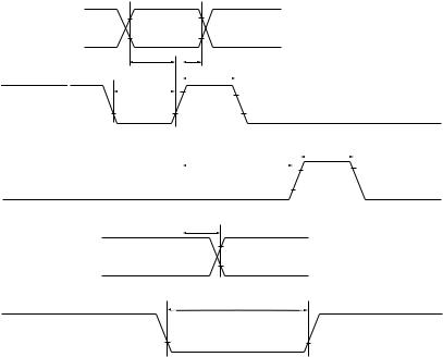
VH |
|
|
|
VH |
|
|
|
|
|
|
|
|
|
|
|
|
|
|
|
|
|
DATA-IN |
|
|
|
|
|
VL |
|
|
|
VL |
|
|
|
|
|
|
|
|
|
|
|
|
|
|
|
|
||
|
|
|
|
|
|
|
tD-f |
|
|
|
tf-D |
tfH |
|
|
|
|
|
|
|
|
|
|
||||||
|
|
|
|
|
|
|
|
|
|
|
|
|
|
|
|
|
|
|||||||||||
CLOCK |
|
|
|
|
|
tfL |
|
|
|
|
|
|
|
|
|
|
|
|
|
|
|
|
|
|
|
|
|
|
|
|
|
|
|
|
|
|
VH |
|
VH |
|
|
|
|
|
|
|
|
|
|
||||||||
|
|
|
|
|
|
|
|
|
|
|
|
|
|
|
|
|
|
|
|
|
|
|||||||
|
|
|
|
|
|
VL |
VL |
|
|
|
|
|
VL |
|
|
tL |
|
|
|
|
|
|
|
|||||
|
|
|
|
|
|
|
|
|
|
|
|
|
|
|
|
|
|
|
|
|||||||||
|
|
|
|
|
|
|
|
|
|
|
|
|
tf-L |
|
|
|
|
|
|
|
|
|
||||||
|
|
|
|
|
|
|
|
|
|
|
|
|
|
|
|
|
|
|
|
|
|
|||||||
LOAD |
|
|
|
|
|
|
|
|
|
|
|
|
|
VH |
|
|
|
VH |
|
|
|
|||||||
|
|
|
|
|
|
|
|
|
|
|
|
|
|
|
|
|
|
|
|
|
|
|
|
|
||||
|
|
|
|
|
|
|
|
|
|
|
|
|
|
|
|
|
|
|
|
|
|
|
||||||
|
|
|
|
|
|
|
|
|
|
|
|
|
|
|
|
|
|
VL |
|
|
|
|
|
|
|
|||
|
|
|
|
|
|
|
|
|
|
|
|
|
|
|
|
|
|
|
|
|
|
|
|
|
|
|
||
|
|
|
|
|
|
|
|
|
|
|
tPHL |
|
|
|
|
|
|
|
|
|
|
|
|
|
|
|||
|
|
|
|
|
|
|
|
|
|
|
|
|
|
|
|
|
|
|
|
|
|
|
|
|
||||
DATA-OUT1 |
|
|
|
|
|
|
|
|
|
tPLH |
|
|
|
|
|
|
|
|
|
|
|
|
|
|
||||
|
|
|
|
|
|
|
|
|
|
|
VH |
|
|
|
|
|
|
|
|
|
|
|
|
|
|
|||
|
|
|
|
|
|
|
|
|
|
|
|
|
|
|
|
|
|
|
|
|
|
|
|
|
|
|
||
DATA-OUT 2 |
|
|
|
|
|
|
|
|
|
|
|
VL |
|
|
|
|
|
|
|
|
|
|
|
|
|
|
||
|
|
|
|
|
|
|
|
|
|
|
|
|
|
|
|
|
|
|
|
|
|
|
|
|
|
|
||
SYNC |
|
|
|
|
|
|
|
|
|
|
|
ts |
|
|
|
|
|
|
|
|
|
|
|
|
|
|
||
|
|
|
|
|
|
|
|
|
|
|
|
|
|
|
|
|
|
|
|
|
|
|
|
|
|
|
||
|
|
|
|
|
|
|
|
VL |
|
|
|
|
|
|
|
|
VL |
|
|
|
|
|
|
|
||||
|
|
|
|
|
|
|
|
|
|
|
(VH = 0.8 VDD, VL = 0.2 VDD) |
|
|
|
|
|
|
|
||||||||||
|
|
|
|
|
|
|
|
|
|
|
|
|
|
|
|
|
|
|
|
|
|
|
|
|
|
|
|
|
6/18
 Loading...