


OKI MSM51V18165DSL-70TS-K, MSM51V18165DSL-60TS-K, MSM51V18165D-70JS, MSM51V18165D-70TS-K, MSM51V18165DSL-50JS Datasheet
...E2G0133-17-61 |
Preliminary |
|
|
||
¡ Semiconductor |
This version: Mar. 1998 |
|
MSM51V18165D/DSL |
||
Semiconductor |
MSM51V18165D/DSL
1,048,576-Word ´ 16-Bit DYNAMIC RAM : FAST PAGE MODE TYPE WITH EDO
DESCRIPTION
The MSM51V18165D/DSL is a 1,048,576-word ´ 16-bit dynamic RAM fabricated in Oki's silicon- gateCMOStechnology.TheMSM51V18165D/DSLachieveshighintegration,high-speedoperation, andlow-powerconsumptionbecauseOkimanufacturesthedeviceinaquadruple-layerpolysilicon/ double-layer metal CMOS process. The MSM51V18165D/DSL is available in a 42-pin plastic SOJ or 50/44-pin plastic TSOP. The MSM51V18165DSL (the self-refresh version) is specially designed for lower-power applications.
FEATURES
•1,048,576-word ´ 16-bit configuration
•Single 3.3 V power supply, ±0.3 V tolerance
• Input : LVTTL compatible, low input capacitance
•Output : LVTTL compatible, 3-state
•Refresh : 1024 cycles/16 ms, 1024 cycles/128 ms (SL version)
•Fast page mode with EDO, read modify write capability
•CAS before RAS refresh, hidden refresh, RAS-only refresh capability
•CAS before RAS self-refresh capability (SL version)
•Package options:
42-pin 400 mil plastic SOJ |
(SOJ42-P-400-1.27) |
(Product : MSM51V18165D/DSL-xxJS) |
50/44-pin 400 mil plastic TSOP |
(TSOPII50/44-P-400-0.80-K) (Product : MSM51V18165D/DSL-xxTS-K) |
|
|
|
xx indicates speed rank. |
PRODUCT FAMILY
Family |
Access Time (Max.) |
Cycle Time |
Power Dissipation |
|
|||||
|
|
|
|
(Min.) |
|
|
|
||
tRAC |
tAA |
tCAC |
tOEA |
Operating (Max.) |
Standby (Max.) |
|
|||
|
|||||||||
|
|
||||||||
MSM51V18165D/DSL-50 |
50 ns |
25 ns |
13 ns |
13 ns |
84 ns |
450 mW |
1.8 mW/ |
||
|
|
|
|
|
|
|
|||
MSM51V18165D/DSL-60 |
60 ns |
30 ns |
15 ns |
15 ns |
104 ns |
414 mW |
|||
0.72 mW (SL version) |
|||||||||
|
|
|
|
|
|
|
|||
MSM51V18165D/DSL-70 |
70 ns |
35 ns |
20 ns |
20 ns |
124 ns |
378 mW |
|||
|
|
||||||||
|
|
|
|
|
|
|
|
|
|
1/17
¡ Semiconductor |
MSM51V18165D/DSL |
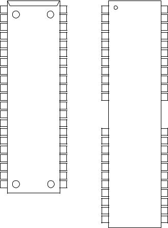
PIN CONFIGURATION (TOP VIEW) |
|
|
|
|
|
||
VCC |
1 |
42 |
VSS |
VCC |
1 |
50 |
VSS |
DQ1 |
2 |
41 |
DQ16 |
DQ1 |
2 |
49 |
DQ16 |
DQ2 |
3 |
40 |
DQ15 |
DQ2 |
3 |
48 |
DQ15 |
DQ3 |
4 |
39 |
DQ14 |
DQ3 |
4 |
47 |
DQ14 |
DQ4 |
5 |
38 |
DQ13 |
DQ4 |
5 |
46 |
DQ13 |
VCC |
6 |
37 |
VSS |
VCC |
6 |
45 |
VSS |
DQ5 |
7 |
36 |
DQ12 |
DQ5 |
7 |
44 |
DQ12 |
DQ6 |
8 |
35 |
DQ11 |
DQ6 |
8 |
43 |
DQ11 |
DQ7 |
9 |
34 |
DQ10 |
DQ7 |
9 |
42 |
DQ10 |
DQ8 10 |
33 |
DQ9 |
DQ8 10 |
41 |
DQ9 |
||
NC 11 |
32 |
NC |
NC 11 |
40 |
NC |
||
NC 12 |
31 |
LCAS |
|
|
|
|
|
WE 13 |
30 |
UCAS |
|
|
|
|
|
RAS 14 |
29 |
OE |
|
|
|
|
|
NC 15 |
28 |
A9 |
NC 15 |
36 |
NC |
||
NC 16 |
27 |
A8 |
NC 16 |
35 |
LCAS |
||
A0 |
17 |
26 |
A7 |
WE 17 |
34 |
UCAS |
|
A1 |
18 |
25 |
A6 |
RAS 18 |
33 |
OE |
|
A2 |
19 |
24 |
A5 |
NC 19 |
32 |
A9 |
|
A3 |
20 |
23 |
A4 |
NC 20 |
31 |
A8 |
|
VCC 21 |
22 |
VSS |
A0 |
21 |
30 |
A7 |
|
|
42-Pin Plastic SOJ |
|
|
A1 |
22 |
29 |
A6 |
|
|
|
A2 |
23 |
28 |
A5 |
|
|
|
|
|
A3 |
24 |
27 |
A4 |
|
|
|
|
VCC 25 |
26 |
VSS |
|
50/44-Pin Plastic TSOP
(K Type)
Pin Name |
Function |
|
|
A0 - A9 |
Address Input |
|
|
RAS |
Row Address Strobe |
LCAS |
Lower Byte Column Address Strobe |
|
|
UCAS |
Upper Byte Column Address Strobe |
DQ1 - DQ16 |
Data Input/Data Output |
|
|
OE |
Output Enable |
|
|
WE |
Write Enable |
VCC |
Power Supply (3.3 V) |
VSS |
Ground (0 V) |
NC |
No Connection |
Note : The same power supply voltage must be provided to every VCC pin, and the same GND voltage level must be provided to every VSS pin.
2/17

¡ Semiconductor MSM51V18165D/DSL
BLOCK DIAGRAM
|
Timing |
|
|
|
WE |
OE |
|
|
|
|
|
RAS |
|
|
|
|
|
|
|
|
|
||
Generator |
|
|
|
|
|
|
|
|
|
||
LCAS |
|
|
|
|
|
|
I/O |
|
|
|
|
|
|
|
|
|
|
Controller |
|
|
Output |
|
|
UCAS |
|
|
|
|
|
|
|
|
8 |
8 |
|
|
|
|
|
|
|
I/O |
|
Buffers |
|||
|
|
|
|
|
|
|
Controller |
|
|
|
DQ1 - DQ8 |
|
|
|
|
|
|
|
|
|
|
|
|
|
10 |
Column |
|
|
|
10 |
Column Decoders |
|
|
Input |
|
|
Address |
|
|
|
|
8 |
8 |
||||
|
|
Buffers |
|
|
|
|
|
|
|
Buffers |
|
|
|
|
|
|
|
|
|
|
|
|
|
|
|
Internal |
|
|
|
Sense Amplifiers 16 |
I/O |
16 |
|
|
|
A0 - A9 |
|
|
Refresh |
|
Selector |
|
|
||||
|
Address |
|
|
|
|
|
|
|
|||
|
|
Counter |
|
Control Clock |
|
|
|
|
|
|
|
|
|
|
|
|
|
|
|
|
|
|
|
|
|
|
|
|
|
|
|
|
8 |
Input |
8 |
|
|
Row |
|
|
|
|
|
|
Buffers |
||
|
|
|
Row |
|
|
|
|
|
|
||
|
|
|
|
|
Memory |
|
|
|
|
||
|
10 |
Address |
10 |
|
|
|
|
|
DQ9 - DQ16 |
||
|
Deco- |
Word |
|
|
|
|
|||||
|
|
Buffers |
|
|
Cells |
|
|
|
|||
|
|
|
ders |
Drivers |
|
|
|
Output |
|
||
|
|
|
|
|
|
|
|
|
8 |
8 |
|
|
|
|
|
|
|
|
|
|
Buffers |
||
|
|
|
|
|
|
|
|
|
|
|
|
VCC
On Chip
VBB Generator
VSS
FUNCTION TABLE
|
|
Input Pin |
|
|
DQ Pin |
Function Mode |
||
|
|
|
|
|
|
|
||
RAS |
LCAS |
UCAS |
WE |
OE |
DQ1 - DQ8 DQ9 - DQ16 |
|||
|
||||||||
|
|
|
|
|
|
|
|
|
H |
* |
* |
* |
* |
High-Z |
High-Z |
Standby |
|
L |
H |
H |
* |
* |
High-Z |
High-Z |
Refresh |
|
L |
L |
H |
H |
L |
DOUT |
High-Z |
Lower Byte Read |
|
L |
H |
L |
H |
L |
High-Z |
DOUT |
Upper Byte Read |
|
L |
L |
L |
H |
L |
DOUT |
DOUT |
Word Read |
|
L |
L |
H |
L |
H |
DIN |
Don't Care |
Lower Byte Write |
|
L |
H |
L |
L |
H |
Don't Care |
DIN |
Upper Byte Write |
|
L |
L |
L |
L |
H |
DIN |
DIN |
Word Write |
|
L |
L |
L |
H |
H |
High-Z |
High-Z |
— |
|
*: "H" or "L"
3/17

¡ Semiconductor MSM51V18165D/DSL
ELECTRICAL CHARACTERISTICS
Absolute Maximum Ratings
|
Parameter |
Symbol |
|
Rating |
|
Unit |
|
|
Voltage on Any Pin Relative to VSS |
VT |
|
–0.5 to 4.6 |
|
V |
|
|
Short Circuit Output Current |
IOS |
|
50 |
|
mA |
|
|
Power Dissipation |
PD* |
|
1 |
|
W |
|
|
Operating Temperature |
Topr |
|
0 to 70 |
|
°C |
|
|
Storage Temperature |
Tstg |
|
–55 to 150 |
|
°C |
|
|
|
*: Ta = 25°C |
|
|
|
|
|
Recommended Operating Conditions |
|
|
|
(Ta = 0°C to 70°C) |
|||
|
|
|
|
|
|
||
|
|
|
|
|
|
|
|
|
Parameter |
Symbol |
Min. |
Typ. |
Max. |
Unit |
|
|
|
|
|
|
|
|
|
|
Power Supply Voltage |
VCC |
3.0 |
3.3 |
3.6 |
V |
|
|
VSS |
0 |
0 |
0 |
V |
||
|
|
||||||
|
Input High Voltage |
VIH |
2.0 |
— |
VCC + 0.3 |
V |
|
|
Input Low Voltage |
VIL |
–0.3 |
— |
0.8 |
V |
|
Capacitance |
|
|
(VCC = 3.3 V ±0.3 V, Ta = 25°C, f = 1 MHz) |
||||
|
|
|
|
||||
|
Parameter |
Symbol |
Typ. |
|
|
Max. |
Unit |
|
Input Capacitance (A0 - A9) |
CIN1 |
— |
|
|
5 |
pF |
|
Input Capacitance |
CIN2 |
— |
|
|
7 |
pF |
|
(RAS, LCAS, UCAS, WE, OE) |
|
|
||||
|
|
|
|
|
|
|
|
|
|
|
|
|
|
|
|
|
Output Capacitance (DQ1 - DQ16) |
CI/O |
— |
|
|
7 |
pF |
4/17

¡ Semiconductor |
|
|
|
|
|
|
MSM51V18165D/DSL |
||||
DC Characteristics |
|
|
|
|
|
(VCC = 3.3 V ±0.3 V, Ta = 0°C to 70°C) |
|||||
|
|
|
|
|
|
||||||
|
|
|
MSM51V18165MSM51V18165MSM51V18165 |
|
|
||||||
Parameter |
Symbol |
Condition |
D/DSL-50 |
D/DSL-60 |
D/DSL-70 |
Unit |
Note |
||||
|
|
|
|
|
|
|
|
|
|
||
|
|
|
Min. |
Max. Min. |
Max. Min. |
Max. |
|
|
|||
|
|
|
|
|
|
|
|
|
|
|
|
Output High Voltage |
VOH |
IOH = –2.0 mA |
2.4 |
VCC |
2.4 |
|
VCC |
2.4 |
VCC |
V |
|
Output Low Voltage |
VOL |
IOL = 2.0 mA |
0 |
0.4 |
0 |
|
0.4 |
0 |
0.4 |
V |
|
|
|
0 V £ VI £ VCC + 0.3 V; |
|
|
|
|
|
|
|
|
|
Input Leakage Current |
ILI |
All other pins not |
–10 |
10 |
–10 |
|
10 |
–10 |
10 |
mA |
|
|
|
under test = 0 V |
|
|
|
|
|
|
|
|
|
|
|
|
|
|
|
|
|
|
|
|
|
Output Leakage Current |
ILO |
DQ disable |
–10 |
10 |
–10 |
|
10 |
–10 |
10 |
mA |
|
0 V £ VO £ VCC |
|
|
|||||||||
|
|
|
|
|
|
|
|
|
|
|
|
Average Power |
|
RAS, CAS cycling, |
|
|
|
|
|
|
|
|
|
Supply Current |
ICC1 |
— |
125 |
— |
|
115 |
— |
105 |
mA |
1, 2 |
|
tRC = Min. |
|
||||||||||
(Operating) |
|
|
|
|
|
|
|
|
|
|
|
Power Supply |
|
RAS, CAS = VIH |
— |
2 |
— |
|
2 |
— |
2 |
mA |
1 |
ICC2 |
RAS, CAS |
— |
0.5 |
— |
|
0.5 |
— |
0.5 |
|||
Current (Standby) |
|
|
|
||||||||
|
³ VCC –0.2 V |
— |
200 |
— |
|
200 |
— |
200 |
mA |
1, 5 |
|
|
|
|
|||||||||
Average Power |
|
RAS cycling, |
|
|
|
|
|
|
|
|
|
Supply Current |
ICC3 |
CAS = VIH, |
— |
125 |
— |
|
115 |
— |
105 |
mA |
1, 2 |
(RAS-only Refresh) |
|
tRC = Min. |
|
|
|
|
|
|
|
|
|
Power Supply |
|
RAS = VIH, |
|
|
|
|
|
|
|
|
|
ICC5 |
CAS = VIL, |
— |
5 |
— |
|
5 |
— |
5 |
mA |
1 |
|
Current (Standby) |
|
||||||||||
|
DQ = enable |
|
|
|
|
|
|
|
|
|
|
|
|
|
|
|
|
|
|
|
|
|
|
Average Power |
|
RAS cycling, |
|
|
|
|
|
|
|
|
|
Supply Current |
ICC6 |
— |
125 |
— |
|
115 |
— |
105 |
mA |
1, 2 |
|
CAS before RAS |
|
||||||||||
(CAS before RAS Refresh) |
|
|
|
|
|
|
|
|
|
|
|
|
|
|
|
|
|
|
|
|
|
|
|
|
|
|
|
|
|
|
|
|
|
|
|
Average Power |
|
RAS = VIL, |
|
|
|
|
|
|
|
|
|
Supply Current |
ICC7 |
CAS cycling, |
— |
125 |
— |
|
115 |
— |
105 |
mA |
1, 3 |
(Fast Page Mode) |
|
tHPC = Min. |
|
|
|
|
|
|
|
|
|
Average Power |
|
tRC = 125 ms, |
|
|
|
|
|
|
|
|
1, 4, |
Supply Current |
ICC10 |
CAS before RAS, |
— |
300 |
— |
|
300 |
— |
300 |
mA |
|
|
5 |
||||||||||
(Battery Backup) |
|
tRAS £ 1 ms |
|
|
|
|
|
|
|
|
|
|
|
|
|
|
|
|
|
|
|
||
Average Power |
|
|
|
|
|
|
|
|
|
|
|
Supply Current |
ICCS |
RAS £ 0.2 V, |
— |
300 |
— |
|
300 |
— |
300 |
mA |
1, 5 |
(CAS before RAS |
CAS £ 0.2 V |
|
|||||||||
|
|
|
|
|
|
|
|
|
|
||
Self-Refresh) |
|
|
|
|
|
|
|
|
|
|
|
|
|
|
|
|
|
|
|
|
|
|
|
Notes : 1. ICC Max. is specified as ICC for output open condition.
2.The address can be changed once or less while RAS = VIL.
3.The address can be changed once or less while CAS = VIH.
4.VCC – 0.2 V £ VIH £ VCC + 0.3 V, –0.3 V £ VIL £ 0.2 V.
5.SL version.
5/17

¡ Semiconductor |
|
|
|
|
|
MSM51V18165D/DSL |
||||||
|
AC Characteristics (1/2) |
|
|
|
|
|
|
|
|
|
|
|
|
|
|
|
(VCC = 3.3 V ±0.3 V, Ta = 0°C to 70°C) |
Note 1, 2, 3 |
|||||||
|
|
|
MSM51V18165MSM51V18165MSM51V18165 |
|
|
|
|
|||||
|
Parameter |
Symbol |
D/DSL-50 |
D/DSL-60 |
D/DSL-70 |
|
Unit |
Note |
||||
|
|
|
|
|
|
|
|
|
|
|
|
|
|
|
|
Min. |
Max. Min. |
Max. Min. |
Max. |
|
|
|
|
||
Random Read or Write Cycle Time |
tRC |
84 |
— |
104 |
— |
124 |
— |
|
ns |
|
|
|
Read Modify Write Cycle Time |
tRWC |
110 |
— |
135 |
— |
160 |
— |
|
ns |
|
|
|
Fast Page Mode Cycle Time |
tHPC |
20 |
— |
25 |
— |
30 |
— |
|
ns |
|
|
|
Fast Page Mode Read Modify Write |
tHPRWC |
58 |
— |
68 |
— |
78 |
— |
|
ns |
|
|
|
Cycle Time |
|
|
|
|||||||||
|
|
|
|
|
|
|
|
|
|
|
||
Access Time from RAS |
tRAC |
— |
50 |
— |
60 |
— |
70 |
|
ns |
4, 5, 6 |
|
|
Access Time from CAS |
tCAC |
— |
13 |
— |
15 |
— |
20 |
|
ns |
4, 5 |
|
|
Access Time from Column Address |
tAA |
— |
25 |
— |
30 |
— |
35 |
|
ns |
4, 6 |
|
|
Access Time from CAS Precharge |
tCPA |
— |
30 |
— |
35 |
— |
40 |
|
ns |
4, 13 |
|
|
Access Time from OE |
tOEA |
— |
13 |
— |
15 |
— |
20 |
|
ns |
4 |
|
|
Output Low Impedance Time from CAS |
tCLZ |
0 |
— |
0 |
— |
0 |
— |
|
ns |
4 |
|
|
Data Output Hold After CAS Low |
tDOH |
5 |
— |
5 |
— |
5 |
— |
|
ns |
|
|
|
CAS to Data Output Buffer Turn-off Delay Time |
tCEZ |
0 |
13 |
0 |
15 |
0 |
20 |
|
ns |
7, 8 |
|
|
RAS to Data Output Buffer Turn-off Delay Time |
tREZ |
0 |
13 |
0 |
15 |
0 |
20 |
|
ns |
7, 8 |
|
|
OE to Data Output Buffer Turn-off Delay Time |
tOEZ |
0 |
13 |
0 |
15 |
0 |
20 |
|
ns |
7 |
|
|
WE to Data Output Buffer Turn-off Delay Time |
tWEZ |
0 |
13 |
0 |
15 |
0 |
20 |
|
ns |
7 |
|
|
Transition Time |
tT |
1 |
50 |
1 |
50 |
1 |
50 |
|
ns |
3 |
|
|
Refresh Period |
tREF |
— |
16 |
— |
16 |
— |
16 |
|
ms |
|
|
|
Refresh Period (SL version) |
tREF |
— |
128 |
— |
128 |
— |
128 |
|
ms |
16 |
|
|
RAS Precharge Time |
tRP |
30 |
— |
40 |
— |
50 |
— |
|
ns |
|
|
|
RAS Pulse Width |
tRAS |
50 |
10,000 |
60 |
10,000 |
70 |
10,000 |
|
ns |
|
|
|
RAS Pulse Width (Fast Page Mode with EDO) |
tRASP |
50 |
100,000 |
60 |
100,000 |
70 |
100,000 |
|
ns |
|
|
|
RAS Hold Time |
tRSH |
7 |
— |
10 |
— |
13 |
— |
|
ns |
|
|
|
RAS Hold Time referenced to OE |
tROH |
7 |
— |
10 |
— |
13 |
— |
|
ns |
|
|
|
CAS Precharge Time (Fast Page Mode with EDO) |
tCP |
7 |
— |
10 |
— |
10 |
— |
|
ns |
15 |
|
|
CAS Pulse Width |
tCAS |
7 |
10,000 |
10 |
10,000 |
13 |
10,000 |
|
ns |
|
|
|
CAS Hold Time |
tCSH |
35 |
— |
40 |
— |
45 |
— |
|
ns |
|
|
|
CAS to RAS Precharge Time |
tCRP |
5 |
— |
5 |
— |
5 |
— |
|
ns |
13 |
|
|
RAS Hold Time from CAS Precharge |
tRHCP |
30 |
— |
35 |
— |
40 |
— |
|
ns |
13 |
|
|
OE Hold Time from CAS (DQ Disable) |
tCHO |
5 |
— |
5 |
— |
5 |
— |
|
ns |
|
|
|
RAS to CAS Delay Time |
tRCD |
11 |
37 |
14 |
45 |
14 |
50 |
|
ns |
5 |
|
|
RAS to Column Address Delay Time |
tRAD |
9 |
25 |
12 |
30 |
12 |
35 |
|
ns |
6 |
|
|
Row Address Set-up Time |
tASR |
0 |
— |
0 |
— |
0 |
— |
|
ns |
|
|
|
Row Address Hold Time |
tRAH |
7 |
— |
10 |
— |
10 |
— |
|
ns |
|
|
|
Column Address Set-up Time |
tASC |
0 |
— |
0 |
— |
0 |
— |
|
ns |
12 |
|
|
Column Address Hold Time |
tCAH |
7 |
— |
10 |
— |
13 |
— |
|
ns |
12 |
|
|
Column Address to RAS Lead Time |
tRAL |
25 |
— |
30 |
— |
35 |
— |
|
ns |
|
|
|
6/17
 Loading...