


OKI MSM83C154S-xxxTS-K, MSM83C154S-xxxJS, MSM80C154STS-K, MSM80C154SJS, MSM83C154S-xxxRS Datasheet
...E2E1023-27-Y3
This version: Jan. 1998
Semiconductor MSM80C154S/83C154S
¡ Semiconductor
Previous version: Nov. 1996
MSM80C154S/83C154S
CMOS 8-bit Microcontroller
GENERAL DESCRIPTION
The MSM80C154S/MSM83C154S, designed for the high speed version of the existing MSM80C154/MSM83C154, is a higher performance 8-bit microcontroller providing low-power consumption.
The MSM80C154S/MSM83C154S covers the functions and operating range of the existing MSM80C154/83C154/80C51F/80C31F.
The MSM80C154S is identical to the MSM83C154S except it does not contain the internal program memory (ROM).
FEATURES
• Operating range |
|
Operating frequency |
: 0 to 3 MHz (Vcc=2.2 to 6.0 V) |
|
0 to 12 MHz (Vcc=3.0 to 6.0 V) |
|
0 to 24 MHz (Vcc=4.5 to 6.0 V) |
Operating voltage |
: 2.2 to 6.0 V |
Operating temperature |
: –40 to +85°C (Operation at +125°C conforms to |
|
the other specification.) |
•Fully static circuit
•Upward compatible with the MSM80C51F/80C31F
• On-chip program memory |
: |
16K words x 8 bits ROM (MSM83C154S only) |
• On-chip data memory |
: |
256 words x 8 bits RAM |
• External program memory address space : |
64K bytes ROM (Max) |
|
• External data memory address space |
: |
64K bytes RAM |
• I/O ports |
: |
4 ports x 8 bits |
(Port 1, 2, 3, impedance programmable) |
: |
32 |
• 16-bit timer/counters |
: |
3 |
• Multifunctional serial port |
: |
I/O Expansion mode |
|
: |
UART mode (featuring error detection) |
•6-source 2-priority level Interrupt and multi-level
Interrupt available by programming IP and IE registers
•Memory-mapped special function registers
•Bit addressable data memory and SFRs
• Minimum instruction cycle |
: 500 ns @ 24 MHz operation |
• Standby functions |
: Power-down mode (oscillator stop) |
|
Activated by software or hardware; providing |
|
ports with floating or active status |
|
The software power-down stet mode is termi- |
|
natedbyinterruptsignalenablingexecutionfrom |
|
the interrupted address. |
1/40
¡ Semiconductor |
|
MSM80C154S/83C154S |
• Package options |
|
|
40-pin plastic DIP (DIP40-P-600-2.54) |
: |
(Product name: MSM80C154SRS/ |
|
|
MSM83C154S-xxxRS) |
44-pin plastic QFP (QFP44-P-910-0.80-2K) : |
(Product name: MSM80C154SGS-2K/ |
|
|
|
MSM83C154S-xxxGS-2K) |
44-pin QFJ (QFJ44-P-S650-1.27) |
: |
(Product name: MSM80C154SJS/ |
|
|
MSM83C154S-xxxJS) |
44-pin TQFP (TQFP44-P-1010-0.80-K) |
: |
(Product name: MSM80C154STS-K/ |
|
|
MSM83C154S-xxxTS-K) |
xxx: indicates the code number
2/40

|
P2.0 |
PORT 2 |
|
|
|
|
|
|
|
|
|
|
(MSM83C154S)DIAGRAMBLOCK |
Semiconductor¡ |
ALE |
TIMING |
|
|
ADDRESSDECODER |
|
DPH |
|
CONTROL |
SIGNAL |
R/W |
SIGNAL |
|||
PCON |
|
|
|
|
||||||||||
|
P2.7 |
|
|
|
|
|
|
|
|
|||||
|
P0.0 |
|
|
|
|
ROM |
|
|
|
|
SPECIAL |
|
|
|
|
|
0 |
|
|
|
|
DPL |
|
PLA |
|
FUNCTION |
|
|
|
|
|
PORT |
|
|
|
|
|
|
|
|
REGISTER |
|
|
|
|
|
PCHL |
PCLL |
16K WORDS x 8BITS |
|
|
|
|
ADDRESS |
|
|
|||
|
P0.7 |
|
|
|
|
DECODER |
|
|
||||||
|
|
|
|
|
|
|
|
|
|
|
|
|||
XTAL1 |
|
|
PCH |
PCL |
|
SENSE AMP |
SP |
|
IR |
|
AIR |
|
|
|
XTAL2 |
|
|
|
|
|
|
|
|
|
|
|
|
|
|
|
|
|
|
|
|
|
|
|
|
|
|
|
|
|
|
andOSC |
IOCON |
|
|
|
|
|
|
|
|
|
C-ROM |
|
|
PSEN |
|
|
|
|
|
|
|
|
|
|
|
|
||
|
|
|
|
|
|
|
|
|
|
|
|
|
|
|
EA |
|
|
|
|
|
|
|
|
|
|
|
|
|
|
RESET |
|
|
T2CON |
TL2 |
TH2 |
R/W AMP |
|
|
ACC |
TR2 |
TR1 |
|
|
|
|
|
|
|
|
|
|
|
|
|
|
|
|
|
|
P1.0 |
|
|
|
|
|
RAM |
|
RAMDP |
|
|
|
|
|
|
1 |
|
|
RCAP2L |
RCAP2H |
256 WORDS |
|
PSW |
|
|
BR |
|
|
||
|
|
TIMER/ |
x 8BITS |
|
|
|
|
|
|
|||||
|
PORT 3 PORT |
|
|
|
ALU |
|
|
|
||||||
|
|
|
|
|
|
|
|
|
|
|
|
|||
|
|
COUNTER 2 |
|
|
|
|
|
|
|
|
|
|
||
P1.7 |
|
|
|
|
|
|
|
|
|
|
|
MSM80C154S/83C154S |
||
|
|
|
|
|
|
|
|
|
|
|
|
|||
3/40 |
|
|
|
|
|
|
|
|
|
|
|
|
||
P3.0 |
|
|
|
|
|
|
|
|
|
|
|
|
|
|
|
|
TH1 |
TL1 |
TH0 |
TL0 |
TMOD |
TCON |
IE |
IP |
SBUF(T) |
SBUF(R) |
SCON |
|
|
P3.7 |
|
|
|
TIMER/COUNTER 0 & 1 |
|
INTERRUPT |
|
SERIAL IO |
|
|
|
|||
|
|
|
|
|
|
|
|
|
||||||

¡ Semiconductor |
MSM80C154S/83C154S |
PIN CONFIGURATION (TOP VIEW)
|
|
|
|
|
P1.0/T2 |
1 |
|
40 |
VCC |
P1.1/T2EX |
|
|
|
P0.0 |
2 |
39 |
|||
P1.2 |
|
|
|
P0.1 |
3 |
38 |
|||
P1.3 |
|
|
|
P0.2 |
4 |
37 |
|||
P1.4 |
|
|
|
P0.3 |
5 |
36 |
|||
|
|
|
|
P0.4 |
P1.5 |
6 |
|
35 |
|
|
|
|
|
P0.5 |
P1.6 |
7 |
|
34 |
|
|
|
|
|
P0.6 |
P1.7 |
8 |
|
33 |
|
|
|
|
|
P0.7 |
RESET |
9 |
|
32 |
|
|
|
|
|
EA |
P3.0/RXD |
10 |
|
31 |
|
|
|
|
|
ALE |
P3.1/TXD |
11 |
|
30 |
|
P3.2/INT0 |
|
|
|
PSEN |
12 |
|
29 |
||
P3.3/INT1 |
|
|
|
P2.7 |
13 |
|
28 |
||
|
|
|
|
P2.6 |
P3.4/T0 |
14 |
|
27 |
|
|
|
|
|
P2.5 |
P3.5/T1/HPDI |
15 |
|
26 |
|
P3.6/WR |
|
|
|
P2.4 |
16 |
|
25 |
||
P3.7/RD |
|
|
|
P2.3 |
17 |
|
24 |
||
XTAL2 |
|
|
|
P2.2 |
18 |
|
23 |
||
|
|
|
|
P2.1 |
XTAL1 |
19 |
|
22 |
|
|
|
|
|
|
VSS |
20 |
|
21 |
P2.0 |
|
|
|||
|
|
|
|
|
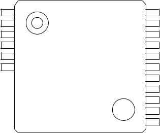
40-Pin Plastic DIP
4/40
¡ Semiconductor |
MSM80C154S/83C154S |
PIN CONFIGURATION (Continued)
|
|
|
P1.4 |
|
P1.3 |
|
P1.2 |
|
P1.1 |
|
P1.0 |
|
NC |
|
V |
|
P0.0 |
|
P0.1 |
|
P0.2 |
|
P0.3 |
|
|
|
|
|
|
|
|
|
|
|
|
|
|
|
|
|
CC |
|
|
|
|
|
|
|
|
|
|
|
|
44 |
|
43 |
|
42 |
|
41 |
|
40 |
|
39 |
|
38 |
|
37 |
|
36 |
|
35 |
|
34 |
|
|
|
P1.5 |
1 |
|
|
|
|
|
|
|
|
|
|
|
|
|
|
|
|
|
|
|
|
|
|
|
P0.4 |
|
|
|
|
|
|
|
|
|
|
|
|
|
|
|
|
|
|
|
|
33 |
|||||
P1.6 |
2 |
|
|
|
|
|
|
|
|
|
|
|
|
|
|
|
|
|
|
|
|
32 |
P0.5 |
||
P1.7 |
3 |
|
|
|
|
|
|
|
|
|
|
|
|
|
|
|
|
|
|
|
|
31 |
P0.6 |
||
RESET |
4 |
|
|
|
|
|
|
|
|
|
|
|
|
|
|
|
|
|
|
|
|
30 |
P0.7 |
||
P3.0/RXD |
5 |
|
|
|
|
|
|
|
|
|
|
|
|
|
|
|
|
|
|
|
|
29 |
EA |
||
NC |
6 |
|
|
|
|
|
|
|
|
|
|
|
|
|
|
|
|
|
|
|
|
28 |
NC |
||
P3.1/TXD |
|
|
|
|
|
|
|
|
|
|
|
|
|
|
|
|
|
|
|
|
|
27 |
ALE |
||
7 |
|
|
|
|
|
|
|
|
|
|
|
|
|
|
|
|
|
|
|
|
|||||
P3.2/INT0 |
|
|
|
|
|
|
|
|
|
|
|
|
|
|
|
|
|
|
|
|
|
26 |
PSEN |
||
8 |
|
|
|
|
|
|
|
|
|
|
|
|
|
|
|
|
|
|
|
|
|||||
P3.3/INT1 |
|
|
|
|
|
|
|
|
|
|
|
|
|
|
|
|
|
|
|
|
|
25 |
P2.7 |
||
9 |
|
|
|
|
|
|
|
|
|
|
|
|
|
|
|
|
|
|
|
|
|||||
P3.4/T0 |
|
|
|
|
|
|
|
|
|
|
|
|
|
|
|
|
|
|
|
|
|
24 |
P2.6 |
||
10 |
|
|
|
|
|
|
|
|
|
|
|
|
|
|
|
|
|
|
|
|
|||||
P3.5/T1/HPDI |
|
|
|
|
|
|
|
|
|
|
|
|
|
|
|
|
|
|
|
|
|
23 |
P2.5 |
||
11 |
|
|
|
|
|
|
|
|
|
|
|
|
|
|
|
|
|
|
|
|
|||||
|
|
|
|
|
|
|
|
|
|
|
|
|
|
||||||||||||
|
|
|
12 |
|
13 |
|
14 |
|
15 |
|
16 |
|
17 |
|
18 |
|
19 |
|
20 |
|
21 |
|
22 |
|
|
|
|
|
|
|
|
|
|
|
|
|
|
|
|
|
|
|
|
|
|
|
|
|
|
|
|
|
|
|
P3.6/WR |
|
P3.7/RD |
|
XTAL2 |
|
XTAL1 |
|
V |
|
V |
|
P2.0 |
|
P2.1 |
|
P2.2 |
|
P2.3 |
|
P2.4 |
|
|
|
|
|
|
|
|
|
|
|
|
|
SS |
|
SS |
|
|
|
|
|
|
|
|
|
|
|
|
NC : No-connection pin
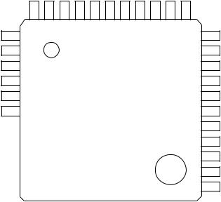
44-Pin Plastic QFP
5/40
¡ Semiconductor |
MSM80C154S/83C154S |
|
|
|
P1.4 |
|
P1.3 |
|
P1.2 |
|
P1.1 |
|
P1.0 |
|
NC |
|
V |
|
P0.0 |
|
P0.1 |
|
P0.2 |
|
P0.3 |
|
|
|
|
|
|
|
|
|
|
|
|
|
|
|
|
|
CC |
|
|
|
|
|
|
|
|
|
|
|
44 |
43 |
42 |
41 |
40 |
39 |
38 |
37 |
36 |
35 |
34 |
|
|
||||||||||||
P1.5 |
1 |
|
|
|
|
|
|
|
|
|
|
|
|
|
|
|
|
|
|
|
|
33 |
P0.4 |
||
P1.6 |
2 |
|
|
|
|
|
|
|
|
|
|
|
|
|
|
|
|
|
|
|
|
32 |
P0.5 |
||
P1.7 |
3 |
|
|
|
|
|
|
|
|
|
|
|
|
|
|
|
|
|
|
|
|
31 |
P0.6 |
||
RESET |
4 |
|
|
|
|
|
|
|
|
|
|
|
|
|
|
|
|
|
|
|
|
30 |
P0.7 |
||
P3.0/RXD |
5 |
|
|
|
|
|
|
|
|
|
|
|
|
|
|
|
|
|
|
|
|
29 |
EA |
||
NC |
6 |
|
|
|
|
|
|
|
|
|
|
|
|
|
|
|
|
|
|
|
|
28 |
NC |
||
P3.1/TXD |
|
|
|
|
|
|
|
|
|
|
|
|
|
|
|
|
|
|
|
|
|
27 |
ALE |
||
7 |
|
|
|
|
|
|
|
|
|
|
|
|
|
|
|
|
|
|
|
|
|||||
P3.2/INT0 |
|
|
|
|
|
|
|
|
|
|
|
|
|
|
|
|
|
|
|
|
|
26 |
PSEN |
||
8 |
|
|
|
|
|
|
|
|
|
|
|
|
|
|
|
|
|
|
|
|
|||||
P3.3/INT1 |
|
|
|
|
|
|
|
|
|
|
|
|
|
|
|
|
|
|
|
|
|
25 |
P2.7 |
||
9 |
|
|
|
|
|
|
|
|
|
|
|
|
|
|
|
|
|
|
|
|
|||||
P3.4/T0 |
|
|
|
|
|
|
|
|
|
|
|
|
|
|
|
|
|
|
|
|
|
24 |
P2.6 |
||
10 |
|
|
|
|
|
|
|
|
|
|
|
|
|
|
|
|
|
|
|
|
|||||
P3.5/T1/HPDI |
|
|
|
|
|
|
|
|
|
|
|
|
|
|
|
|
|
|
|
|
|
23 |
P2.5 |
||
11 |
|
|
|
|
|
|
|
|
|
|
|
|
|
|
|
|
|
|
|
|
|||||
|
|
|
|
|
|
|
|
|
|
|
|
|
|
|
|
|
|
|
|
|
|
|
|
||
|
|
|
12 |
|
13 |
|
14 |
|
15 |
|
16 |
|
17 |
|
18 |
|
19 |
|
20 |
|
21 |
|
22 |
|
|
|
|
|
|
|
|
|
|
|
|
|
|
|
|
|
|
|
|
|
|
|
|
|
|
|
|
|
|
|
P3.6/WR |
|
P3.7/RD |
|
XTAL2 |
|
XTAL1 |
|
V |
|
V |
|
P2.0 |
|
P2.1 |
|
P2.2 |
|
P2.3 |
|
P2.4 |
|
|
|
|
|
|
|
|
|
|
|
|
|
SS |
|
SS |
|
|
|
|
|
|
|
|
|
|
|
|
NC : No-connection pin
44-Pin Plastic TQFP
6/40
¡ Semiconductor |
MSM80C154S/83C154S |
PIN CONFIGURATION (Continued)
P0.4 |
|
P0.5 |
|
P0.6 |
|
P0.7 |
EA |
|
NC |
|
ALE |
PSEN |
|
P2.7 |
|
P2.6 |
|
P2.5 |
||
|
|
|
|
|
|
|
|
|
|
|
|
|
|
|
|
|
|
|
|
|
39 |
|
38 |
|
37 |
|
36 |
|
35 |
|
34 |
|
33 |
|
32 |
|
31 |
|
30 |
|
29 |
P0.3 40
P0.2 41
P0.1 42
P0.0 43
VCC 44
NC 1
P1.0/T2 2
P1.1/T2EX 3
P1.2 4
P1.3 5
P1.4 6
7 |
|
8 |
|
9 |
|
10 |
|
11 |
|
12 |
|
13 |
|
14 |
|
15 |
|
16 |
|
17 |
P1.5 |
|
P1.6 |
|
P1.7 |
|
RESET |
|
P3.0/RXD |
NC |
|
P3.1/TXD |
P3.2/INT0 |
P3.3/INT1 |
|
P3.4/T0 |
|
P3.5/T1/HPDI |
|||
NC : No-connection pin
44-Pin Plastic QFJ
28 P2.4
27 P2.3
26 P2.2
25 P2.1
24 P2.0
23 NC
22 VSS
21 XTAL1
20 XTAL2
19 P3.7/RD
18 P3.6/WR
7/40

¡ Semiconductor |
MSM80C154S/83C154S |
PIN DESCRIPTIONS
Symbol |
Descriptipn |
P0.0 to P0.7 Bidirectional I/O ports. They are also the data/address bus (input/output of data and output of lower 8-bit address when external memory is accessed).
They are open-drain outputs when used as I/O ports, but 3-state outputs when used as data/address bus.
P1.0 to P1.7 P1.0 to P1.7 are quasi-bidirectional I/O ports. They are pulled up internally when used as input |
||
|
ports. Two of them have the following secondary functions: |
|
|
•P1.0 (T2) |
: used as external clock input pins for the timer/counter 2. |
|
•P1.1 (T2EX) |
: used as trigger input for the timer/counter 2 to be reloaded or captured; |
|
|
causing the timer/counter 2 interrupt. |
|
||
P2.0 to P2.7 P2.0 to P2.7 are quasi-bidirectional I/O ports. They also output the higher 8-bit address when |
||
|
an external memory is accessed. They are pulled up internally when used as input ports. |
|
|
||
P3.0 to P3.7 P3.0 to P3.7 are quasi-bidirectional I/O ports. They are pulled up internally when used as input |
||
|
ports. They also have the following secondary functions: |
|
|
•P3.0 (RXD) |
|
|
Serial data input/output in the I/O expansion mode and serial data input in the UART mode when |
|
|
the serial port is used. |
|
|
•3.1 (TXD) |
|
|
Synchronous clock output in the I/O expansion mode and serial data output in the UART mode |
|
|
when the serial port is used. |
|
|
•3.2 (INT0) |
|
|
Used as input pin for the external interrupt 0, and as count-up control pin for the timer/counter 0. |
|
|
•3.3 (INT1) |
|
|
Used as input pin for the external interrupt 1, and as count-up control pin for the timer/counter 1. |
|
|
•3.4 (T0) |
|
|
Used as external clock input pin for the timer/counter 0. |
|
|
•3.5 (T1) |
|
|
Used as external clock input pin for the timer/counter 1 and power-down-mode control input pin. |
|
|
•3.6 (WR) |
|
|
Output of the write-strobe signal when data is written into external data memory. |
|
|
•3.7 (RD) |
|
|
Output of the read-strobe signal when data is read from external data memory. |
|
|
|
|
ALE |
Address latch enable output for latching the lower 8-bit address during external memory access. |
|
|
Two ALE pulses are activated per machine cycle except during external data memory access at |
|
|
which time one ALE pulse is skipped. |
|
|
|
|
PSEN |
Program store enable output which enables the external memory output to the bus during external |
|
|
program memory access. Two PSEN pulses are activated per machine cycle except during |
|
|
external data memory access at which two PSEN pulses are skipped. |
|
|
|
|
EA |
When EA is held at "H" level, the MSM 83C154S executes instructions from internal program |
|
|
memory at address 0000H to 3FFFH, and executes instructions from external program memory |
|
|
above address 3FFFH. |
|
|
When EA is held at "L" level, the MSM80C154S/MSM83C154S executes instructions from external |
|
|
program memory for all addresses. |
|
8/40

¡ Semiconductor MSM80C154S/83C154S
PIN Descriptions (Continued)
Symbol |
Descriptipn |
|
|
RESET |
If this pin remains "H" for at least one machine cycle, the MSM80C154S/MSM83C154S is reset. |
|
Since this pin is pulled down internally, a power-on reset is achieved by simply connecting a |
|
capacitor between VCC and this pin. |
|
|
XTAL1 |
Oscillator inverter input pin. External clock is input through XTAL1 pin. |
|
|
XTAL2 |
Oscillator inverter output pin. |
|
|
VCC |
Power supply pin during both normal operation and standby operations. |
VSS |
GND pin. |
9/40

¡ Semiconductor MSM80C154S/83C154S
REGISTERS
Diagram of Special Function Registers
REGISTER |
|
|
|
BIT ADDRESS |
|
|
|
DIRECT |
|
NAME |
b7 |
b6 |
b5 |
b4 |
b3 |
b2 |
b1 |
b0 |
ADDRESS |
|
|
|
|
|
|
|
|
|
|
IOCON |
FF |
FE |
FD |
FC |
FB |
FA |
F9 |
F8 |
0F8H (248) |
|
|
|
|
|
|
|
|
|
|
B |
F7 |
F6 |
F5 |
F4 |
F3 |
F2 |
F1 |
F0 |
0F0H (240) |
|
|
|
|
|
|
|
|
|
|
ACC |
E7 |
E6 |
E5 |
E4 |
E3 |
E2 |
E1 |
E0 |
0E0H (224) |
|
|
|
|
|
|
|
|
|
|
PSW |
D7 |
D6 |
D5 |
D4 |
D3 |
D2 |
D1 |
D0 |
0D0H (208) |
|
|
|
|
|
|
|
|
|
|
TH2 |
|
|
|
|
|
|
|
|
0CDH (205) |
|
|
|
|
|
|
|
|
|
|
TL2 |
|
|
|
|
|
|
|
|
0CCH (204) |
|
|
|
|
|
|
|
|
|
|
RCAP2H |
|
|
|
|
|
|
|
|
0CBH (203) |
|
|
|
|
|
|
|
|
|
|
RCAP2L |
|
|
|
|
|
|
|
|
0CAH (202) |
|
|
|
|
|
|
|
|
|
|
T2CON |
CF |
CE |
CD |
CC |
CB |
CA |
C9 |
C8 |
0C8H (200) |
|
|
|
|
|
|
|
|
|
|
IP |
BF |
BE |
BD |
BC |
BB |
BA |
B9 |
B8 |
0B8H (184) |
|
|
|
|
|
|
|
|
|
|
P3 |
B7 |
B6 |
B5 |
B4 |
B3 |
B2 |
B1 |
B0 |
0B0H (176) |
|
|
|
|
|
|
|
|
|
|
IE |
AF |
AE |
AD |
AC |
AB |
AA |
A9 |
A8 |
0A8H (168) |
|
|
|
|
|
|
|
|
|
|
P2 |
A7 |
A6 |
A5 |
A4 |
A3 |
A2 |
A1 |
A0 |
0A0H (160) |
|
|
|
|
|
|
|
|
|
|
SBUF |
|
|
|
|
|
|
|
|
99H (153) |
|
|
|
|
|
|
|
|
|
|
SCON |
9F |
9E |
9D |
9C |
9B |
9A |
99 |
98 |
98H (152) |
|
|
|
|
|
|
|
|
|
|
P1 |
97 |
96 |
95 |
94 |
93 |
92 |
91 |
90 |
90H (144) |
|
|
|
|
|
|
|
|
|
|
TH1 |
|
|
|
|
|
|
|
|
8DH (141) |
|
|
|
|
|
|
|
|
|
|
TH0 |
|
|
|
|
|
|
|
|
8CH (140) |
|
|
|
|
|
|
|
|
|
|
TL1 |
|
|
|
|
|
|
|
|
8BH (139) |
|
|
|
|
|
|
|
|
|
|
TL0 |
|
|
|
|
|
|
|
|
8AH (138) |
|
|
|
|
|
|
|
|
|
|
TMOD |
|
|
|
|
|
|
|
|
89H (137) |
|
|
|
|
|
|
|
|
|
|
TCON |
8F |
8E |
8D |
8C |
8B |
8A |
89 |
88 |
88H (136) |
|
|
|
|
|
|
|
|
|
|
PCON |
|
|
|
|
|
|
|
|
87H (135) |
|
|
|
|
|
|
|
|
|
|
DPH |
|
|
|
|
|
|
|
|
83H (131) |
|
|
|
|
|
|
|
|
|
|
DPL |
|
|
|
|
|
|
|
|
82H (130) |
|
|
|
|
|
|
|
|
|
|
SP |
|
|
|
|
|
|
|
|
81H (129) |
P0 |
87 |
86 |
85 |
84 |
83 |
82 |
81 |
80 |
80H (128) |
|
|
|
|
|
|
|
|
|
|
10/40
¡ Semiconductor |
MSM80C154S/83C154S |
Special Function Registers
Timer mode register (TMOD)
NAME |
ADDRESS |
MSB |
|
|
|
|
|
|
|
|
|
LSB |
7 |
6 |
5 |
4 |
|
3 |
|
2 |
1 |
|
0 |
||
|
|
|
|
|
||||||||
|
|
|
|
|
|
|
|
|
|
|
|
|
TMOD |
89H |
GATE |
C/T |
M1 |
M0 |
|
GATE |
|
C/T |
M1 |
|
M0 |
|
|
|
|
|
|
|
|
|
|
|
|
|
BIT LOCATION |
FLAG |
|
|
|
FUNCTION |
|
|
|
|
|||
|
|
|
|
|
|
|
|
|
|
|
|
|
TMOD.0 |
M0 |
M1 |
M0 |
Timer/counter 0 mode setting |
|
|
|
|
||||
|
|
0 |
0 |
8-bit timer/counter with 5-bit prescalar. |
|
|
|
|||||
|
|
0 |
1 |
16-bit timer/counter. |
|
|
|
|
|
|
||
|
|
1 |
0 |
8-bit timer/counter with 8-bit auto reloading. |
|
|||||||
|
|
|
|
Timer/counter 0 separated into TLO (8-bit) timer/counter |
||||||||
TMOD.1 |
M1 |
1 |
1 |
|||||||||
|
|
|
|
and TH0 (8-bit) timer/counter. TF0 is set by TL0 carry, and |
||||||||
|
|
|
|
TF1 is set by TH0 carry. |
|
|
|
|
||||
|
|
|
|
|
|
|
|
|
|
|
|
|
TMOD.2 |
C/T |
Timer/counter 0 count clock designation control bit. |
|
|
|
|
||||||
|
|
XTAL1•2 divided by 12 clocks is the input applied to timer/counter 0 when |
|
|||||||||
|
|
C/T = "0". |
|
|
|
|
|
|
|
|
|
|
|
|
The external clock applied to the T0 pin is the input applied to timer/counter 0 |
||||||||||
|
|
when C/T = "1". |
|
|
|
|
|
|
|
|
|
|
TMOD.3 |
GATE |
When this bit is "0", the TR0 bit of TCON (timer control register) is used to |
|
|||||||||
|
|
control the start and stop of timer/counter 0 counting. |
|
|
|
|
||||||
|
|
If this bit is "1", timer/counter 0 starts counting when both the TR0 bit of TCON |
||||||||||
|
|
and INT0 pin input signal are "1", and stops counting when either is changed |
||||||||||
|
|
to "0". |
|
|
|
|
|
|
|
|
|
|
TMOD.4 |
M0 |
M1 |
M0 |
Timer/counter 1 mode setting |
|
|
|
|
||||
|
|
0 |
0 |
8-bit timer/counter with 5-bit prescalar. |
|
|
|
|||||
|
|
0 |
1 |
16-bit timer/counter |
|
|
|
|
|
|
||
|
|
1 |
0 |
8-bit timer/counter with 8-bit auto reloading. |
|
|||||||
TMOD.5 |
M1 |
|
||||||||||
1 |
1 |
Timer/counter 1 operation stopped. |
|
|
|
|||||||
|
|
|
|
|
||||||||
|
|
|
|
|
|
|
|
|
|
|
|
|
TMOD.6 |
C/T |
Timer/counter 1 count clock designation control bit. |
|
|
|
|
||||||
|
|
XTAL1•2 divided by 12 clocks is the input applied to timer/counter 1 when |
|
|||||||||
|
|
C/T = "0". |
|
|
|
|
|
|
|
|
|
|
|
|
The external clock applied to the T1 pin is the input applied to timer/counter 1 |
||||||||||
|
|
when C/T = "1". |
|
|
|
|
|
|
|
|
|
|
TMOD.7 |
GATE |
When this bit is "0", the TR1 bit of TCON is used to control the start and stop of |
||||||||||
|
|
timer/counter 1 counting. |
|
|
|
|
|
|
|
|
||
|
|
If this bit is "1", timer/counter 1 starts counting when both the TR1 bit of TCON |
||||||||||
|
|
and INT1 pin input signal are "1", and stops counting when either is changed |
||||||||||
|
|
to "0". |
|
|
|
|
|
|
|
|
|
|
11/40
¡ Semiconductor |
|
|
|
|
|
|
|
MSM80C154S/83C154S |
||||||
Power control register (PCON) |
|
|
|
|
|
|
|
|
|
|
|
|
||
|
|
|
|
|
|
|
|
|
|
|
|
|
|
|
NAME |
ADDRESS |
MSB |
|
|
|
|
|
|
|
|
|
|
LSB |
|
7 |
6 |
|
5 |
|
4 |
3 |
|
2 |
1 |
|
0 |
|
||
|
|
|
|
|
|
|
||||||||
|
|
|
|
|
|
|
|
|
|
|
|
|
|
|
PCON |
87H |
SMOD |
HPD |
|
RPD |
|
— |
GF1 |
|
GF0 |
PD |
|
IDL |
|
|
|
|
|
|
|
|
|
|
|
|
|
|
|
|
BIT LOCATION |
FLAG |
|
|
|
|
|
FUNCTION |
|
|
|
|
|
|
|
|
|
|
|
|
|
|
|
|
|
|
||||
PCON.0 |
IDL |
IDLE mode is set when this bit is set to "1". CPU operations are stopped when |
||||||||||||
|
|
IDLE mode is set, but XTAL1•2, timer/counters 0, 1 and 2, the interrupt circuits, |
||||||||||||
|
|
and the serial port remain active. IDLE mode is cancelled when the CPU is reset |
||||||||||||
|
|
or when an interrupt is generated. |
|
|
|
|
|
|
|
|
||||
|
|
|
|
|
|
|
|
|
|
|
||||
PCON.1 |
PD |
PD mode is set when this bit is set to "1". CPU operations and XTAL1•2 are |
||||||||||||
|
|
stopped when PD mode is set. PD mode is cancelled when the CPU is reset or |
||||||||||||
|
|
when an interrupt is generated. |
|
|
|
|
|
|
|
|
||||
|
|
|
|
|
|
|
|
|
|
|
|
|
|
|
PCON.2 |
GF0 |
General purpose bit. |
|
|
|
|
|
|
|
|
|
|
||
|
|
|
|
|
|
|
|
|
|
|
|
|
|
|
PCON.3 |
GF1 |
General purpose bit. |
|
|
|
|
|
|
|
|
|
|
||
|
|
|
|
|
|
|
|
|
|
|
|
|||
PCON.4 |
— |
Reserved bit. The output data is "1", if the bit is read. |
|
|
|
|
||||||||
|
|
|
|
|
|
|
|
|
|
|
||||
PCON.5 |
RPD |
This bit is used to specify cancellation of CPU power down mode (IDLE or PD) by an |
||||||||||||
|
|
interrupt signal. |
|
|
|
|
|
|
|
|
|
|
||
|
|
Power-down mode cannot be cancelled by an interrupt signal if the interrupt is not |
||||||||||||
|
|
enabled by IE (interrupt enable register) when this bit is "0". |
|
|
|
|
||||||||
|
|
If the interrupt flag is set to "1" by an interrupt request signal when this bit is |
||||||||||||
|
|
"1" (even if interrupt is disabled), the program is executed from the next address |
||||||||||||
|
|
of the power-down-mode setting instruction. |
|
|
|
|
|
|
||||||
|
|
The flag is reset to "0" by software. |
|
|
|
|
|
|
|
|||||
|
|
|
|
|
|
|
|
|
|
|
|
|||
PCON.6 |
HPD |
The hard power-down setting mode in enabled when this bit is set to "1". |
|
|
||||||||||
|
|
If the level of the power failure detect signal applied to the HPDI pin (pin 3.5) |
||||||||||||
|
|
is changed from "1" to "0" when this bit is "1", XTAL1•2 oscillation is stopped and |
||||||||||||
|
|
the system is put into hard power down mode. HPD mode is cancelled when the |
||||||||||||
|
|
CPU is reset. |
|
|
|
|
|
|
|
|
|
|
||
PCON.7 |
SMOD |
When the timer/counter 1 carry signal is used as a clock in mode 1, 2 or 3 of |
||||||||||||
|
|
the serial port, this bit has the following functions. |
|
|
|
|
|
|
||||||
|
|
The serial port operation clock is reduced by 1/2 when the bit is "0" for delayed |
||||||||||||
|
|
processing. When the bit is "1", the serial port operation clock is normal |
|
|
||||||||||
|
|
for faster processing. |
|
|
|
|
|
|
|
|
|
|
||
|
|
|
|
|
|
|
|
|
|
|
|
|
|
|
12/40
 Loading...