


MSM6542-2MS-K
OKI MSM6542-2MS-K, MSM6542-2RS, MSM6542-3GS-VK, MSM6542-1MS-K, MSM6542-3RS Datasheet
...
¡ SemiconductorMSM6542-01/02/03
68
DESCRIPTION
The MSM6542 is a perpetual-calendar-based
real time clock with an alarm function which
can read and write data in units of seconds. It
can be connected to various buses and can
function as a peripheral IC of a microcom-
puter.
The clock ranges are seconds, minutes, hours,
days, months, years, and days of the week.
The alarm ranges are seconds, minutes, hours,
days, months, and days of the week.
An event trigger is generated when the time
matches the specified time and an alarm oc-
curs or when the clock counter generates a
carry. The interrupt and pulse outputs are
provided for each of an alarm and a carry.
An interface with a microcomputer is imple-
mented by four data bus pins, four address
bus
¡ Semiconductor
MSM6542-01/02/03
REAL TIME CLOCK WITH PERIODIC AND ALARM OUTPUT
bus pins, three control bus pins, and two chip
select pins. These pins are used to write or
read data from the clock, alarm, and control
registers, or to modify the data.
The MSM6542 has an address latch enable
(ALE) input pin, allowing the data bus and
address bus to be shared. When the ALE
input pin is kept high, the data bus and ad-
dress bus can be exclusively used.
Other functions of the MSM6542 are: a 30-
second adjustment, stop and restart of clock,
data registers as RAM, and data register (RAM)
protection.
The CMOS circuitry used in the MSM6542
affords low power dissipation. The crystal
oscillator operates at 32.768 kHz. Provisions
for backup time keeping are included.
FEATURES
• Real time clock providing seconds, minutes,
hours, days, months, years, and days of
the week.
• Multiple alarm ranges covering seconds,
minutes, hours, days, months, and days of
the week. A desired alarm range can be
selected.
• A periodic interrupt output interval can
be selected over a wide range from 1/1024
seconds up to 10 minutes.
• Interface flexibility allows for connection
to many types of microprocessors.
• Single read-out procedure (Read flag).
• Single power sense circuitry. (Data protect
function).
• Unused registers can be used as RAM.
• 30-second adjustment by software or
hardware (software only for the MSM6542-
1/-2).
• Stop and restart of clock by software or
hardware (software only for the MSM6542-
1/-2).
• 1 Hz output for adjustment and check of
oscillation frequency (MSM6542-3 only).
• User selection of 12 or 24 hour clock mode.
• Address latch enable (ALE) input pin.
• Advanced CMOS circuitry allows low
stand-by voltage and current.
• User standard 32.768 kHz oscillator crys-
tal
• Available in multiple packages
18-pin plastic DIP (for the MSM6542-
1RS/2RS) (DIP18-P-300).
20-pin plastic SOP (for the MSM6542-
1MS-K/2MS-K) (SSOP20-P-250-K).
24-pin plastic DIP (for the MSM6542-
3RS) (DIP24-P-600).
24-pin plastic SOP (for the MSM6542-
3GS-VK) (SOP24-P-430-VK).
• Pin assignment compatibility with the
MSM6242BRS (The MSM6542-3MSK pro-
vides near compatibility.).
¡ Semiconductor MSM6542-01/02/03
69
INTERRUPT
OUT
1
2
3
4
5
6
7
8
9
18
17
16
14
13
12
11
10
ALE
15
E
V
SS
XT
XT
R/W
A
1
A
0
A
2
A
3
D
0
D
1
D
2
D
3
CS
1
CS
0
V
DO
INTERRUPT
OUT
1
2
3
4
5
6
7
8
9
18
17
16
14
13
12
11
10
ALE
15
RD
V
SS
XT
XT
WR
A
1
A
0
A
2
A
3
D
0
D
1
D
2
D
3
CS
1
CS
0
V
DO
124
223
322
421
5
20
6
718
817
916
10 15
11 14
12 13
19
PERIODIC
OUT
ALARM OUT
ALE
30Sec. ADJ
68/80
(E) RD
V
SS
XT
XT
(NC)
STOP/START
1Hz
WR (R/W)
CS
0
A
0
A
1
A
2
A
3
D
1
D
2
D
3
CS
1
1
219
3
20
18
417
516
615
714
813
912
10 11
INTERRUPT OUT
(NC)
ALE
A
0
CS
0
A
1
A
2
A
3
RD
V
SS
XT
XT
(NC)
WR
CS
1
D
0
D
1
D
2
D
3
V
DO
1
219
3
20
18
417
516
615
714
813
912
10 11
INTERRUPT OUT
(NC)
ALE
A
0
CS
0
A
1
A
2
A
3
E
V
SS
XT
XT
(NC)
R/
W
CS
1
D
0
D
1
D
2
D
3
V
DO
12 13
11 14
10 15
916
817
718
619
520
421
322
223
124
PERIODIC OUT
ALARM OUT
ALE
CS
0
A
0
A
1
30Sec. ADJ
A
2
A
3
68/80
(E) RD
V
SS
XT
XT
(NC)
STOP/START
1Hz
CS
1
D
0
D
1
D
2
D
3
WR (R/W)
V
DO
V
DO
D
0
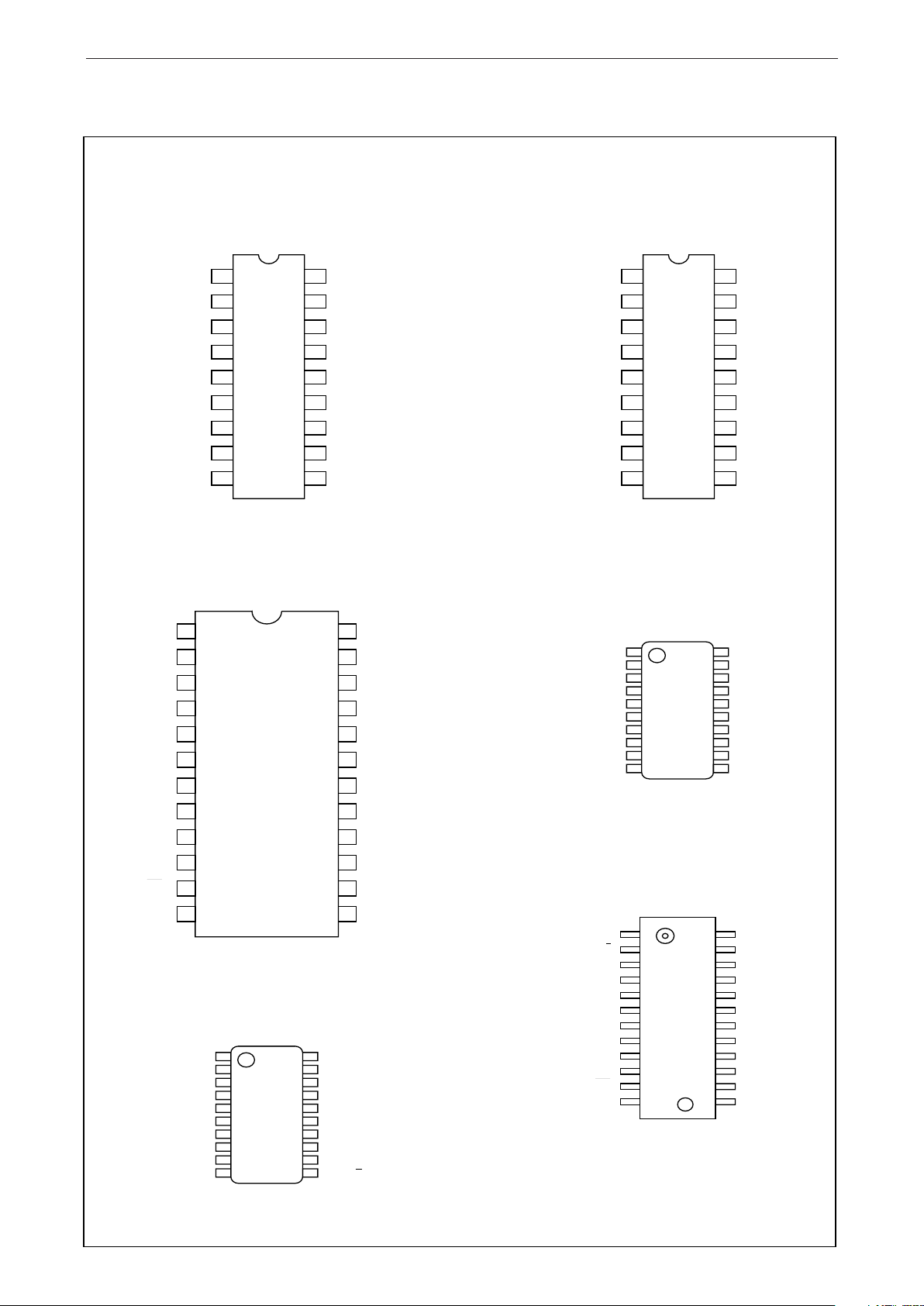
PIN CONFIGURATION
MSM6542-01RS
18-pin plastic DIP (top view)
MSM6542-02RS
18-pin plastic DIP (top view)
MSM6542-03RS
24-pin plastic DIP (top view)
MSM6542-01MS-K
20-pin plastic SOP (top view)
MSM6542-02MS-K
20-pin plastic SOP (top view)
MSM6542-03GS-VK
24-pin plastic SOP (top view)
NC : NO Connected (open)
¡ SemiconductorMSM6542-01/02/03
70
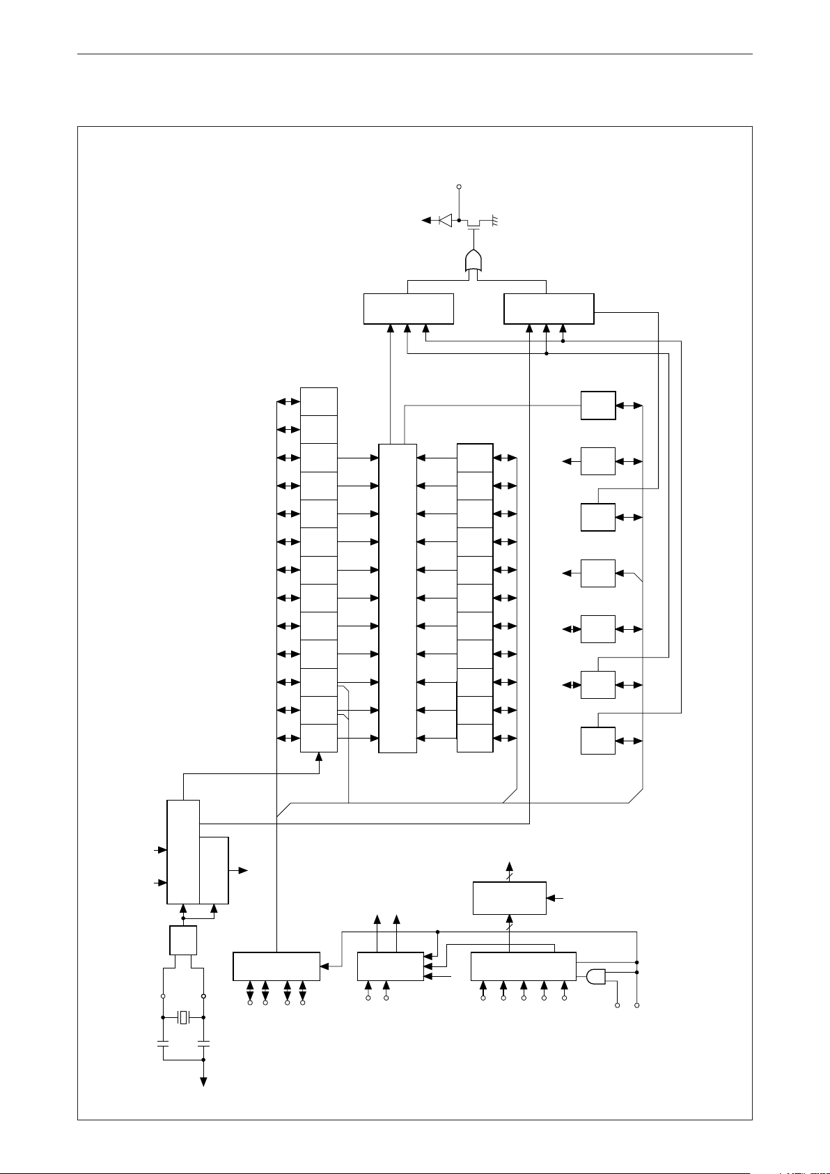
FUNCTIONAL BLOCK DIAGRAM (MSM6542-01, 02)
32.768KHz
XT
XT
OSC
RESET STOP
Less-than-second
counter
Control
counter
D
A
T
A
I.
F.
D
3
D
2
D
1
D
0
A
3
A
2
A
1
A
0
CS
0
WR or R/W
RD or E
(-1) (-2)
R/W
I
F
D.P.
A
D
D
R
E
S
S
I.
F.
D
E
C
O
D
E
R
BANK 1/0
ALE
CS
1
R-S
I
to C
F
A-S
I
to C
E'
R-S
1
R-S
10
R-
MI
10
R-H
1
R-H
10
R-W R-D
1
R-D
10
R-
MO
1
R-
MO
10
R-Y
1
R-Y
10
COMPARATOR
A-S
1
A-S
10
A-H
1
A-H
10
A-W A-D
1
A-D
10
A-
MO
1
A-
MO
10
A-
MI
10
INTERRUPT OUT
C
E'
C
C'
A-EN
ABLE
C
D'
C
F
C
E
C
D
R-
MI
1
A-
MI
1
A
L
A
R
M
O
U
T
P
E
R
I
O
D
I
C
O
U
T
¡ Semiconductor MSM6542-01/02/03
71
32.768KHz
XT
XT
OSC
RESET STOP
1Hz
Less-than-second
counter
Control
counter
D
A
T
A
I.
F.
R/W
I
F
D.P.
A
D
D
R
E
S
S
I.
F.
D
E
C
O
D
E
R
BANK 1/0
D
3
D
2
D
1
D
0
A
3
A
2
A
1
A
0
CS
0
R/W or WR
E or RD
68/80
ALE
CS
1
30sec. ADJ
STOP/START
R-S
I
to C
F
A-S
I
to C
E'
R-S
1
R-S
10
R-
MI
10
R-H
1
R-H
10
R-W R-D
1
R-D
10
R-
MO
1
R-
MO
10
R-Y
1
R-Y
10
COMPARATOR
A-S
1
A-S
10
A-H
1
A-H
10
A-W A-D
1
A-D
10
A-
MO
1
A-
MO
10
A-
MI
10
P
E
R
I
O
D
I
C
O
U
T
C
E'
C
C'
A-EN
ABLE
C
D'
C
F
C
E
C
D
ALARM OUT
PERIODIC OUT
R-
MI
1
A-
MI
1
A
L
A
R
M
O
U
T
FUNCTIONAL BLOCK DIAGRAM (MSM6542-03)
¡ SemiconductorMSM6542-01/02/03
72
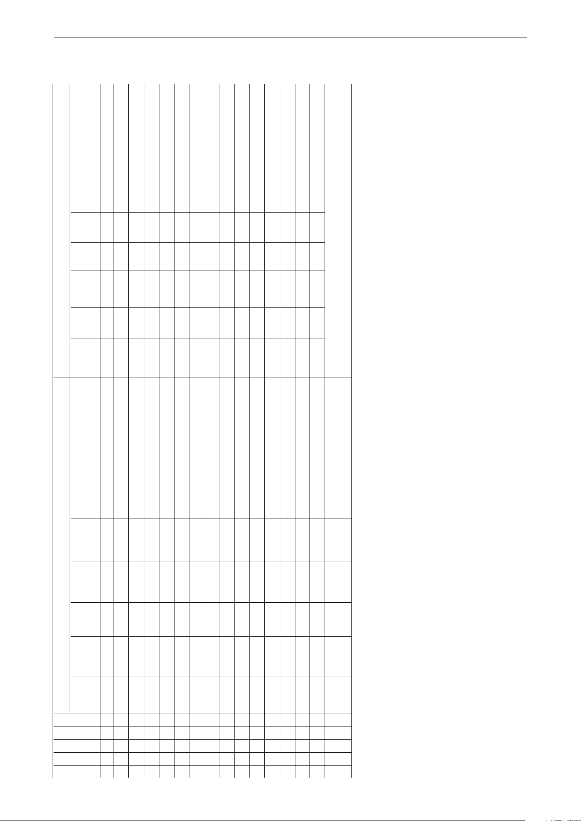
REGISTER TABLE
A
d
d
r
e
s
s
A
3
A
2
A
1
A
0
Register
symbol
D
3
D
2
D
1
D
0
Register name
BANK 0 BANK 1
0
1
2
3
4
5
6
7
8
9
A
B
C
D
E
F
0
0
0
0
0
0
0
0
1
1
1
1
1
1
1
1
0
0
0
0
1
1
1
1
0
0
0
0
1
1
1
1
0
0
1
1
0
0
1
1
0
0
1
1
0
0
1
1
0
1
0
1
0
1
0
1
0
1
0
1
0
1
0
1
R-S
1
R-S
10
R-MI
1
R-MI
10
R-H
1
R-H
10
R-D
1
R-D
10
R-MO
1
R-MO
10
R-Y
1
R-Y
10
R-W
C
D
C
E
C
F
r-s
8
–
r-mi
8
–
r-h
8
–
r-d
8
*
r-mo
8
*
r-y
8
r-y
80
–
IT/PLS
2
IRQ FLAG
0
BANKI/0
r-s
4
r-s
40
r-mi
4
r-mi
40
r-h
4
r-pm/am
r-d
4
*
r-mo
4
*
r-y
4
r-y
40
r-w
4
IT/PLS
1
REST
STOP
r-s
2
r-s
20
r-mi
2
r-mi
20
r-h
2
r-h
20
r-d
2
r-d
20
r-mo
2
*
r-y
2
r-y
20
r-w
2
MASK
2
IRQ FLAG
2
30-s
adjustment
r-s
1
r-s
10
r-mi
1
r-mi
10
r-h
1
r-h
10
r-d
1
r-d
10
r-mo
1
r-mo
10
r-y
1
r-y
10
r-w
1
MASK
1
IRQ FLAG
1
READ FLAG
Real time one-second digit register
Real time ten-second digit register
Real time one-minute digit register
Real time ten-minute digit register
Real time one-hour digit register
Real time PM/AM ten-hour digit register
Real time one-day digit register
Real time ten-day digit register
Real time one-month digit register
Real time ten-month digit register
Real time one-year digit register
Real time ten-year digit register
Real time day-of-week register
Control D register
Control E register
Control F register
Register
symbol
A-S
1
A-S
10
A-MI
1
A-MI
10
A-H
1
A-H
10
A-D
1
A-D
10
A-MO
1
A-MO
10
A-W
A-ENABLE
C
C'
C
D'
C
E'
D
3
a-s
8
*
a-mi
8
*
a-h
8
*
a-d
8
*
a-mo
8
*
*
a-e
8
–
–
HD/SFT
D
2
a-s
4
a-s
40
a-mi
4
a-mi
40
a-h
4
a-PM/AM
a-d
4
*
a-mo
4
*
a-w
4
a-e
4
–
CY
2
24/12
D
1
a-s
2
a-s
20
a-mi
2
a-mi
20
r-h
2
a-h
20
a-d
2
a-d
20
a-mo
2
*
a-w
2
a-e
2
TEST
2
CY
1
CAL
D
0
a-s
1
a-s
10
a-mi
1
a-mi
10
a-h
1
a-h
10
a-d
1
a-d
10
a-mo
1
a-mo
10
a-w
1
a-e
1
TEST
1
CY
0
DP
Register name
Alarm one-second digit register
Alarm ten-second digit register
Alarm one-minute digit register
Alarm ten-minute digit register
Alarm one-hour digit register
Alarm PM/AM ten-hour digit register
Alarm one-day digit register
Alarm ten-day digit register
Alarm one-month digit register
Alarm ten-month digit register
Alarm day-of-week register
Register to specify the alarm range
Control C register
Control D' register
Control E' register
Same as BANK 0
Since positive logic is used, the high level on a data bus corresponds to 1 in a register.
When DP = 1, data can be written in the BANK 1/0 and DP bits.
Wnen 0 is written in the DP bit, a delay is required until the bit is set at 0.
READ FLAG and IRQ.FLAG
0
are read-only flags. READ FLAG is cleared after data is read from it.
IRQ. FLAG
1
is cleared after data is read from it with IT/PLS
1
set at 1. When IT/PLS
1
is 0, only 0 can be written in IRQ. FLAG
1
and it cannot be cleared when it is read. Similarly, IRQ. FLAG
2
is cleared after
data is read from it with IT/PLS
2
set at 1. When IT/PLS
2
is 0, only 0 can be written in IRQ. FLAG
2
and it cannot be cleared when it is read.
For the MSM6542-01/02, HD/SFT is set internally at 0.
Data can be written in the C
C'
register but it is cleared when it is read. Therefore, read data is always 0.
When r-pm/am is 1, the time is P.M. When it is 0, the time is A.M. This is also true for a-pm/am.
The contents of all registers are unpredictable when power is turned on from 0V to 5V.
A hyphen in the table indicates that the bit is not present. When the bit is read, it always provides 0.
When a bit marked an asterisk (*) in the table is used as part of a clock register or alarm register, it always provides 0 at read. When the bit is used as part of RAM, however, it can be used for read and
write.
1.
2.
3.
4.
5.
6.
7.
8.
9.
10.
11.
Notes:
¡ Semiconductor MSM6542-01/02/03
73
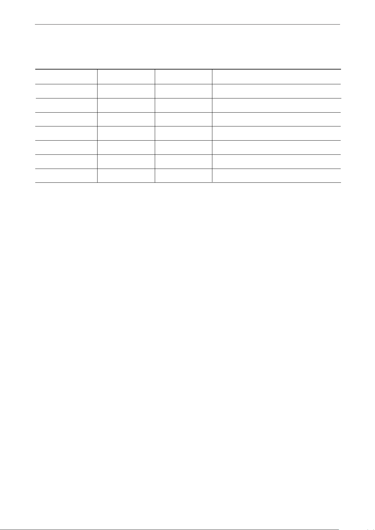
Rating Symbol Condition Value Unit
Power supply voltage V
DD
Ta = 25°C –0.3 to 7 V
Input voltage V
I
Ta = 25°C –0.3 to V
DD
+0.3 V
Output voltage V
O
Ta = 25°C –0.3 to V
DD
+0.3 V
Storage temperature range T
STG
– –55 to +150 °C
Absolute Maximum Ratings
ELECTRICAL CHARACTERISTICS
Rating Symbol Condition Value Unit
Power supply voltage V
DD
– 4.5 to 5.5 V
Clock power supply voltage V
CLK
– 2.0 to 6 V
Crystal oscillator frequency ƒ
(xt)
– 32.768 kHz
Operating temperature range T
OP
– –40 to +85 °C
Operation Range
Note: The clock power supply voltage is required to assure operation of the crystal oscillator and clock.
Rating Symbol Condition Max. Applicable pin
DC Characteristics
Typ.Min.
High input voltage (1)
Low input voltage (2)
Input leakage (1)
Input leakage (2)
High input current
Low input current
High output voltage
Low output voltage (1)
Low output voltage (2)
Leakage current
Current consumption (1)
Current consumption (2)
Input capacitance (1)
Input capacitance (2)
High input voltage (2)
V
IH1
V
IL2
I
LK1
I
LK2
I
IH
I
IL
V
OH
V
OL1
V
OL2
I
OFFLK
I
DD1
I
DD2
C
I1
C
I2
V
IH2
V
1
= V
DD
/0V
V
IH
= 0.8 V
DD
V
IL
= 0.2 V
DD
I
OH
= –400 µA
I
OL
= 2.5 mA
I
OL
= 2.5 mA
V
I
= V
DD
/0V
Oscillation at 32.768 kHz
V
DD
= 5V
CS
1
0V V
DD
= 2V
Input oscillator
Frequency 1 MHz
2.2
–
–1
–10
–100
20
2.4
–
–
–
–
–
–
–
–
–
–
–
–
–
–
–
–
–
–
–
3
5
–
–
0.2
V
DD
1
10
–20
100
–
0.4
0.4
10
30
5
–
–
–
V
µA
pF
V
µA
µA
Low input voltage (1)
V
IL1
0.8
V
DD
–
– 0.8
CS
0
, A
0
~A
3
, D
0
~ D
3
RD (E), WR (R/W),
ALE, 30-s ADJ
STOP/START
CS
1
, 68/80
CS
0
, ALE, A
0
~ A
3
,
68/80, RD (E), WR
(R/W), CS1, 30-s ADJ
D
0
~ D
3
, STOP/START
STOP/START
D
0
~ D
3
, 1Hz
INTERRUPT
PERIODIC OUT
ALARM
V
DD
Input pins other than
D
O
to D
3
D
0
to D
3
(V
DD = 5V ±10%, Ta = -40 ~ +85°C)
~
~
¡ SemiconductorMSM6542-01/02/03
74
CS
1
A
0
~ A
3
CS
0
WR
D
0
~ D
3
(Input)
V
IH2
t
C1S
t
C1H
V
IH1
V
IL1
t
RCV
t
AW
t
DH
V
IH1
V
IL1
V
IHI
= 2.2V
V
IL1
= 0.8V
5
4
1
5
V
IH2
= V
DD
V
IL2
= V
DD
V
IH2
V
IH1
V
IL1
V
IL1
V
IH1
V
IH1
V
IH1
V
IL1
t
WW
t
WA
V
IH1
V
IL1
t
DS
Rating Symbol Condition Max. Unit
–
–
–
–
–
–
–
–
(V
DD
= 5V ±10%, Ta = –40 to +85°C (in the 80 mode for the MSM6542-01/03))
80-xxx
Write mode (ALE is always at V
DD
.)
–
–
–
–
–
–
–
–
Typ.
1000
1000
20
10
120
100
10
100
Min.
t
C1S
t
C1H
t
AW
t
WA
t
WW
t
DS
t
DH
t
RCV
Switching Characteristics
CS
1
set-up time
CS
1
hold time
Address stable before WRITE
Address stabel after WRITE
WRITE pulse width
Data set-up time
Data hold time
RD/WR recovery time
ns
ns
ns
ns
ns
ns
ns
ns
–
–
–
–
–
–
–
–
¡ Semiconductor MSM6542-01/02/03
75
CS
1
A
0
~ A
3
CS
0
D
0
~ D
3
(Output)
V
IH2
t
C1S
t
C1H
V
IH1
V
IL1
t
RCV
t
DR
V
OH
V
OL
V
IH1
= 2.2V
V
IL1
= 0.8V
5
4
1
5
V
IH2
= V
DD
V
IL2
= V
DD
V
IH2
V
IH1
V
IL1
V
IL1
V
IH1
V
IH1
V
OH
V
OL
t
RA
t
RD
t
AR
"Z"
V
OH
= 2.2V
V
OL
= 0.8V
RD
Rating Symbol Condition Max. Unit
–
–
–
–
CL = 150 pF
–
–
(V
DD
= 5V ±10%, Ta = –40 to +85°C (in the 80 mode for the MSM6542-01/03))
80-xxx
Read mode (ALE is always at V
DD
.)
–
–
–
–
120
45
–
Typ.
–
–
–
–
–
–
–
Min.
1000
1000
20
20
–
10
100
t
C1S
t
C1H
t
AR
t
RA
t
RD
t
DR
t
RCV
CS
1
set-up time
CS
1
hold time
Address stable before READ
Address stable after READ
RD to data
Data hold
RD/WR recovery time
ns
ns
ns
ns
ns
ns
ns
¡ SemiconductorMSM6542-01/02/03
76
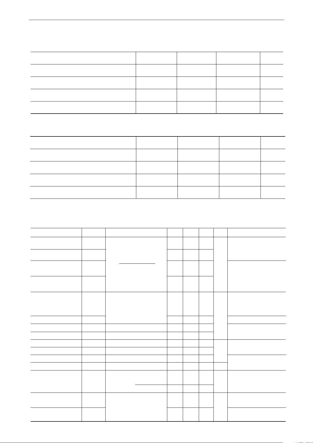
CS
1
A
0
~ A
3
CS
0
ALE
WR
D
0
~ D
3
(Input)
V
IH2
t
C1S
t
AS
t
AH
V
IH1
V
IL1
t
C1H
t
AW
t
ALW
t
WW
t
WAL
t
RCV
t
DS
t
DH
V
IH1
= 2.2V
V
IL1
= 0.8V
5
4
5
1
V
IH2
= V
DD
V
IL2
= V
DD
V
IH2
V
IH1
V
IL1
V
IH1
V
IH1
V
IL1
V
IH1
V
IL1
V
IH1
V
IL1
V
IH1
V
IH1
V
IL1
V
IH1
V
IL1
Rating Symbol Condition Max. Unit
–
–
–
–
–
–
–
–
–
–
–
(V
DD
= 5V ±10%, Ta = –40 to +85°C (in the 80 mode for the MSM6542-01/03))
80-xxx
Write mode (ALE is used.)
–
–
–
–
–
–
–
–
–
–
–
Typ.
–
–
–
–
–
–
–
–
–
–
–
Min.
1000
25
25
40
10
120
20
100
10
1000
100
t
C1S
t
AS
t
AH
t
AW
t
ALW
t
WW
t
WAL
t
DS
t
DH
t
C1H
t
RCV
CS
1
set-up time
Address set-up time
Address hold time
ALE pulse width
ALE before WRITE
WRITE pulse width
ALE after WRITE
Data set-up time
Data hold time
CS
1
hold time
RD/WR recovery time
ns
ns
ns
ns
ns
ns
ns
ns
ns
ns
ns
¡ Semiconductor MSM6542-01/02/03
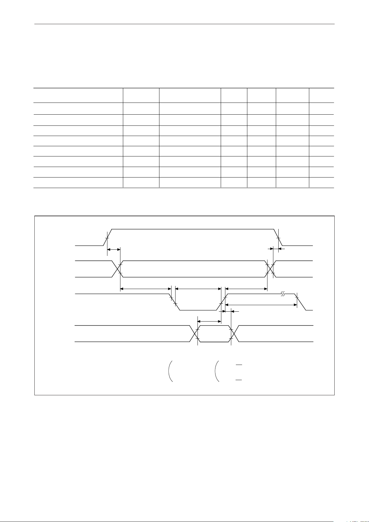
77
CS
1
A
0
~ A
3
CS
0
ALE
RD
D
0
~ D
3
(Output)
V
IH2
t
AH
t
AS
V
IH1
V
IL1
t
AW
t
RCV
t
ALR
t
RAL
t
RCV
t
RD
t
DR
V
OH
V
OL
V
IH1
= 2.2V
V
IL1
= 0.8V
5
4
5
1
t
C1S
V
IH2
= V
DD
V
IL2
= V
DD
V
OH
= 2.2V
V
OL
= 0.8V
V
IH2
V
IH1
V
IL1
t
C1H
V
IH1
V
IH1
V
IL1
V
IH1
V
IL1
V
IH1
V
IL1
V
IH1
V
IL1
"Z"
Rating Symbol Condition Max. Unit
–
–
–
–
–
–
CL = 150 pF
–
–
–
(V
DD
= 5V ±10%, Ta = –40 to +85°C (in the 80 mode for the MSM6542-01/03))
80-xxx
Read mode (ALE is used.)
–
–
–
–
–
–
120
45
–
–
Typ.
–
–
–
–
–
–
–
–
–
–
Min.
1000
25
25
40
10
20
–
10
1000
100
t
C1S
t
AS
t
AH
t
AW
t
ALR
t
RAL
t
RD
t
DR
t
C1H
t
RCV
CS
1
set-up time
Address set-up time
Address hold time
ALE pulse width
ALE before READ
ALE after READ
RD to data
Data hold
CS
1
hold time
RD/WR recovery time
ns
ns
ns
ns
ns
ns
ns
ns
ns
ns
¡ SemiconductorMSM6542-01/02/03
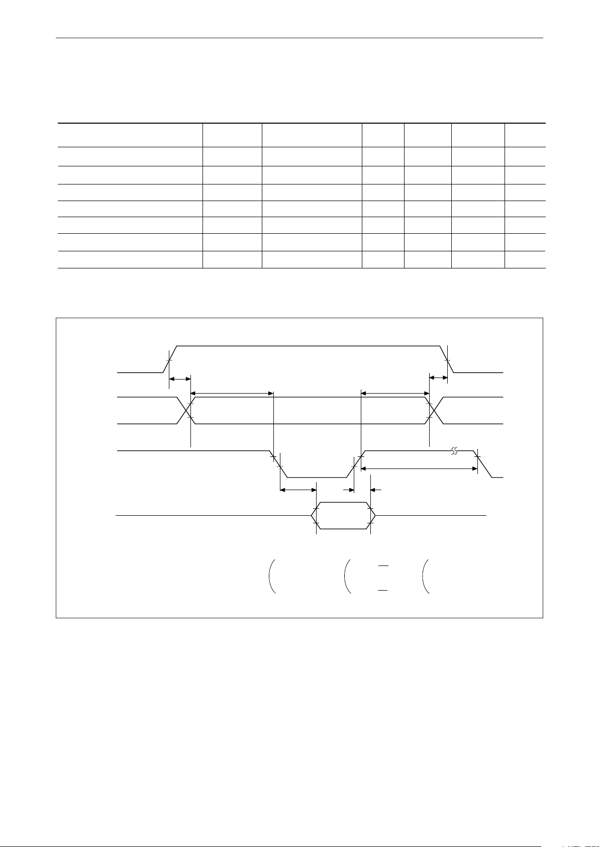
78
Rating Symbol Condition Max. Unit
–
–
–
–
–
–
–
–
CL = 150 pF
–
–
(V
DD
= 5V ±10%, Ta = 0°C to +70°C (in the 86 mode for the MSM6542-02/03))
68-xxx
–
–
–
–
–
–
–
–
120
–
–
Typ.
–
–
–
–
–
–
–
–
–
–
–
Min.
1000
100
220
20
220
500
180
20
–
10
1000
t
C1S
t
RWE
t
EHW
t
ERW
t
ELW
t
EC
t
DS
t
DHW
t
RD
t
DHR
t
C1H
CS
1
set-up time
R/W address set-up time
E 'H' pulse width
R/W address hold time
E 'L' pulse width
E cycle time
Data set-up time
WRITE data hold time
E to data
READ data hold time
CS
1
hold time
ns
ns
ns
ns
ns
ns
ns
ns
ns
ns
ns
V
IH1
= 2.2V
V
IL1
= 0.8V
WRITE mode
CS
1
R/W
CS
0
A
0
~ A
3
E
D
0
to D
3
V
IH2
t
C1S
t
C1H
V
IL1
V
IH1
t
RWE
t
EHW
t
ERW
t
ELW
t
DS
t
DHW
Input data
t
EC
READ mode
Output data
t
RD
V
OH
5
4
5
1
V
IH2
= V
DD
V
IL2
= V
DD
V
OH
= 2.2V
V
OL
= 0.8V
V
IH2
V
IL1
V
IL1
V
IH1
V
IL1
V
IL1
V
IH1
V
IH1
V
IL1
V
IL1
V
IH1
V
IL1
V
IH1
V
IL1
V
IH2
t
C1S
t
C1H
V
IH1
V
IL1
t
RWE
t
EHW
t
ERW
t
ELW
V
IH2
V
IH1
V
IH1
V
IL1
V
IH1
V
IL1
V
IH1
V
IH1
V
IL1
V
IL1
t
DHR
V
OL
V
OH
V
OL
t
EC
CS
1
R/W
CS
0
A
0
~ A
3
E
D
0
to D
3

¡ Semiconductor MSM6542-01/02/03
79
DESCRIPTION OF PINS
D
0
to D
3
(Data bus pins 0 to 3)
These input pins connected to the data bus of a microcomputer are used for the microcomputer
to read and write registers. The interface uses the positive logic. When CS
0
is low, CS
1
is high,
RD is low, and WR is high (for the 68-xxx system, CS
0
is low, CS
1
is high, R/W is high, and E is
high), these data bus pins are in the output mode. In the other cases, they are in the high
impedance status.
A
0
to A
3
(Address bus pins 0 to 3)
These input pins connected to the address bus of a microcomputer specify a register used by the
microcomputer for read or write. The address data specified by these pins is used in conjunction
with the input to the ALE pin.
ALE (Address Latch Enable)
This input pin is for address and CS
0
.
When the ALE pin is high, the address bus data and CS
0
are read into the IC. When it is low,
the address data and CS
0
read at ALE = H are retained in the IC. CS
1
functions independently
of the ALE pin.
When using an MSC-48-, MSC-51-, or 8085-based microcomputer having an ALE output pin,
connect this pin to the ALE output pin of the microcomputer. When a four-bit microcomputer
shares the four address bus pins, A
0
to A
3
, with another peripheral IC, the ALE pin on this IC
can be used to specify it.
When the microcomputer has no ALE output pin, connect the ALE input pin on this IC to the
V
DD
.
WR [R/W] (WRITE [READ/WRITE])
This input pin is connected to the WR pin for the 80-based CPU or the R/W pin for the 68-based
CPU.
RD [E] (READ [E])
This input pin is connected to the RD pin for the 80-based CPU or the E pin for the 68-based CPU.
CS
0
, CS
1
(Chip select pins 0 and 1)
These input pins enable or disable input of ALE, WR (R/W), and RD (E). When CS
0
is low and
CS
1
is high, these inputs are enabled. In the other combinations, the IC unconditionally assumes
that ALE is low and WR and RD are high (for the 68-based CPU, E is low). However, CS
0
needs
to operate in conjunction with ALE and CS
1
operates independently of ALE. Connect CS
1
to the
power supply voltage detection pin. For more information, see the descriptions in "USAGE"
and "USE OF CS
1
."
¡ SemiconductorMSM6542-01/02/03
80
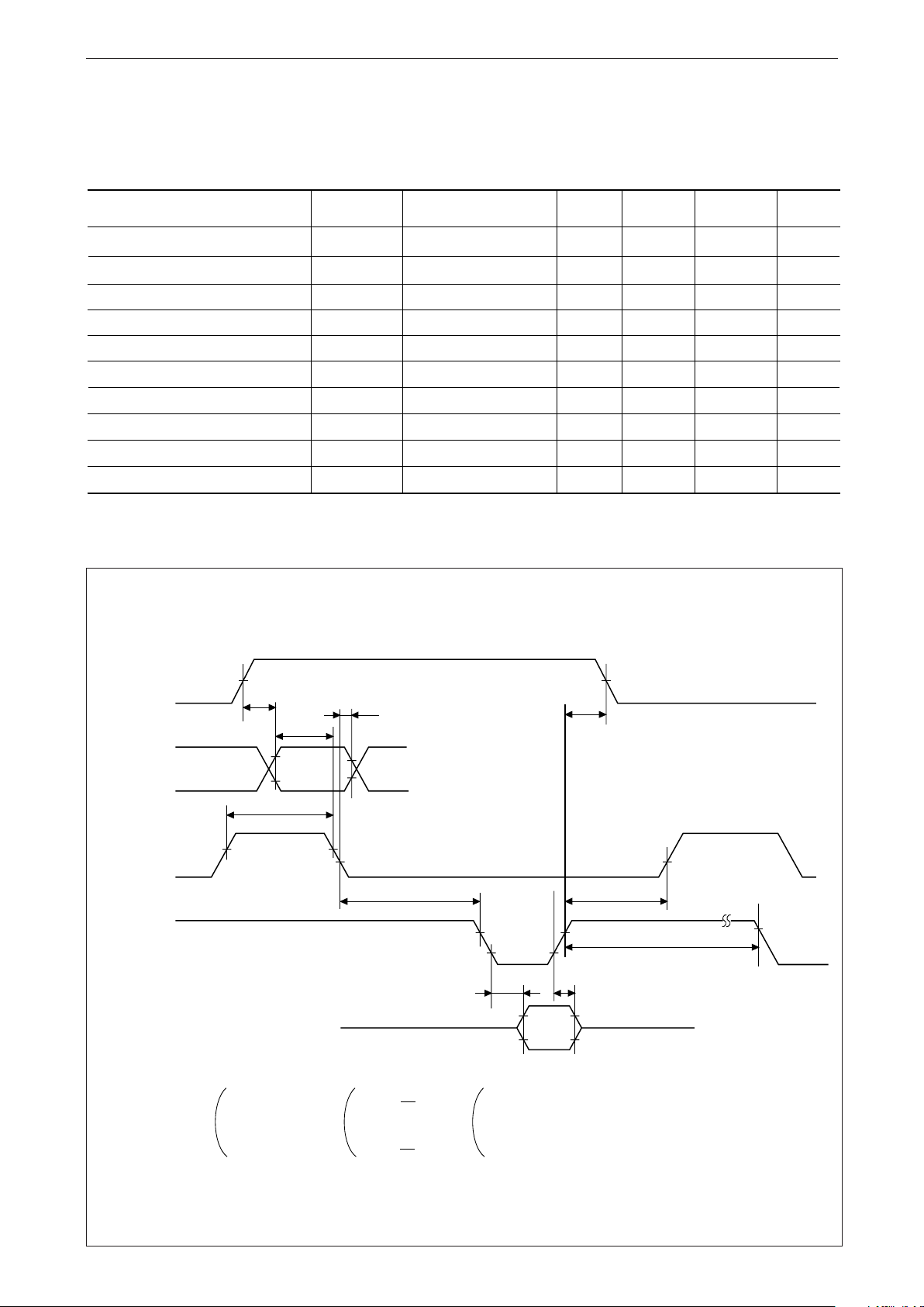
PERIODIC OUT (Only for the MSM6542-03)
This output pin is used for N-channel open drain. It outputs a single pulse or an
interrupt request as a trigger each time a carry is generated from the clock counter.
Output from this pin is not disabled by CS
0
and CS
1
.
ALARM OUT (Only for the MSM6542-03)
This output pin is used for N-channel open drain. It outputs a single pulse or an
interrupt request each time the contents of the clock counter match the date and time for
which an alarm is set. Output from this pin is not disabled by CS
0
and CS
1
.
INTERRUPT OUT (Only for the MSM6542-01/02)
This output pin is N-channel open drain. It ORs the signals from the PERIODIC OUT
and ALARM OUT pins above.
Carry trigger
PERIODIC OUT
V
DD
Date and time
matching trigger
ALARM OUT
V
DD
INTERRUPT OUT
V
DD
Carry trigger
Date and time
matching trigger
¡ Semiconductor MSM6542-01/02/03
81
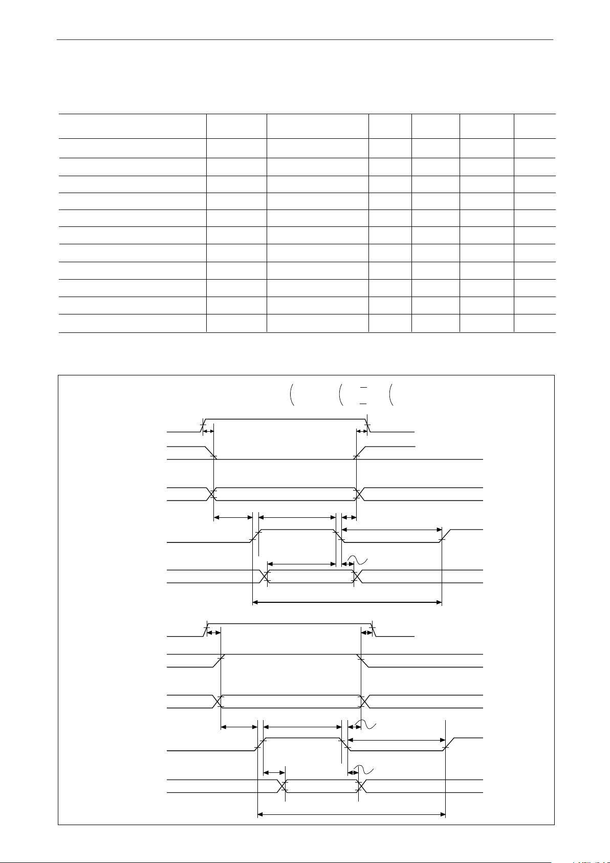
XT and XT (X'tal OSC)
These pins are the connecting terminals to connect the capacitors and crystal oscillator at
32.768kHz as shown below.
V
DD
or
GND
5M
Ω
TYP.
200KΩ
TYP.
XT
32.768
kHz
C1
C2
XT
MSM6542
Example
(Equivalent series resistance < 30 kΩ
C
1
, C
2
= 15 to 30 pF)
Note: Oscillation accuracy and allowable values of the equivalent series resistor for the
crystal oscillator depend on the value of the capacitor used for oscillation. For
selection of a crystal oscillator and the value of the capacitor needed for it,
consult the crystal oscillator manufacturer.
To supply external 32.768 kHz clocks, enter CMOS output or pulled-up TTL output to the XT
pin and leave the XT pin open.
V
DD
and V
SS
These are power supply pins. Connect the V
SS
pin to ground and supply positive power to the
V
DD
pin.
The 1 Hz, 30 sec ADJ, STOP/START, and 68/80 pins described below are used only for the
MSM6542-03.
1 Hz
This output pin is used to confirm the oscillation frequency. It outputs 1-Hz pluses at a duty
cycle of 50%.
This pin provides one-second output from the clock counter. Therefore, it is cleared to a low
when the REST bit is high or 30-second adjustment is performed. When STOP function is
performed, the output stops at whatever level the output is at that instant.
This pin provides CMOS output level, regardless of the level of the CS
1
pin. If a load is connected
to this pin during standby operation, the battery will be quickly dissipated.
=
¡ SemiconductorMSM6542-01/02/03
82
30-sec ADJ (30-seconds Adjustment)
When this input pin goes high, 30-second adjustment is performed on the rising edge. When
not used, connect to ground.
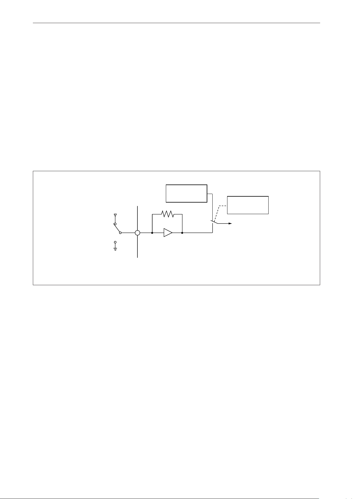
STOP/START
This input pin can be used as an integrating clock. When the pin is high, clocking at frequencies
lower than 4096 Hz stops. When the pin goes low, clocking is resumed.
The HD/SFT bit of the C
E
' register specifies whether the stop/start function is implemented by
hardware or software.
When not used, connect to ground. For more information, see the description of "C
F
register"
and "C
E
' register" in "EXPLANATION OF REGISTERS."
STOP
STOP bit of
the C
F
register
HD/SFT bit of
the C
E
' register
STOP/START
START
E
q
uivalent circuit of the STOP/START
p
in
Inside of the MSM6542
68/80
This input pin selects which CPU this IC is to be connected. To connect the IC to the 68-based
CPU, leave the pin at V
DD
. To connect the IC to the 80-based CPU, leave the pin at the ground
level.

¡ Semiconductor MSM6542-01/02/03
83
EXPLANATION OF REGISTERS
Registers R-S
1
, R-S
10
, R-MI
1
, R-MI
10
, R-H
1
, R-H
10
, R-D
1
, R-D
10
, R-MO
1
, R-MO
10
, R-Y
1
, R-Y
10
,
R-W
a) The letter R followed by a hyphen (-) in these register names indicate a realtime register. S
1
,
S
10
, MI
1
, MI
10
, H
1
, H
10
, MO
1
, MO
10
, Y
1
, Y
10
, and W are abbreviations for Second 1, Second 10,
MInute 1, MInute 10, Hour 1, Hour 10, Day 1, Day 10, MOnth 1, MOnth 10, Year 1, Year 10,
and Week. The value of each register is weighted in BCD.
b) Positive logic is used. For example, when (r-s
8
, r-s
4
, r-s
2
, r-s
1
) is (1, 0, 0, 1), it indicates 9
seconds.
c) An asterisk (*) in bank 0 in the realtime register table indicates the bit is automatically set
at 0 even though the write data is 1, when the CAL bit of the C
E
' register is high.
When the CAL bit is low, registers R-D
1
, R-D
10
, R-MO
1
, R-MO
10
, R-Y
1
, and R-Y
10
are used as
RAM areas. The bits marked * in these RAM areas can be used for write and read
operations.
For more information, see the description of "C
E
' register" in "EXPLANATION OF REG-
ISTERS."
d) Be sure not to set non-existent data in an non-RAM area, that is, realtime registers.
Otherwise, a clock error may occur.
e) r-pm/am, r-h
20
, and r-h
10
In the 12-hour clock mode, the possible hours are from 1 A.M. to 12 A.M. and from 1 P.M.
to 12 P.M. When the bit is 1, it indicates P.M. When the bit is 0, it indicates A.M. In the 24-
hour clock mode, the possible hours are from 0 o'clock to 23 o'clock.
During write operation, the r-pm/am bit is ignored in the 24-hour clock mode and the r-
h
20
bit in the 12-hour clock mode.
During read operation, the r-pm/am bit is unconditionally set at 0 in the 24-hour clock
mode and the r-h
20
bit in the 12-hour clock mode.
f) R-Y
1
and R-Y
10
The IC described in this manual operates in Gregorian years. When it operates in Japanese
calendar years (Heisei), a leap year is also automatically determined. Leap years are 1992,
1996, 2000, 2004, 2008, and so on.
¡ SemiconductorMSM6542-01/02/03
84
r-w
4
Day of the week
0
0
0
0
1
1
1
r-w
2
r-w
1
0
0
1
1
0
0
1
0
1
0
1
0
1
0
Sun
Mon
Tue
Wed
Thu
Fri
Sat
g) R-W
The R -W bits counts from 0 to 6. An example of weighting is shown in the following table.
Days are not determined from dates.
C
D
register (Control D Register)
a) MASK
1
(D
0
)
This bit controls periodic output for which a carry from the clock counter is used as a trigger.
When the bit is 0, output is provided from the INTERRUPT OUT pin for the MSM6542-01/
02 or the PERIODIC OUT pin for the MSM6542-03. When the bit 1, output is disabled.
The relationships between causes of periodic output and the status of the MASK
1
bit are
shown below. (For the MSM6542-01/02, data resulting from the ORing of periodic output
and alarm output is output to the INTERRUPT OUT pin. For convenience, however, alarm
output is ignored in the following description.)
 Loading...