


E2E0013-38-93
This version: Sep. 1998
Semiconductor MSM6404A/6404VS
¡ Semiconductor
Previous version: Mar. 1996
MSM6404A/6404VS
High speed and High performance 4-Bit Microcontroller
GENERAL DESCRIPTION
The MSM6404A microcontroller is a low-power device implemented in complementary metaloxide semiconductor technology. The MSM6404A is optimized for high-speed processing and complicated-control applications.
The MSM6404VS is a CMOS 4-bit microcontroller that employs an external EPROM using a piggy-back package in place of the program memory (ROM) internal to the MSM6404A. The MSM6404VS can be used for program development verification because the programs can be modified by programming an external EPROM 2732 equivalent or 2764A equivalent.
FEATURES
• Mask ROM (MSM6404A) |
: 4000 words ´ 8 bits |
External ROM (MSM6404VS) |
: 8196 words ´ 8 bits |
• RAM (including the stack area) |
: 256 words ´ 4 bits |
• I/O port |
: 8 ports ´ 4 bits |
Input-output port |
|
Input port |
: 1 port ´ 4 bits |
4 bits are for input ports having a latch; the other 32 bits are input/output ports that allow bit manipulation
• Three built-in counters |
: 12-bit time-base counter |
|
12-bit programmable timer |
|
8-bit high-speed programmable timer/event |
|
counter |
•Built-in 8-bit serial I/O register (with 3-bit counter)
•Five interrupts with five priority levels (4 internal, 1 external)
•32 stacks (in RAM)
•Power-down features
• Minimum instruction execution time |
: 952 ns @ 4.2 MHz clock |
|
• Instruction systems suitable for control |
|
|
• Fully static operation |
|
|
• Low power consumption |
|
|
• Single 5 V supply |
|
|
• Package options: |
|
|
MSM6404A |
|
: (Product name : MSM6404A-´´´RS) |
42-pin plastic DIP (DIP42-P-600-2.54) |
|
|
44-pin plastic QFP (QFP44-P-910-0.80-K) |
|
: (Product name : MSM6404A-´´´GS-K) |
44-pin plastic QFP (QFP44-P-910-0.80-2K) |
: (Product name : MSM6404A-´´´GS-2K) |
|
MSM6404VS
42-pin ceramic piggyback (ADIP42-C-600-2.54) : (Product name : MSM6404VS)
´´´ indicates a code number.
1/25

|
|
|
|
|
|
|
|
|
|
|
|
|
|
RAM |
|
|
|
|
|
|
|
|
|
|
|
|
|
|
|
|
|
|
|
|
|
|
|
|
|
|
|
|
|
|
|
|
|
|
|
|
|
|
|
|
|
|
|
|
|
|
|
16 ´ 16 ´ 4 bits |
|
|
|
|
|
|
|
|
|
|
|
|
|
|
|
|
|
|
|
|
|
|
|
|
|
|
|
INSTR |
|||||||||||||
|
|
|
|
|
|
|
|
|
|
|
|
|
|
|
DEC |
|
|
|
|
|
|
|
|
|
|
|
|
|
|
|
|
|
|
|
|
C |
|
|
|
|
|
ACC |
DEC |
||||||||
|
|
|
|
|
|
|
|
|
|
|
|
|
|
|
|
|
|
|
|
|
|
|
|
|
|
|
|
|
|
|
|
|
|
|
|||||||||||||||||
|
|
|
|
|
|
|
|
|
|
|
|
|
|
|
|
|
|
|
|
|
|
|
|
|
|
|
|
|
|
|
|
|
|
|
|
|
|
|
|
ALU |
|
|
|
||||||||
|
|
|
|
|
|
|
|
SP |
|
|
|
|
|
H |
|
|
|
|
|
|
L |
|
|
|
|
|
|
|
|
|
|
|
|
|
|
|
F |
||||||||||||||
|
|
|
|
|
|
|
|
|
|
|
|
|
|
|
|
|
|
|
|
|
|
|
|
|
|
|
|
|
|
|
|
|
|
|
|||||||||||||||||
|
|
|
|
|
|
|
|
|
|
|
|
|
|
|
|
|
|
|
|
|
|
|
|
|
|
|
|
|
|
|
|
|
|
|
|
|
|
|
|
|
|
||||||||||
|
|
|
|
|
|
|
|
|
|
|
|
|
|
|
|
|
|
|
|
|
|
|
|
|
|
|
|
|
|
|
|
|
|
|
|
|
|
|
|
|
|
|
|
|
|
|
|
|
|
|
|
|
|
|
|
|
|
|
|
|
|
|
|
|
|
|
|
|
|
|
|
|
|
|
|
|
|
|
|
|
|
|
|
|
|
|
|
|
|
|
|
|
|
|
|
|
|
|
|
|
|
|
|
|
|
|
|
|
|
|
|
|
|
|
|
|
|
|
|
|
|
|
|
|
|
|
|
|
|
|
|
|
|
|
|
|
|
|
|
|
|
|
|
|
|
|
|
|
|
|
|
Interrupt |
PC INTE |
||
|
|
|
|
|
|
|
|
|
|
|
|
|
|
|
12-bit Timer |
|
P9 |
8-bit T/C |
PA |
8-bit SR |
|
|
|
|
Control |
PD IRQ |
|||||||||||||||||||||||||
|
|
|
|
|
|
|
|
|
|
|
|
|
|
|
|
|
|
|
|
|
|
|
|
|
|
|
|
|
|
|
|
|
|
|
|
|
|
|
|
|
|
|
|
|
|
|
|
12-bit TBC |
|
||
|
|
|
|
|
|
|
|
|
|
|
|
|
|
|
|
|
|
|
|
|
|
|
|
|
|
|
|
|
|
|
|
|
|
|
|
|
|
|
|
|
|
|
|
|
|||||||
|
P8 |
|
P7 |
|
|
P6 |
|
P5 |
|
P4 |
|
P3 |
|
P2 |
|
|
P1 |
|
P0 |
|
|
|
|||||||||||||||||||||||||||||
|
|
|
|
|
|
|
|
|
|
|
|
|
|
||||||||||||||||||||||||||||||||||||||
|
|
|
|
|
|
|
|
|
|
|
|
|
|
|
|
|
|
|
|
|
|
|
|
|
|
|
|
|
|
|
|
|
|
|
|
|
|
|
|
|
|
|
|
|
|||||||
|
|
|
|
|
|
|
|
|
|
|
|
|
|
|
|
|
|
|
|
|
|
|
|
|
|
|
|
|
|
|
|
|
|
|
|
|
|
|
|
|
|
|
|
|
|
||||||
3 2 1 0 |
3 2 1 0 |
3 2 1 0 |
3 2 1 0 |
3 2 1 0 |
3 2 1 0 |
3 2 1 0 |
|
3 2 1 0 |
|
3 2 1 0 |
|
|
|
||||||||||||||||||||||||||||||||||||||
|
|
|
|
|
|
|
|
|
|
|
|
|
|
|
|
|
|
|
|
|
|
|
|
|
|
|
|
|
|
|
|
|
|
|
|
INT |
|
|
|
|
|
CIN |
|
|
|
|
SCK, CTO, CLK |
|
|
|
|
|
|
|
|
|
|
|
|
|
|
|
|
|
|
|
|
|
|
|
|
|
|
|
|
|
|
|
|
|
|
|
|
|
|
|
|
|
|
|
|
|
|
|
|
|
|
|
|
||||
|
|
|
|
|
|
|
|
|
|
|
|
|
|
|
|
|
|
|
|
|
|
|
|
|
|
|
|
|
|
|
|
|
|
|
|
|
|
|
|
|
|
|
|
|
|
|
SO |
|
|
|
|
|
|
|
|
|
|
|
|
|
|
|
|
|
|
|
|
|
|
|
|
|
|
|
|
|
|
|
|
|
|
|
|
|
|
|
|
|
|
|
|
|
TMO |
|
|
|
|
|
|
||||
|
|
|
|
|
|
|
|
|
|
|
|
|
|
|
|
|
|
|
|
|
|
|
|
|
|
|
|
|
|
|
|
|
|
|
|
|
|
|
|
|
|
|
|
|
|
||||||
|
|
|
|
|
|
|
|
|
|
|
|
|
|
|
|
|
|
|
|
|
|
|
|
|
|
|
|
|
|
|
|
|
|
|
|
|
|
|
TCK |
|
|
SI |
|
|
|
||||||
|
|
|
|
|
|
|
|
|
|
|
|
|
|
|
|
|
|
|
|
|
|
|
|
|
|
|
|
|
|
|
|
|
|
|
|
|
|
|
|
|
|
|
|
||||||||
2/25
ROM
4000 ´ 8 bits
DEC
11 PC 0
PB
Timing |
|
OSC0 |
||
|
||||
|
|
|
|
|
|
OSC1 |
|||
& |
|
|||
|
TEST |
|||
Control |
|
|||
|
|
|
|
|
|
RESET |
|||
|
|
|||
VDD
GND
MSM6404A |
DIAGRAM BLOCK |
Semiconductor ¡ |
MSM6404A/6404VS

|
|
|
|
|
|
|
|
|
|
|
|
|
|
RAM |
|
|
|
|
|
|
|
|
|
|
|
|
|
|
|
|
|
|
|
|
|
|
|
|
|
|
|
|
|
|
|
|
|
|
|
|
|
|
|
|
|
|
|
16 ´ 16 ´ 4 bits |
|
|
|
|
|
|
|
|
|
|
|
|
|
|
|
|
|
|
|
|
|
|
INSTR |
||||||||||||||
|
|
|
|
|
|
|
|
|
|
|
|
|
|
|
DEC |
|
|
|
|
|
|
|
|
|
|
|
|
|
|
|
|
|
|
|
|
|
C |
|
|
|
|
ACC |
DEC |
||||
|
|
|
|
|
|
|
|
|
|
|
|
|
|
|
|
|
|
|
|
|
|
|
|
|
|
|
|
|
|
|
|
|
|
|
|
|
|
|
|
||||||||
|
|
|
|
|
|
|
|
|
|
|
|
|
|
|
|
|
|
|
|
|
|
|
|
|
|
|
|
|
|
|
|
|
|
|
|
|
|
|
|
ALU |
|
|
|
||||
|
|
|
|
|
|
|
|
SP |
|
|
|
|
|
H |
|
|
|
|
|
|
|
L |
|
|
|
|
|
|
|
|
|
|
|
|
|
|
F |
||||||||||
|
|
|
|
|
|
|
|
|
|
|
|
|
|
|
|
|
|
|
|
|
|
|
|
|
|
|
|
|
|
|
|
|
|
|
|||||||||||||
|
|
|
|
|
|
|
|
|
|
|
|
|
|
|
|
|
|
|
|
|
|
|
|
|
|
|
|
|
|
|
|
|
|
|
|
|
|
||||||||||
|
|
|
|
|
|
|
|
|
|
|
|
|
|
|
|
|
|
|
|
|
|
|
|
|
|
|
|
|
|
|
|
|
|
|
|
|
|
|
|
|
|
|
|
|
|
|
|
|
|
|
|
|
|
|
|
|
|
|
|
|
|
|
|
|
|
|
|
|
|
|
|
|
|
|
|
|
|
|
|
|
|
|
|
|
|
|
|
|
|
|
|
|
|
|
|
|
|
|
|
|
|
|
|
|
|
|
|
|
|
|
|
|
|
|
|
|
|
|
|
|
|
|
|
|
|
|
|
|
|
|
|
|
|
|
|
|
|
|
|
Interrupt |
PC INTE |
||
|
|
|
|
|
|
|
|
|
|
|
|
|
|
|
|
|
|
|
|
|
|
|
|
|
|
|
|
|
|
|
|
|
|
|
|
|
|
|
|
|
|
|
|
||||
|
|
|
|
|
|
|
|
|
|
|
|
|
|
|
12-bit Timer |
|
P9 |
8-bit T/C |
PA |
8-bit SR |
|
Control |
PD IRQ |
||||||||||||||||||||||||
|
|
|
|
|
|
|
|
|
|
|
|
|
|
|
|
|
|
|
|
|
|
|
|
|
|
|
|
|
|
|
|
|
|
|
|
|
|
|
|
|
|
|
|
12-bit TBC |
|
||
|
|
|
|
|
|
|
|
|
|
|
|
|
|
|
|
|
|
|
|
|
|
|
|
|
|
|
|
|
|
|
|
|
|
|
|
|
|
|
|
|
|
|
|
|
|||
|
|
|
|
|
|
|
|
|
|
|
|
|
|
|
|
|
|
|
|
|
|
|
|
|
|
|
|
|
|
|
|
|
|
|
|
|
|
|
|
|
|
|
|
|
|||
|
|
|
|
|
|
|
|
|
|
|
|
|
|
|
|
|
|
|
|
|
|
|
|
|
|
|
|
|
|
|
|
|
|
|
|
|
|
|
|
|
|
|
|
|
|||
|
P8 |
|
P7 |
|
|
P6 |
|
P5 |
|
P4 |
|
P3 |
|
P2 |
|
|
P1 |
P0 |
|
|
|
||||||||||||||||||||||||||
|
|
|
|
|
|
|
|
|
|
|
|
|
|||||||||||||||||||||||||||||||||||
|
|
|
|
|
|
|
|
|
|
|
|
|
|
|
|
|
|
|
|
|
|
|
|
|
|
|
|
|
|
|
|
|
|
|
|
|
|
|
|
|
|
|
|
|
|
||
|
|
|
|
|
|
|
|
|
|
|
|
|
|
|
|
|
|
|
|
|
|
|
|
|
|
|
|
|
|
|
|
|
|
|
|
|
|
|
|
|
|
|
|
|
|
|
|
3 2 1 0 |
3 2 1 0 |
3 2 1 0 |
3 2 1 0 |
|
3 2 1 0 |
3 2 1 0 |
3 2 1 0 |
|
3 2 1 0 |
3 2 1 0 |
|
|
|
|
|||||||||||||||||||||||||||||||||
|
|
|
|
|
|
|
|
|
|
|
|
|
|
|
|
|
|
|
|
|
|
|
|
|
|
|
|
|
|
|
|
|
|
|
|
|
INT |
|
|
|
|
CIN |
SCK, CTO, CLK |
|
|
|
|
|
|
|
|
|
|
|
|
|
|
|
|
|
|
|
|
|
|
|
|
|
|
|
|
|
|
|
|
|
|
|
|
|
|
|
|
|
|
|
|
|
TMO |
SO |
|
|
|
||
|
|
|
|
|
|
|
|
|
|
|
|
|
|
|
|
|
|
|
|
|
|
|
|
|
|
|
|
|
|
|
|
|
|
|
|
|
|
|
|
TCK |
SI |
|
|
|
|||
3/25
|
|
|
|
|
RV |
|
I0 to I7 |
||
|
|
|
|
|
|
|
A0 to A12 |
||
|
|
|
|
|
|
|
|||
|
|
|
|
|
DV |
|
|||
12 |
|
PC |
|
|
|
|
|
|
|
|
0 |
|
|
|
|
||||
|
|
|
|
|
|
|
|
|
|
|
|
|
|
|
|
|
|
|
|
PB |
|
|
|
|
|
|
|
|
|
|
|
|
|
|
|
OSC0 |
|||
Timing |
|
|
|
||||||
|
|
|
|||||||
|
|
|
|
|
|
|
|||
|
|
|
OSC1 |
||||||
& |
|
|
|
||||||
|
|
|
TEST |
||||||
Control |
|
|
|||||||
|
|
|
|
|
|
||||
|
|
RESET |
|||||||
|
|
|
|
|
|
||||
|
|
|
|
|
|
VDD |
|||
|
|
|
|
|
|
||||
|
|
|
|
|
|
GND |
|||
|
|
|
|
|
|
||||
MSM6404VS |
(continued) DIAGRAM BLOCK |
Semiconductor ¡ |
MSM6404A/6404VS
¡ Semiconductor |
MSM6404A/6404VS |
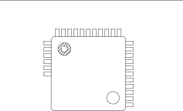
PIN CONFIGURATION (TOP VIEW)
|
|
|
|
|
|
|
|
P4.0 |
1 |
|
42 |
VDD |
|
|
P4.1 |
|
|
|
P5.3 |
|
2 |
41 |
|||||
|
P4.2 |
|
|
|
P5.2 |
|
3 |
40 |
|||||
|
P4.3 |
|
|
|
P5.1 |
|
4 |
39 |
|||||
|
P3.0 |
|
|
|
P5.0 |
|
5 |
38 |
|||||
|
|
|
|
|
|
|
|
P3.1 |
6 |
|
37 |
P6.3 |
|
|
|
|
|
|
|
|
|
P3.2 |
7 |
|
36 |
P6.2 |
|
|
|
|
|
|
|
|
|
P3.3 |
8 |
|
35 |
P6.1 |
|
|
|
|
|
|
|
|
|
OSC0 |
9 |
|
34 |
P6.0 |
|
|
|
|
|
|
|
|
|
OSC1 |
|
10 |
|
33 |
P7.3 |
|
|
|||||
RESET |
11 |
|
32 |
P7.2 |
||
|
|
|
|
|
|
|
|
TEST |
12 |
|
31 |
P7.1 |
|
|
|
|
|
|
|
|
|
P2.0 |
13 |
|
30 |
P7.0 |
|
|
|
|
|
|
|
|
|
P2.1 |
14 |
|
29 |
P8.3 |
|
|
|
|
|
|
|
|
|
P2.2 |
15 |
|
28 |
P8.2 |
|
|
|
|
|
|
|
|
|
P2.3 |
16 |
|
27 |
P8.1 |
|
|
|
|
|
|
|
|
|
P0.0 |
17 |
|
26 |
P8.0 |
|
|
P0.1 |
|
|
|
P1.3 |
|
|
18 |
|
25 |
|||
|
|
|
|
|
|
|
|
P0.2 |
19 |
|
24 |
P1.2 |
|
|
|
|
|
|
|
|
|
P0.3 |
20 |
|
23 |
P1.1 |
|
|
GND |
21 |
|
22 |
P1.0 |
|
|
|
|
|
|
|
|
42-Pin Plastic DIP
4/25
¡ Semiconductor MSM6404A/6404VS
PIN CONFIGURATION (TOP VIEW) (continued)
|
|
|
|
|
P3.0 |
|
P4.3 |
|
P4.2 |
|
P4.1 |
|
P4.0 |
|
V |
|
P5.3 |
|
P5.2 |
|
P5.1 |
|
P5.0 |
|
P6.3 |
|
|
|
|
|
|
|
|
|
|
|
|
|
|
|
|
|
DD |
|
|
|
|
|
|
|
|
|
|
|
|
|
|
|
44 |
43 |
42 |
41 |
40 |
39 |
38 |
37 |
36 |
35 |
34 |
|
|
||||||||||||
|
P3.1 |
1 |
|
|
|
|
|
|
|
|
|
|
|
|
|
|
|
|
|
|
|
|
33 |
P6.2 |
|||
|
P3.2 |
2 |
|
|
|
|
|
|
|
|
|
|
|
|
|
|
|
|
|
|
|
|
32 |
P6.1 |
|||
|
P3.3 |
3 |
|
|
|
|
|
|
|
|
|
|
|
|
|
|
|
|
|
|
|
|
31 |
P6.0 |
|||
|
OSC0 |
4 |
|
|
|
|
|
|
|
|
|
|
|
|
|
|
|
|
|
|
|
|
30 |
NC |
|||
|
|
|
5 |
|
|
|
|
|
|
|
|
|
|
|
|
|
|
|
|
|
|
|
|
29 |
P7.3 |
||
|
OSC1 |
|
|
|
|
|
|
|
|
|
|
|
|
|
|
|
|
|
|
|
|
||||||
RESET |
6 |
|
|
|
|
|
|
|
|
|
|
|
|
|
|
|
|
|
|
|
|
28 |
P7.2 |
||||
|
TEST |
|
|
|
|
|
|
|
|
|
|
|
|
|
|
|
|
|
|
|
|
|
27 |
P7.1 |
|||
7 |
|
|
|
|
|
|
|
|
|
|
|
|
|
|
|
|
|
|
|
|
|||||||
|
P2.0 |
|
|
|
|
|
|
|
|
|
|
|
|
|
|
|
|
|
|
|
|
|
26 |
P7.0 |
|||
8 |
|
|
|
|
|
|
|
|
|
|
|
|
|
|
|
|
|
|
|
|
|||||||
|
P2.1 |
|
|
|
|
|
|
|
|
|
|
|
|
|
|
|
|
|
|
|
|
|
25 |
P8.3 |
|||
9 |
|
|
|
|
|
|
|
|
|
|
|
|
|
|
|
|
|
|
|
|
|||||||
|
P2.2 |
|
|
|
|
|
|
|
|
|
|
|
|
|
|
|
|
|
|
|
|
|
24 |
P8.2 |
|||
10 |
|
|
|
|
|
|
|
|
|
|
|
|
|
|
|
|
|
|
|
|
|||||||
|
P2.3 |
|
|
|
|
|
|
|
|
|
|
|
|
|
|
|
|
|
|
|
|
|
23 |
P8.1 |
|||
11 |
|
|
|
|
|
|
|
|
|
|
|
|
|
|
|
|
|
|
|
|
|||||||
|
|
|
|
|
|
|
|
|
|
|
|
|
|
|
|
|
|
|
|
|
|
|
|
|
|
|
|
|
|
|
|
12 |
|
13 |
|
14 |
|
15 |
|
16 |
|
17 |
|
18 |
|
19 |
|
20 |
|
21 |
|
22 |
|
|
|
|
|
|
|
|
|
|
|
|
|
|
|
|
|
|
|
|
|
|
|
|
|
|
|
|
|
|
|
|
|
|
|
|
P0.0 |
|
P0.1 |
|
P0.2 |
|
P0.3 |
|
GND |
|
NC |
|
P1.0 |
|
P1.1 |
|
P1.2 |
|
P1.3 |
|
P8.0 |
|
|
NC: No-connection pin
44-Pin Plastic QFP
5/25
¡ Semiconductor |
MSM6404A/6404VS |
PIN CONFIGURATION (TOP VIEW) (continued)
|
|
|
|
|
|
|
|
|
|
|
P4.0 |
1 |
|
|
|
42 |
|
VDD |
|
|
|
|
|
qVPP/VDD |
VDD@8 |
|
|
||
|
P4.1 |
2 |
|
41 |
|
P5.3 |
|||
|
|
|
|
wA12 |
PGM/VDD@7 |
|
|
||
|
|
|
|
|
|
||||
|
P4.2 |
3 |
|
40 |
|
P5.2 |
|||
|
|
|
|
eA7 |
VDD@6 |
|
|
||
|
|
|
|
|
|
||||
|
P4.3 |
4 |
|
39 |
|
P5.1 |
|||
|
|
|
|
rA6 |
A8@5 |
|
|
||
|
|
|
|
|
|
||||
|
P3.0 |
5 |
38 |
|
P5.0 |
||||
|
|
|
|||||||
|
|
|
|
tA5 |
A9@4 |
|
|
||
|
|
|
|
|
|
||||
|
P3.1 |
6 |
37 |
|
P6.3 |
||||
|
|
|
|||||||
|
|
|
|
yA4 |
A11@3 |
|
|
||
|
|
|
|
|
|
||||
|
P3.2 |
7 |
36 |
|
P6.2 |
||||
|
|
|
|||||||
|
|
|
|
uA3 |
OE/GND@2 |
|
|
||
|
|
|
|
|
|
||||
|
P3.3 |
8 |
35 |
|
P6.1 |
||||
|
|
|
|||||||
|
|
|
|
iA2 |
A10@1 |
|
|
||
|
|
|
|
|
|
||||
|
OSC0 |
9 |
34 |
|
P6.0 |
||||
|
|
|
|||||||
|
|
|
|
oA1 |
CE/GND@0 |
|
|
||
|
|
|
|
|
|
||||
|
OSC1 |
|
10 |
|
33 |
|
P7.3 |
||
|
|
|
|
!A0 |
I7!9 |
|
|
||
|
|
|
|
|
|
||||
RESET |
11 |
32 |
|
P7.2 |
|||||
|
|
||||||||
|
|
|
|
!1I0 |
I6!8 |
|
|
||
|
|
|
|
|
|
||||
|
TEST |
12 |
31 |
|
P7.1 |
||||
|
|
|
|||||||
|
|
|
|
!2I1 |
I5!7 |
|
|
||
|
|
|
|
|
|
||||
P2.0/INT |
13 |
30 |
|
P7.0 |
|||||
|
|
||||||||
|
|
|
|
!I23 |
I4!6 |
|
|
||
|
|
|
|
|
|
||||
|
P2.1 |
14 |
29 |
|
P8.3 |
||||
|
|
|
|||||||
|
|
|
|
!GND4 |
I3!5 |
|
|
||
|
|
|
|
|
|
||||
|
P2.2 |
15 |
|
28 |
|
P8.2 |
|||
|
|
|
|||||||
|
|
|
|
|
|
|
|
||
|
P2.3 |
16 |
|
|
27 |
|
P8.1 |
||
|
|
|
|
|
|
|
|
||
|
P0.0 |
17 |
|
|
26 |
|
P8.0 |
||
P0.1/SCK |
|
|
|
|
|
||||
18 |
|
|
25 |
|
P1.3 |
||||
|
|
|
|
|
|
|
P1.2/TCK |
||
P0.2/SO |
19 |
|
|
24 |
|
||||
|
|
|
|
|
|
|
P1.1/TMO |
||
P0.3/SI |
20 |
|
|
23 |
|
||||
|
|
|
|
|
|
|
P1.0/CIN |
||
|
GND |
21 |
|
|
22 |
|
|||
|
|
|
|
|
|
|
|
|
|
42-Pin Ceramic Piggyback
6/25

¡ Semiconductor MSM6404A/6404VS
PIN DESCRIPTIONS
Symbol |
Type |
Description |
During reset |
|
|
|
|
|
|
P0.0 |
|
|
|
|
P0.1/SCK |
I/O |
P0.1 is shared with serial clock (SCK) input/output. |
"1" |
|
P0.2/SO |
P0.2 is shared with serial data (SO) output. |
|||
|
|
|||
P0.3/SI |
|
P0.3 is shared with serial data (SI) input. |
|
|
|
|
|
|
|
P1.0/CIN |
|
P1.0 is shared with counter input (CIN). |
|
|
P1.1/TMO |
I/O |
P1.1 is shared with timer output (TMO). |
"1" |
|
P1.2/TCK |
P1.2 is shared with timer clock input (TCK). |
|||
|
|
|||
P1.3 |
|
|
|
|
|
|
|
|
|
P2.0/INT |
|
P2.0 is shared with external interrupt input (INT). |
|
|
P2.1 |
I |
|
The latch is |
|
P2.2 |
Input port with a latch, built-in pull-up resistor |
reset. |
||
|
||||
P2.3 |
|
|
|
|
|
|
|
|
|
P3.0 to 3.3 |
I/O |
— |
"1" |
|
|
|
|
|
|
P4.0 to 4.3 |
I/O |
8-bit output ports (at OPT instruction execution) |
"0" |
|
|
|
|||
P5.0 to 5.3 |
I/O |
|||
|
|
|||
|
|
|
|
|
P6.0 to 6.3 |
I/O |
— |
"0" |
|
|
|
|
|
|
P7.0 to 7.3 |
I/O |
— |
"0" |
|
|
|
|
|
|
P8.0 to 8.3 |
I/O |
— |
"0" |
|
|
|
|
|
|
OSC0 |
I |
Crystal connection pins for clock oscillation |
Oscillation |
|
OSC1 |
O |
waveform |
||
|
||||
TEST |
O |
(Test pin for manufacturer) |
Pulse output |
|
|
|
|
|
|
RESET |
I |
Input pin for system reset |
— |
|
|
|
|
|
|
VDD |
— |
Power supply voltage pins |
— |
|
GND |
||||
|
|
|
||
|
|
|
|
Note: 1. The ports except for pins P2.0 to P2.3 are pseudo bidirectional ports.
2.When each port is used for output, the MSM6404A can drive one TTL (one input) and the MSM6404VS can drive one LS TTL (one input).
Upper Pins for MSM6404VS
Symbol |
Type |
Description |
|
|
|
|
|
A0 to A12 |
O |
Address output |
|
|
|
|
|
I0 to I7 |
I |
Data input |
|
|
|
|
|
CE/GND |
I |
Chip enable input |
|
|
|
|
|
OE/GND |
I |
Output enable input |
|
|
|
|
|
PGM/VDD |
I |
Program input |
|
VDD |
— |
Power supply voltage pins |
|
GND |
|||
|
|
||
|
|
|
|
VPP/VDD |
— |
Programed power supply voltage pin |
7/25

¡ Semiconductor MSM6404A/6404VS
ABSOLUTE MAXIMUM RATINGS (MSM6404A)
Parameter |
Symbol |
Condition |
Rating |
Unit |
|
|
|
|
|
|
|
Power Supply Voltage |
VDD |
|
–0.3 to +7 |
V |
|
Input Voltage |
VI |
Ta = 25°C |
–0.3 to VDD |
V |
|
Output Voltage |
VO |
|
–0.3 to VDD |
V |
|
Power Dissipation |
PD |
Ta = 25°C per package |
200 max. |
mW |
|
|
|
|
|||
Ta = 25°C per output |
50 max. |
mW |
|||
|
|
||||
|
|
|
|
|
|
Storage Temperature |
TSTG |
— |
–55 to +150 |
°C |
RECOMMENDED OPERATING CONDITIONS (MSM6404A)
Parameter |
Symbol |
Condition |
Range |
Unit |
|||
|
|
|
|
|
|
||
Power Supply Voltage |
VDD |
fOSC £ 1 MHz |
3 to |
6 |
V |
||
fOSC £ 4.2 |
MHz |
4.5 to |
5.5 |
V |
|||
|
|
||||||
Data-Hold Voltage |
VDDH |
fOSC = 0 |
Hz |
2 to |
6 |
V |
|
Operating Temperature |
Top |
— |
|
–40 to |
+85 |
°C |
|
Fan Out |
N |
MOS load |
15 |
|
— |
||
|
|
|
|
||||
TTL load |
1 |
|
|||||
|
|
|
|
||||
|
|
|
|
|
|
|
|
Note: Refer to the fOSC-VDD characteristic in OPERATING CHARACTERISTICS for the relation-ship between power supply voltage and operating frequency.
8/25
 Loading...