


E2E0031-38-95
This version: Sep. 1998
Semiconductor MSM64158A/64158AL
¡ Semiconductor
Previous version: Mar. 1996
MSM64158A/64158AL
4-Bit Microcontroller with Built-in LCD Driver and Melody Circuit
GENERAL DESCRIPTION
The MSM64158A (1.5 V)/64158AL (3.0 V) is a high-performance 4-bit microcontroller that incroporates Oki-original CPU core nX-4/20.
The MSM64158A/64158AL has an LCD driver for up to 144 segments, an event counter, and a melody circuit. It is best suited for applications such as clocks and LCD games.
FEATURES
• Operating range |
|
|
Operating voltage |
: |
1.5 V/3.0 V |
Operating temperature |
: –40 to +70°C |
|
Operating frequency |
: 32.768 kHz crystal oscillation |
|
|
|
Approx. 32 kHz RC oscillation |
Supply current (Typ.) |
: 0.9 A (3.0 V at HALT mode) |
|
• Minimum instruction execution time |
: |
91 s |
• General memory space |
: |
2528 bytes |
• Local memory space |
: |
128 nibbles |
• LCD drivers |
: |
40 |
|
|
Common driver ´ 4 |
|
|
Segment driver ´ 36 |
|
|
1/4 duty, 1/3 bias; 144 segments (36 ´ 4) |
|
|
1/3 duty, 1/3 bias; 108 segments (36 ´ 3) |
• I/O port |
|
1 port ´ 4 bits (open drain output/CMOS output |
Input-output port |
: |
|
|
|
selectable; pull-down resistor input/high- |
|
|
impedance input selectable) |
Input port |
: |
1 port ´ 2 bits (pull-down resistor input /high- |
|
|
impedance input selectable) |
|
|
1 port ´ 4 bits (pull-down resistor input/high- |
|
|
impedance input selectable) |
• Event counter |
: |
1 |
• Melody output |
: |
1 |
• Interrupts |
: 7 sources (external 3, time base 3, melody 1) |
|
• Package: |
|
|
64-pin plastic QFP (QFP64-P-1414-0.80-BK): (Product name : MSM64158A-´´´GS-BK,
|
MSM64158AL-´´´GS-BK) |
Chip |
: MSM64158A-´´´, MSM64158AL-´´´ |
´´´indicates a code number.
•OTP version (for program evaluation) : MSM64P155/64P155L
(The packages, power polarity, and operating voltage of the MSM64P155/64P155L are different from the MSM64158A/64158AL. For details, refer to the "MSM64P155 User's Manual".)
1/25

¡ Semiconductor |
MSM64158A/64158AL |
BLOCK DIAGRAM
MIEF HALT BSR

TR2 |
TR0 |
|
|
TR1 |
|
|
|
(4) |
|
|
|
ROM |
|
|
PCM |
PCL |
PCH |
2528B |
||
|
|
|
||||
C |
ALU |
|
|
|
A8 to A11 |
|
|
|
|
|
|
||
|
|
|
|
A7 to A0 |
|
|
|
(4) |
(4) |
|
|
RAM |
|
B A |
L |
X Y |
128N |
|||
|
H |
VVV C2C1SS3SS2SS1
BIAS
ADDRESSPORT
 COM1
COM1
 COM2
COM2
 COM3
COM3
 COM4
COM4
LCD  SEG0
SEG0
 SEG35
SEG35
OSC0 |
OSC |
TIMING |
SP |
||
OSC1 |
CONTROLLER |
|
|||
|
|
|
IR DECODER |
||
RESET |
RST |
TBC |
3 |
||
|
|||||
|
|
||||
|
|
|
|||
|
|
|
INT |
|
|
TST1 |
TST |
|
|
|
|
TST2 |
|
|
|
||
|
|
|
|
||
VSSL |
VR |
|
|
|
|
VDD |
|
BUP |
|
CAPR |
|
is the CPU core (nX-4/20).
DB7 to DB0 |
(8) |
|
|
|
|
|
|
|||
|
|
|
ROMR |
|
INTC |
|
|
|
MD0 |
|
|
|
|
|
|
|
|
|
|
||
|
|
|
|
|
|
|
|
|
|
|
|
|
|
|
|
|
|
|
|
|
MD0 |
|
|
|
|
|
|
|
|
|
|
MD0 |
|
|
|
IR |
(8) |
|
|
|
|
|
INT |
|
|
|
|
|
|
|
|
|
|
|
|
PORT ADDRESS |
|
|
|
|
|
|
|||
|
|
DB7 to DB0 |
|
|
|
|
|
|
|
|
|
|
|
INT |
|
|
INT |
|
|
|
INT |
PORT2 |
EVENT |
PORT3 |
PORT6 |
|||||||
P2.0 |
P2.1 |
P2.2 |
P2.3 |
|
P3.0 |
P3.1 |
P6.0 |
P6.1 |
P6.2 |
P6.3 |
2/25
¡ Semiconductor |
MSM64158A/64158AL |
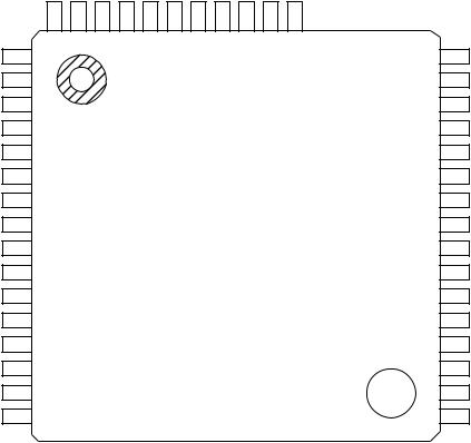
PIN CONFIGURATION (TOP VIEW)
SEG23 1 SEG22 2 SEG21 3 SEG20 4 SEG19 5 SEG18 6
SEG17 7
SEG16 8
SEG15 9
SEG14 10
SEG13 11 SEG12 12 SEG11 13 SEG10 14 SEG9 15 SEG8 16
SEG24 |
SEG25 |
SEG26 |
SEG27 |
SEG28 |
SEG29 |
SEG30 |
SEG31 |
SEG32 |
SEG33 |
SEG34 |
SEG35 |
MD0 |
|
MD0 |
|
TST1 |
|
TST2 |
|
|
|
|
|
|
|
|
|
|
|
|
|
|
|
|
|
|
|
|
|
64 |
63 |
62 |
61 |
60 |
59 |
58 |
57 |
56 |
55 |
54 |
53 |
|
52 |
|
51 |
|
50 |
|
49 |
|
|
|
|
|
|
|
|
|
|
|
|
|
|
|
|
|
|
|
|
17 |
|
18 |
|
19 |
|
20 |
|
21 |
|
22 |
|
23 |
|
24 |
|
25 |
|
26 |
|
27 |
|
28 |
|
29 |
|
30 |
|
31 |
|
32 |
|
|
|
|
|
|
|
|
|
|
|
|
|
|
|
|
|
|
|
|
|
|
|
|
|
|
|
|
|
|
|
SEG7 |
|
SEG6 |
|
SEG5 |
|
SEG4 |
|
SEG3 |
|
SEG2 |
|
SEG1 |
|
SEG0 |
|
COM4 |
|
COM3 |
|
COM2 |
|
COM1 |
|
C2 |
|
C1 |
|
V |
|
V |
|
|
|
|
|
|
|
|
|
|
|
|
|
|
|
|
|
|
|
|
|
|
|
|
|
|
|
|
SS3 |
|
SS2 |
64-Pin Plastic QFP
48 P6.0
47 P6.1
46 P6.2
45 P6.3
44 VDD
43 P2.0
42 P2.1
41 P2.2
40 P2.3
39 P3.0
38 P3.1
37 RESET
36 VSSL
35 OSC1
34 OSC0
33 VSS1
3/25
¡ Semiconductor |
MSM64158A/64158AL |
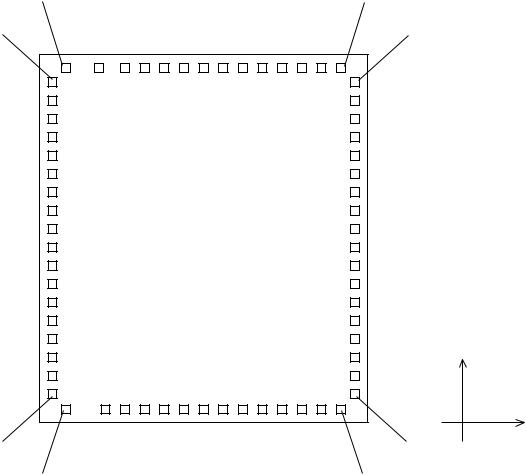
PAD CONFIGURATION
Pad Layout
46 |
33 |
47 |
32 |
Y
X
64 |
15 |
1 |
14 |
Chip Size |
: 3.63 mm ´ 3.99 mm |
Chip Thickness |
: 350 mm (typ.) |
Coordinate Origin |
: Chip center |
Pad Hole Size |
: 110 mm ´ 110 mm |
Pad Size |
: 120 mm ´ 120 mm |
Minimum Pad Pitch |
: 180 mm |
Note: The chip substrate voltage is VDD.
4/25
¡ Semiconductor |
|
|
|
|
MSM64158A/64158AL |
|||
Pad Coordinates |
|
|
|
|
|
|
|
|
|
|
|
|
|
|
|
|
|
Pad No. |
Pad Name |
X (µm) |
Y (µm) |
|
Pad No. |
Pad Name |
X (µm) |
Y (µm) |
|
|
|
|
|
|
|
|
|
1 |
MD0 |
–1344 |
–1794 |
|
41 |
COM2 |
–88 |
1794 |
|
|
|
|
|
|
|
|
|
2 |
MD0 |
–1008 |
–1794 |
|
42 |
COM1 |
–274 |
1794 |
|
|
|
|
|
|
|
|
|
3 |
SEG35 |
–824 |
–1794 |
|
43 |
C2 |
–461 |
1794 |
|
|
|
|
|
|
|
|
|
4 |
SEG34 |
–639 |
–1794 |
|
44 |
C1 |
–647 |
1794 |
|
|
|
|
|
|
|
|
|
5 |
SEG33 |
–453 |
–1794 |
|
45 |
VSS3 |
–1019 |
1794 |
6 |
SEG32 |
–267 |
–1794 |
|
46 |
VSS2 |
–1496 |
1794 |
7 |
SEG31 |
–82 |
–1794 |
|
47 |
VSS1 |
–1664 |
1671 |
8 |
SEG30 |
104 |
–1794 |
|
48 |
OSC0 |
–1664 |
1473 |
|
|
|
|
|
|
|
|
|
9 |
SEG29 |
289 |
–1794 |
|
49 |
OSC1 |
–1664 |
1275 |
|
|
|
|
|
|
|
|
|
10 |
SEG28 |
475 |
–1794 |
|
50 |
VSSL |
–1664 |
1077 |
11 |
SEG27 |
660 |
–1794 |
|
51 |
RESET |
–1664 |
879 |
|
|
|
|
|
|
|
|
|
12 |
SEG26 |
846 |
–1794 |
|
52 |
P3.1 |
–1664 |
681 |
|
|
|
|
|
|
|
|
|
13 |
SEG25 |
1031 |
–1794 |
|
53 |
P3.0 |
–1664 |
475 |
|
|
|
|
|
|
|
|
|
14 |
SEG24 |
1216 |
–1794 |
|
54 |
P2.3 |
–1664 |
285 |
|
|
|
|
|
|
|
|
|
15 |
SEG23 |
1664 |
–1689 |
|
55 |
P2.2 |
–1664 |
87 |
|
|
|
|
|
|
|
|
|
16 |
SEG22 |
1664 |
–1491 |
|
56 |
P2.1 |
–1664 |
–111 |
|
|
|
|
|
|
|
|
|
17 |
SEG21 |
1664 |
–1293 |
|
57 |
P2.0 |
–1664 |
–309 |
|
|
|
|
|
|
|
|
|
18 |
SEG20 |
1664 |
–1095 |
|
58 |
VDD |
–1664 |
–507 |
19 |
SEG19 |
1664 |
–891 |
|
59 |
P6.3 |
–1664 |
–705 |
|
|
|
|
|
|
|
|
|
20 |
SEG18 |
1664 |
–699 |
|
60 |
P6.2 |
–1664 |
–903 |
|
|
|
|
|
|
|
|
|
21 |
SEG17 |
1664 |
–501 |
|
61 |
P6.1 |
–1664 |
–1101 |
|
|
|
|
|
|
|
|
|
22 |
SEG16 |
1664 |
–303 |
|
62 |
P6.0 |
–1664 |
–1299 |
|
|
|
|
|
|
|
|
|
23 |
SEG15 |
1664 |
–105 |
|
63 |
TST2 |
–1664 |
–1497 |
|
|
|
|
|
|
|
|
|
24 |
SEG14 |
1664 |
93 |
|
64 |
TST1 |
–1664 |
–1703 |
|
|
|
|
|
|
|
|
|
25 |
SEG13 |
1664 |
291 |
|
|
|
|
|
|
|
|
|
|
|
|
|
|
26 |
SEG12 |
1664 |
489 |
|
|
|
|
|
|
|
|
|
|
|
|
|
|
27 |
SEG11 |
1664 |
687 |
|
|
|
|
|
|
|
|
|
|
|
|
|
|
28 |
SEG10 |
1664 |
885 |
|
|
|
|
|
|
|
|
|
|
|
|
|
|
29 |
SEG9 |
1664 |
1083 |
|
|
|
|
|
|
|
|
|
|
|
|
|
|
30 |
SEG8 |
1664 |
1281 |
|
|
|
|
|
|
|
|
|
|
|
|
|
|
31 |
SEG7 |
1664 |
1479 |
|
|
|
|
|
|
|
|
|
|
|
|
|
|
32 |
SEG6 |
1664 |
1677 |
|
|
|
|
|
|
|
|
|
|
|
|
|
|
33 |
SEG5 |
1395 |
1794 |
|
|
|
|
|
|
|
|
|
|
|
|
|
|
34 |
SEG4 |
1216 |
1794 |
|
|
|
|
|
|
|
|
|
|
|
|
|
|
35 |
SEG3 |
1030 |
1794 |
|
|
|
|
|
|
|
|
|
|
|
|
|
|
36 |
SEG2 |
844 |
1794 |
|
|
|
|
|
|
|
|
|
|
|
|
|
|
37 |
SEG1 |
657 |
1794 |
|
|
|
|
|
|
|
|
|
|
|
|
|
|
38 |
SEG0 |
471 |
1794 |
|
|
|
|
|
|
|
|
|
|
|
|
|
|
39 |
COM4 |
285 |
1794 |
|
|
|
|
|
|
|
|
|
|
|
|
|
|
40 |
COM3 |
98 |
1794 |
|
|
|
|
|
|
|
|
|
|
|
|
|
|
5/25

¡ Semiconductor MSM64158A/64158AL
PIN DESCRIPTIONS
Basic Functions
Function |
Pin |
Pad |
Symbol |
Type |
Description |
|
|
|
|
|
|
|
|
|
44 |
58 |
VDD |
— |
Digital power supply (0 V) |
|
|
33 |
47 |
VSS1 |
— |
Digital negative power supply (for 1.5 V spec.) |
|
|
|
|
|
|
Bias output for LCD drive (for 3.0 V spec.) |
|
|
32 |
46 |
VSS2 |
— |
Digital negative power supply (for 3.0 V spec.) |
|
Power |
|
|
|
|
Bias output for LCD drive (for 1.5 V spec.) |
|
|
|
|
|
|
|
|
Supply |
31 |
45 |
VSS3 |
— |
Bias output for LCD drive (–4.5 V) |
|
|
||||||
|
30 |
44 |
C1 |
— |
Capacitor connection pins for LCD drive bias generation. |
|
|
|
|
|
|
|
|
|
29 |
43 |
C2 |
— |
|
|
|
|
|
|
|
|
|
|
36 |
50 |
VSSL |
— |
Negative power supply pin for internal logic |
|
|
|
|
|
|
(An internally generated constant voltage is present at this pin.) |
|
|
34 |
48 |
OSC0 |
I |
Clock oscillation input and output pins: |
|
Oscillation |
|
|
|
|
Either a crystal (32.768 kHz) and a capacitor (10 to 30 pF) |
|
|
|
OSC1 |
|
|||
|
35 |
49 |
O |
are connected to these pins or a resistor (1 MW) is. |
|
|
Test |
50 |
64 |
TST1 |
I |
Input pins for test. |
|
|
|
|
|
|
|
|
49 |
63 |
TST2 |
I |
|
|
|
|
|
|
||||
|
|
|
|
|
|
|
|
37 |
51 |
RESET |
I |
System reset input pin: |
|
|
|
|
|
|
Setting this pin to "H" level puts this device into a reset state. |
|
Reset |
|
|
|
|
Then, setting this pin to "L" level starts executing an instruction |
|
|
|
|
|
from address 000H. |
||
|
|
|
|
|
||
|
|
|
|
|
This pin is internally connected to VSS1 or VSS2 through a pull- |
|
|
|
|
|
|
down resistor. |
|
|
|
|
|
|
|
|
6/25
¡ Semiconductor |
|
|
MSM64158A/64158AL |
|||||
Basic Functions (continued) |
|
|
|
|
|
|||
|
|
|
|
|
|
|
|
|
Function |
Pin |
Pad |
Symbol |
Type |
Description |
|||
|
|
|
|
|
|
|
|
|
|
43 |
57 |
P2.0 |
I |
4-bit input port (port 2): Select between pull-down resistor |
|||
|
|
|
|
|
input and high impedance input for each bit with the port 2 control |
|||
|
42 |
56 |
P2.1 |
|
||||
|
|
register (P2CON). When configured for secondary function, |
||||||
|
|
|
|
|
||||
|
41 |
55 |
P2.2 |
|
an external interrupt and capture circuit trigger input are allocated. |
|||
|
|
If P2.0 to P2.3 are all set to a "H" level, the device enters system |
||||||
|
|
|
|
|
||||
|
40 |
54 |
P2.3 |
|
||||
|
|
reset mode. |
||||||
|
|
|
|
|
|
|
|
|
|
39 |
53 |
P3.0 |
I |
2-bit input port (port 3): Select between pull-down resistor input and |
|||
Ports |
|
|
|
|
high impedance input with the port 3 control register (P3CON). |
|||
38 |
52 |
P3.1 |
|
|||||
|
When configured for secondary function, an external interrupt is |
|||||||
|
|
|
|
|
||||
|
|
|
|
|
allocated to P3.0 and an event counter input is allocated to P3.1. |
|||
|
|
|
|
|
|
|
||
|
48 |
62 |
P6.0 |
I/O |
4-bit I/O port (port 6): Select between input and output, between |
|||
|
47 |
61 |
P6.1 |
|
pull-down resistor input and high impedance input, and between |
|||
|
|
open drain output and CMOS output with the port 6 control |
||||||
|
|
|
|
|
||||
|
|
|
|
|
||||
|
46 |
60 |
P6.2 |
|
register (P6CON). |
|||
|
|
|
|
|
When configured for secondary function, an external interrupt |
|||
|
45 |
59 |
P6.3 |
|
||||
|
|
is allocated to these pins. |
||||||
|
|
|
|
|
|
|
||
Melody |
51 |
1 |
MD0 |
O |
Output pin of melody driver 0. |
|
||
Drivers |
52 |
2 |
MD0 |
O |
Inverted output pin of MD0 output. |
|||
|
|
|
|
|
|
|
||
|
28 |
42 |
COM1 |
O |
LCD common signal output pins. |
|||
|
|
|
|
|
|
|
|
|
LCD |
27 |
41 |
COM2 |
O |
|
|
|
|
|
|
|
|
|
|
|
|
|
Drivers |
26 |
40 |
COM3 |
O |
|
|
|
|
|
|
|
|
|
||||
|
|
|
|
|
|
|
|
|
|
25 |
39 |
COM4 |
O |
|
|
|
|
|
|
|
|
|
|
|
|
|
7/25
¡ Semiconductor |
|
|
MSM64158A/64158AL |
||
Basic Functions (continued) |
|
|
|||
|
|
|
|
|
|
Function |
Pin |
Pad |
Symbol |
Type |
Description |
|
|
|
|
|
|
|
24 |
38 |
SEG0 |
O |
LCD segment signal output pins. |
|
|
|
|
|
|
|
23 |
37 |
SEG1 |
O |
|
|
22 |
36 |
SEG2 |
O |
|
|
|
|
|
|
|
|
21 |
35 |
SEG3 |
O |
|
|
20 |
34 |
SEG4 |
O |
|
|
|
|
|
|
|
|
19 |
33 |
SEG5 |
O |
|
|
18 |
32 |
SEG6 |
O |
|
|
|
|
|
|
|
|
17 |
31 |
SEG7 |
O |
|
|
16 |
30 |
SEG8 |
O |
|
|
|
|
|
|
|
|
15 |
29 |
SEG9 |
O |
|
|
|
|
|
|
|
|
14 |
28 |
SEG10 |
O |
|
|
|
|
|
|
|
|
13 |
27 |
SEG11 |
O |
|
|
|
|
|
|
|
|
12 |
26 |
SEG12 |
O |
|
|
|
|
|
|
|
|
11 |
25 |
SEG13 |
O |
|
|
|
|
|
|
|
|
10 |
24 |
SEG14 |
O |
|
|
|
|
|
|
|
|
9 |
23 |
SEG15 |
O |
|
|
|
|
|
|
|
LCD |
8 |
22 |
SEG16 |
O |
|
Drivers |
|
|
|
|
|
7 |
21 |
SEG17 |
O |
|
|
|
|
||||
|
|
|
|
|
|
|
6 |
20 |
SEG18 |
O |
|
|
|
|
|
|
|
|
5 |
19 |
SEG19 |
O |
|
|
|
|
|
|
|
|
4 |
18 |
SEG20 |
O |
|
|
|
|
|
|
|
|
3 |
17 |
SEG21 |
O |
|
|
|
|
|
|
|
|
2 |
16 |
SEG22 |
O |
|
|
|
|
|
|
|
|
1 |
15 |
SEG23 |
O |
|
|
|
|
|
|
|
|
64 |
14 |
SEG24 |
O |
|
|
63 |
13 |
SEG25 |
O |
|
|
|
|
|
|
|
|
62 |
12 |
SEG26 |
O |
|
|
|
|
|
|
|
|
61 |
11 |
SEG27 |
O |
|
|
|
|
|
|
|
|
60 |
10 |
SEG28 |
O |
|
|
|
|
|
|
|
|
59 |
9 |
SEG29 |
O |
|
|
|
|
|
|
|
|
58 |
8 |
SEG30 |
O |
|
|
57 |
7 |
SEG31 |
O |
|
|
|
|
|
|
|
|
56 |
6 |
SEG32 |
O |
|
|
|
|
|
|
|
|
55 |
5 |
SEG33 |
O |
|
|
|
|
|
|
|
|
54 |
4 |
SEG34 |
O |
|
|
|
|
|
|
|
|
53 |
3 |
SEG35 |
O |
|
|
|
|
|
|
|
8/25
 Loading...