


This version : Dec.1999
Semiconductor
MSM56V16800F
2-Bank ´ 1,048,576 Word ´ 8 Bit SYNCHRONOUS DYNAMIC RAM
DESCRIPTION
The MSM56V16800F is a 2-Bank ´ 1,048,576-word ´ 8 bit Synchronous dynamic RAM, fabricated in OKI’s CMOS silicon-gate process technology. The device operates at 3.3V. The inputs and outputs are LVTTL compatible.
FEATURES
·Silicon gate , quadruple polysilicon CMOS , 1-transistor memory cell
·2-bank ´ 1,048,576-word ´ 8bit configuration
·3.3V power supply ± 0.3V tolerance
· |
Input |
: LVTTL compatible |
· |
Output |
: LVTTL compatible |
· |
Refresh |
: 4096 cycles/64 ms |
·Programmable data transfer mode
-CAS Latency (1,2,3)
-Burst Length (1,2,4,8,Full page)
-Data scramble (sequential , interleave)
·CBR auto-refresh, Self-refresh capability
·Package:
44-pin 400mil plastic TSOP (Type II) (TSOPII44-P-400-0.80-K) (Product : MSM56V16800F-xxTS-K) xx : indicates speed rank.
PRODUCT FAMILY
Family |
Max. |
Access Time (Max.) |
||
|
|
|||
Frequency |
tAC2 |
tAC3 |
||
|
||||
MSM56V16800F-8A |
125MHz |
6ns |
6ns |
|
|
|
|
|
|
MSM56V16800F-8 |
125MHz |
9ns |
6ns |
|
|
|
|
|
|
MSM56V16800F-10 |
100MHz |
9ns |
9ns |
|
|
|
|
|
|
1/30
MSM56V16800F
PIN CONFIGRATION (TOP VIEW)
|
|
|
VCC |
|
|
|
|
|||
|
|
|
1 |
|
44 |
VSS |
||||
|
|
|
|
|
|
|
|
|
|
|
DQ1 |
2 |
|
43 |
DQ8 |
||||||
|
|
|
|
|
|
|
|
|
|
|
VSS(Q) |
3 |
|
42 |
VSS(Q) |
||||||
|
|
|
|
|
|
|
|
|
|
|
DQ2 |
4 |
|
41 |
DQ7 |
||||||
VCC(Q) |
|
|
|
VCC(Q) |
||||||
5 |
|
40 |
||||||||
|
|
|
|
|
|
|
|
|||
DQ3 |
6 |
|
39 |
DQ6 |
||||||
|
|
|
|
|
|
|
VSS(Q) |
|||
VSS(Q) |
7 |
|
38 |
|||||||
|
|
|
|
|
|
|
|
|||
DQ4 |
8 |
|
37 |
DQ5 |
||||||
VCC(Q) |
|
|
|
VCC(Q) |
||||||
9 |
|
36 |
||||||||
|
|
|
|
|
|
|
|
|
|
|
|
|
|
|
NC |
10 |
|
35 |
NC |
||
|
|
|
|
|
|
|
|
|
|
|
|
|
|
|
NC |
11 |
|
34 |
NC |
||
|
|
|
|
|
|
|
|
|
|
|
|
|
|
WE |
|
12 |
|
33 |
DQM |
||
|
|
|
|
|
|
|
|
|
|
CLK |
|
CAS |
|
13 |
|
32 |
|||||
|
|
|
|
|
|
|
CKE |
|||
|
RAS |
|
14 |
|
31 |
|||||
|
|
|
|
|
|
|
|
|
|
NC |
|
|
|
|
CS |
|
15 |
|
30 |
||
|
|
A11 |
|
|
|
A9 |
||||
|
|
16 |
|
29 |
||||||
|
|
A10 |
|
|
|
A8 |
||||
|
|
17 |
|
28 |
||||||
|
|
|
|
A0 |
|
|
|
A7 |
||
|
|
|
|
18 |
|
27 |
||||
|
|
|
|
A1 |
|
|
|
A6 |
||
|
|
|
|
19 |
|
26 |
||||
|
|
|
|
A2 |
|
|
|
A5 |
||
|
|
|
|
20 |
|
25 |
||||
|
|
|
|
A3 |
|
|
|
A4 |
||
|
|
|
|
21 |
|
24 |
||||
|
|
|
|
|
|
VSS |
||||
|
|
|
VCC |
22 |
|
23 |
||||
|
|
|
|
|
|
|
|
|
|
|
44-Pin Plastic TSOP (II)
(K Type)
Pin Name |
Function |
Pin Name |
Function |
|||||||
|
|
|
|
|
|
|
|
|
|
|
|
CLK |
System Clock |
DQM |
Data Input/Output Mask |
||||||
|
|
|
|
|
|
|
|
|
|
|
|
|
|
|
Chip Select |
DQi |
Data Input/Output |
||||
|
|
|
CS |
|
||||||
|
|
|
|
|
|
|
|
|
|
|
|
CKE |
Clock Enable |
VCC |
Power Supply (3.3V) |
||||||
A0–A10 |
Address |
VSS |
Ground (0V) |
|||||||
|
|
A11 |
Bank Select Address |
VCCQ |
Data Output Power Supply (3.3V) |
|||||
|
|
|
|
|
|
|
|
|
|
|
|
|
|
|
Row Address Strobe |
VSSQ |
Data Output Ground (0V) |
||||
|
RAS |
|
||||||||
|
|
|
|
|
|
|
|
|
|
|
|
|
|
|
|
Column Address Strobe |
NC |
No Connection |
|||
|
CAS |
|
|
|||||||
|
|
|
|
|
|
|
|
|
|
|
|
|
|
|
|
|
|
Write Enable |
|
|
|
|
|
WE |
|
|
|
|
|
|||
|
|
|
|
|
|
|
|
|
|
|
Note: The same power supply voltage must be provided to every VCC pin and VCCQ pin. The same GND voltage level must be provided to every VSS pin and VSSQ pin.
2/30

MSM56V16800F
PIN DESCRIPTION
|
CLK |
Fetches all inputs at the “H” edge. |
|||||
|
|
|
|
|
|
|
|
|
|
|
|
|
|
Disables or enables device operation by asserting or deactivating all inputs except CLK, CKE, |
|
|
CS |
||||||
|
UDQM and LDQM. |
||||||
|
|
|
|
|
|
||
|
|
|
|
|
|
|
|
|
|
|
|
|
|
Masks system clock to deactivate the subsequent CLK operation. |
|
|
CKE |
If CKE is deactivated, system clock will be masked so that the subsequent CLK operation is |
|||||
|
|
|
|
|
|
deactivated. CKE should be asserted at least one cycle prior to a new command. |
|
|
|
|
|
|
|
|
|
|
|
|
|
|
|
Row & column multiplexed. |
|
|
Address |
Row address |
: RA0 – RA10 |
||||
|
|
|
|
|
|
Column Address |
: CA0 – CA8 |
|
|
|
|
|
|
|
|
|
A11 |
Slects bank to be activated during row address latch time and selects bank for precharge and |
|||||
|
read/write during column address latch time. A11=”L” : Bank A, A11=”H” : Bank B |
||||||
|
|
|
|
|
|
||
|
|
|
|
|
|
|
|
|
|
|
|
|
|
|
|
RAS |
|
|
|||||
|
|
|
|
Functionality depends on the combination. For details, see the function truth table. |
|||
|
CAS |
|
|||||
|
|
|
|
|
|
||
|
WE |
|
|
||||
|
|
|
|
|
|
Masks the read data of two clocks later when DQM is set “H” at the “H” edge of the clock |
|
|
DQM |
signal. Masks the write data of the same clock when DQM is set “H” at the “H” edge of the |
|||||
|
|
|
|
|
|
clock signal. |
|
|
|
|
|
|
|
|
|
|
DQi |
Data inputs/outputs are multiplexed on the same pin. |
|||||
|
|
|
|
|
|
|
|
3/30

MSM56V16800F
BLOCK DIAGRAM
CKE |
|
|
|
|
|
Progra- |
|
|
|
Latency |
|
|
I/O |
|
|||||||
|
|
|
|
|
|
|
|
|
|
|
|||||||||||
|
CLK |
|
|
|
|
|
|
|
|
|
|
|
|||||||||
|
|
|
|
|
|
ming |
|
|
|
& Burst |
|
|
Controller |
|
|||||||
|
|
|
|
CS |
|
|
|
Timing |
Register |
|
|
|
Controller |
|
|
|
|
||||
|
|
|
|
|
|
|
|
|
|||||||||||||
|
RAS |
|
|
|
Register |
|
|
|
|
|
|
|
|
|
|||||||
|
|
|
|
|
|
|
|
|
|
|
|
||||||||||
|
CAS |
|
|
|
|
|
|
|
|
|
|
|
|
|
|
|
|||||
|
|
|
|
|
|
|
|
|
|
|
|
|
|
|
|
|
|||||
|
|
|
|
|
|
|
|
|
|
|
|
|
|
|
|
|
|||||
|
|
|
WE |
|
|
|
|
|
|
|
|
|
|
|
|
|
|
|
|||
|
|
|
|
|
|
|
|
|
|
|
|
|
|
|
|
||||||
DQM |
|
|
|
|
|
|
|
|
|
|
|
|
|
|
|||||||
|
|
|
|
|
|
|
|
|
|
|
|
|
|
||||||||
|
Bank |
|
|
|
|
Controller |
|
|
|
A11 |
|
|
|
|
|
Internal |
|
|
|
|
Col. |
|
|
|
|
Address |
|
|
|
|
Counter |
|
Input |
Input |
A0 - A11 |
|
|
||
|
|
Data |
Buffers |
|
|
|
|
||
|
|
|
Register |
|
|
|
|
8 |
8 |
98 |
Column |
9 |
Column |
|
Address |
Decoders |
|
||
|
Buffers |
|
|
|
|
|
|
|
|
|
|
|
|
|
|
Sense |
|
8 |
|
|
8 |
|
8 |
DQ1 |
|
|
|
|
|
|
|
|
|
|
|
|
|
|
|
|||||
|
|
|
|
|
|
|
|
|
|
|
Amplifiers |
|
|
Read |
Output |
- DQ8 |
|||
|
|
|
|
|
|
|
|
|
|
|
|
|
|
|
|
||||
|
|
|
|
|
|
|
|
|
|
|
|
|
|
|
Data |
|
Buffers |
|
|
|
|
|
|
|
|
|
|
|
|
|
|
|
|
|
|
|
|||
|
|
|
Internal |
|
|
|
|
|
|
|
|
|
|
Register |
|
|
|
|
|
|
|
|
Row |
|
|
|
|
|
|
|
|
|
|
|
|
|
|
|
|
|
|
|
Address |
|
Row |
|
|
Word |
|
8Mb |
|
|
|
|
|
|
|
|
|
|
|
|
Counter |
|
|
|
|
|
|
|
|
|
|
|
|
||||
|
|
|
|
Decoders |
|
|
Drivers |
|
Memory |
|
|
|
|
|
|
|
|
||
|
|
|
|
|
|
|
|
|
|
|
|
|
|
|
|
|
|||
|
|
|
|
|
|
|
|
|
|
|
Cells |
|
|
|
|
|
|
|
|
|
|
|
|
|
|
|
|
|
|
|
|
|
|
|
|
|
|
|
|
|
|
|
|
|
|
|
|
|
|
|
|
|
|
|
|
|
|
|
|
|
|
|
|
|
|
|
|
|
|
|
|
|
|
|
|
|
|
|
|
12 |
|
Row |
12 |
Row |
|
|
Word |
|
8Mb |
|
|
|
|
|
|
|
|
||
|
Address |
Decoders |
|
|
Drivers |
|
Memory |
|
|
|
|
|
|
|
|
||||
|
|
|
Buffers |
|
|
|
|
|
|
Cells |
|
|
|
|
|
|
|
|
|
|
|
|
|
|
|
|
|
|
|
|
|
|
|
|
|
|
|
|
|
Sense
Amplifiers
Column
Decoders
4/30

MSM56V16800F
ELECTRICAL CHARACTERISTICS
Absolute Maximum Ratings
(Voltages referenced to VSS)
Parameter |
Symbol |
Rating |
Unit |
|
|
|
|
Voltage on Any Pin Relative to VSS |
VIN, VOUT |
-0.5 to VCC + 0.5 |
V |
VCC Supply Voltage |
VCC, VCCQ |
-0.5 to 4.6 |
V |
Storage Temperature |
Tstg |
-55 to 150 |
°C |
Power Dissipation |
PD* |
600 |
mW |
|
|
|
|
Short Circuit Current |
IOS |
50 |
mA |
Operating Temperature |
Topr |
0 to 70 |
°C |
|
*: Ta = 25°C |
|
|
Recommended Operating Conditions
(Voltages referenced to VSS = 0V)
Parameter |
Symbol |
Min. |
Typ. |
Max. |
Unit |
|
|
|
|
|
|
Power Supply Voltage |
VCC, VCCQ |
3.0 |
3.3 |
3.6 |
V |
Input High Voltage |
VIH |
2.0 |
¾ |
VCC + 0.2 |
V |
Input Low Voltage |
VIL |
-0.3 |
¾ |
0.8 |
V |
Capacitance
(VCC = 1.4V, Ta = 25°C, f=1MHz)
|
|
|
|
|
|
|
|
Parameter |
Symbol |
Min. |
Max. |
Unit |
|
|
|
|
|
|
|
|
|
|
|
|
|
|
|
Input Capacitance (CLK) |
CCLK |
2.5 |
4 |
pF |
|||||||||
Input Capacitance |
CIN |
2.5 |
5 |
pF |
|||||||||
|
|
|
|
|
|
|
|
|
|||||
(RAS, CAS, WE, CS, CKE, DQM, A0-A11) |
|||||||||||||
|
|
|
|
||||||||||
|
|
|
|
|
|
|
|
|
|
|
|
|
|
Input/Output Capacitance (DQ1-DQ8) |
COUT |
4 |
6.5 |
pF |
|||||||||
5/30

MSM56V16800F
DC Characteristics
|
|
|
Condition |
|
|
MSM56V16800F |
|
|
|
|||||
|
|
|
|
|
|
|
|
|
|
|
|
|
||
Parameter |
Symbol |
|
|
8A |
|
8 |
10 |
Unit |
Note |
|||||
|
|
|
|
|
||||||||||
|
|
Bank |
CKE |
|
Others |
Min |
Max |
Min |
|
Max |
Min |
Max |
|
|
|
|
|
|
|
|
|
|
|
|
|
|
|
|
|
Output High |
VOH |
¾ |
¾ |
IOH = -2.0mA |
2.4 |
¾ |
2.4 |
|
¾ |
2.4 |
¾ |
V |
|
|
Voltage |
|
|
||||||||||||
|
|
|
|
|
|
|
|
|
|
|
|
|
|
|
|
|
|
|
|
|
|
|
|
|
|
|
|
|
|
Output Low |
VOL |
¾ |
¾ |
IOL = 2.0mA |
¾ |
0.4 |
¾ |
|
0.4 |
¾ |
0.4 |
V |
|
|
Voltage |
|
|
||||||||||||
|
|
|
|
|
|
|
|
|
|
|
|
|
|
|
|
|
|
|
|
|
|
|
|
|
|
|
|
|
|
Input Leakage |
ILI |
¾ |
¾ |
|
¾ |
-10 |
10 |
-10 |
|
10 |
-10 |
10 |
µA |
|
Current |
|
|
|
|||||||||||
|
|
|
|
|
|
|
|
|
|
|
|
|
|
|
|
|
|
|
|
|
|
|
|
|
|
|
|
|
|
Input Leakage |
ILO |
¾ |
¾ |
|
¾ |
-10 |
10 |
-10 |
|
10 |
-10 |
10 |
µA |
|
Current |
|
|
|
|||||||||||
|
|
|
|
|
|
|
|
|
|
|
|
|
|
|
|
|
|
|
|
|
|
|
|
|
|
|
|
|
|
|
ICC1 |
One Bank |
CKE³VIH |
tCC=min. |
¾ |
|
¾ |
|
|
¾ |
|
|
|
|
|
tRC=min. |
70 |
|
70 |
60 |
mA |
1,2 |
|||||||
|
Active |
|
||||||||||||
Average power |
|
|
No Burst |
|
|
|
|
|
|
|
|
|
||
|
|
|
|
|
|
|
|
|
|
|
|
|||
supply current |
|
|
|
|
|
|
|
|
|
|
|
|
|
|
|
|
|
tCC=min. |
|
|
|
|
|
|
|
|
|
||
(Operating) |
|
|
|
|
|
|
|
|
|
|
|
|
||
I |
Both Banks |
CKE³V |
tRC=min. |
¾ |
105 |
¾ |
|
105 |
¾ |
85 |
mA |
1,2 |
||
|
|
|||||||||||||
|
CC1D |
Active |
IH |
t |
=min. |
|
|
|
|
|
|
|||
|
|
|
|
|
RRD |
|
|
|
|
|
|
|
|
|
|
|
|
|
|
No Burst |
|
|
|
|
|
|
|
|
|
|
|
|
|
|
|
|
|
|
|
|
|
|
|
|
Power supply |
ICC2 |
Both Banks |
CKE³VIH |
tCC=min. |
¾ |
35 |
¾ |
|
35 |
¾ |
30 |
mA |
3 |
|
current (Standby) |
|
Precharge |
|
|
|
|
|
|
|
|
|
|
|
|
Average power |
|
Both Banks |
|
|
|
|
|
|
|
|
|
|
|
|
supply current |
ICC3S |
CKE£VIL |
tCC=min. |
¾ |
3 |
¾ |
|
3 |
¾ |
3 |
mA |
2 |
||
(Clock Suspension) |
|
Active |
|
|
|
|
|
|
|
|
|
|
|
|
|
|
|
|
|
|
|
|
|
|
|
|
|
|
|
|
|
|
|
|
|
|
|
|
|
|
|
|
|
|
Average power |
|
One Bank |
|
|
|
|
|
|
|
|
|
|
|
|
supply current |
ICC3 |
CKE³VIH |
tCC=min. |
¾ |
40 |
¾ |
|
40 |
¾ |
35 |
mA |
3 |
||
Active |
|
|||||||||||||
(Active Standby ) |
|
|
|
|
|
|
|
|
|
|
|
|
|
|
|
|
|
|
|
|
|
|
|
|
|
|
|
|
|
|
|
|
|
|
|
|
|
|
|
|
|
|
|
|
Power supply |
ICC4 |
Both Banks |
CKE³VIH |
tCC=min. |
¾ |
95 |
¾ |
|
90 |
¾ |
80 |
mA |
1,2 |
|
current (Burst) |
|
Active |
|
|
|
|
|
|
|
|
|
|
|
|
Power supply |
|
One Bank |
|
tCC=min. |
|
|
|
|
|
|
|
|
|
|
current |
ICC5 |
CKE³VIH |
¾ |
70 |
¾ |
|
70 |
¾ |
60 |
mA |
2 |
|||
Active |
t |
=min. |
|
|||||||||||
(Auto-Refresh) |
|
|
|
|
RC |
|
|
|
|
|
|
|
|
|
|
|
|
|
|
|
|
|
|
|
|
|
|
|
|
|
|
|
|
|
|
|
|
|
|
|
|
|
|
|
Average power |
|
Both Banks |
|
|
|
|
|
|
|
|
|
|
|
|
supply current |
ICC6 |
CKE£VIL |
tCC=min. |
¾ |
2 |
¾ |
|
2 |
¾ |
2 |
mA |
|
||
(Self-Refresh) |
|
Precharge |
|
|
|
|
|
|
|
|
|
|
|
|
|
|
|
|
|
|
|
|
|
|
|
|
|
|
|
|
|
|
|
|
|
|
|
|
|
|
|
|
|
|
Average power |
|
Both Banks |
|
|
|
|
|
|
|
|
|
|
|
|
supply current |
ICC7 |
CKE£VIL |
tCC=min. |
¾ |
2 |
¾ |
|
2 |
¾ |
2 |
mA |
|
||
(Power Down) |
|
Precharge |
|
|
|
|
|
|
|
|
|
|
|
|
|
|
|
|
|
|
|
|
|
|
|
|
|
|
|
|
|
|
|
|
|
|
|
|
|
|
|
|
|
|
Notes: 1. Measured with outputs open.
2.The address and data can be changed once or left unchanged during one cycle.
3.The address and data can be changed once or left unchanged during two cycles.
6/30

MSM56V16800F
Mode Set Address Keys
|
|
|
|
|
|
|
|
|
|
|
|
|
|
|
CAS Latency |
Burst Type |
|
|
Burst Length |
|
|||||
|
|
|
|
|
|
|
|
|
|
|
|
|
A6 |
A5 |
|
A4 |
CL |
A3 |
BT |
A2 |
A1 |
A0 |
BT = 0 |
BT = 1 |
|
|
|
|
|
|
|
|
|
|
|
|
|
|
0 |
0 |
0 |
Reserved |
0 |
Sequential |
0 |
0 |
0 |
1 |
1 |
||
|
|
|
|
|
|
|
|
|
|
|
|
|
0 |
0 |
1 |
1 |
1 |
Interleave |
0 |
0 |
1 |
2 |
2 |
||
|
|
|
|
|
|
|
|
|
|
|
|
|
0 |
1 |
0 |
2 |
|
|
0 |
1 |
0 |
4 |
4 |
||
|
|
|
|
|
|
|
|
|
|
|
|
|
0 |
1 |
1 |
3 |
|
|
0 |
1 |
1 |
8 |
8 |
||
|
|
|
|
|
|
|
|
|
|
|
|
|
1 |
0 |
0 |
Reserved |
|
|
1 |
0 |
0 |
Reserved |
Reserved |
||
|
|
|
|
|
|
|
|
|
|
|
|
|
1 |
0 |
1 |
Reserved |
|
|
1 |
0 |
1 |
Reserved |
Reserved |
||
|
|
|
|
|
|
|
|
|
|
|
|
|
1 |
1 |
0 |
Reserved |
|
|
1 |
1 |
0 |
Reserved |
Reserved |
||
|
|
|
|
|
|
|
|
|
|
|
|
|
1 |
1 |
1 |
Reserved |
|
|
1 |
1 |
1 |
Full Page |
Reserved |
||
|
|
|
|
|
|
|
|
|
|
|
|
|
Notes: A7, A8, A9, A10 and A11 should stay “L” during mode set cycle.
POWER ON SEQUENCE
1.With inputs in NOP state, turn on the power supply and start the system clock.
2.After the VCC voltage has reached the specified level, pause for 200ms or more with the input kept in NOP state.
3.Issue the precharge all bank command.
4.Apply a CBR auto-refresh eight or more times.
5.Enter the mode register setting command.
7/30

MSM56V16800F
AC Characteristic (1/2)
Note 1,2
|
|
|
|
|
|
|
MSM56V16800F |
|
|
|
|
|
|||
|
|
|
|
|
|
|
|
|
|
|
|
|
|
|
|
Parameter |
|
Symbol |
8A |
|
|
|
8 |
10 |
|
Unit |
Note |
||||
|
|
|
|
|
|
|
|
|
|
|
|
||||
|
|
|
|
Min. |
Max. |
Min. |
Max. |
Min. |
Max. |
|
|
||||
|
|
|
|
|
|
|
|
|
|
|
|
|
|
|
|
|
|
CL = 3 |
|
8 |
|
¾ |
|
8 |
|
¾ |
10 |
|
¾ |
ns |
|
|
|
|
tCC |
|
|
|
|
|
|
|
|
|
|
|
|
Clock Cycles Time |
|
CL = 2 |
10 |
|
¾ |
|
12 |
|
¾ |
15 |
|
¾ |
ns |
|
|
|
|
CL = 1 |
|
20 |
|
¾ |
|
24 |
|
¾ |
30 |
|
¾ |
ns |
|
|
|
|
|
|
|
|
|
|
|
|
|
|
|
|
|
|
|
CL = 3 |
|
¾ |
|
6 |
|
¾ |
|
6 |
¾ |
|
9 |
ns |
3,4 |
|
|
|
tAC |
|
|
|
|
|
|
|
|
|
|
|
|
Access Time from Clock |
|
CL = 2 |
¾ |
|
6 |
|
¾ |
|
9 |
¾ |
|
9 |
ns |
3,4 |
|
|
|
CL = 1 |
|
¾ |
|
16 |
|
¾ |
|
22 |
¾ |
|
27 |
ns |
3,4 |
|
|
|
|
|
|
|
|
|
|
|
|
|
|
|
|
Clock High Pulse Time |
|
tCH |
3 |
|
¾ |
|
3 |
|
¾ |
3 |
|
¾ |
ns |
4 |
|
Clock Low Pulse Time |
|
tCL |
3 |
|
¾ |
|
3 |
|
¾ |
3 |
|
¾ |
ns |
4 |
|
Input Setup Time |
|
tSI |
2 |
|
¾ |
|
2 |
|
¾ |
3 |
|
¾ |
ns |
|
|
Input Hold Time |
|
tHI |
1 |
|
¾ |
|
1 |
|
¾ |
1 |
|
¾ |
ns |
|
|
Output Low Impedance Time |
|
tOLZ |
3 |
|
¾ |
|
3 |
|
¾ |
3 |
|
|
ns |
|
|
from Clock |
|
|
|
|
|
|
|
||||||||
|
|
|
|
|
|
|
|
|
|
|
|
|
|
||
|
|
|
|
|
|
|
|
|
|
|
|
|
|
||
Output High Impedance Time |
tOHZ |
¾ |
|
9 |
|
¾ |
|
9 |
¾ |
|
8 |
ns |
|
||
from Clock |
|
|
|
|
|
|
|||||||||
|
|
|
|
|
|
|
|
|
|
|
|
|
|
||
|
|
|
|
|
|
|
|
|
|
|
|
|
|
|
|
Output Hold from Clock |
|
tOH |
3 |
|
¾ |
|
3 |
|
¾ |
3 |
|
¾ |
ns |
3 |
|
RAS Cycle Time |
|
tRC |
70 |
|
¾ |
|
70 |
|
¾ |
90 |
|
¾ |
ns |
|
|
RAS Precharge Time |
|
tRP |
20 |
|
¾ |
|
20 |
|
¾ |
30 |
|
¾ |
ns |
|
|
RAS Active Time |
|
tRAS |
48 |
|
105 |
|
48 |
|
105 |
60 |
|
105 |
ns |
|
|
RAS to CAS Delay Time |
|
tRCD |
20 |
|
¾ |
|
20 |
|
¾ |
30 |
|
¾ |
ns |
|
|
Write Recovery Time |
|
tWR |
8 |
|
¾ |
|
8 |
|
¾ |
15 |
|
¾ |
ns |
|
|
RAS to RAS Bank Active Delay Time |
tRRD |
20 |
|
¾ |
|
20 |
|
¾ |
20 |
|
¾ |
ns |
|
||
Refresh Time |
|
tREF |
¾ |
|
64 |
|
¾ |
|
64 |
¾ |
|
64 |
ms |
|
|
Power-down Exit setup Time |
|
tPDE |
tSI |
|
¾ |
|
tSI |
|
¾ |
tSI |
|
¾ |
ns |
|
|
|
+1CLK |
|
|
+1CLK |
|
+1CLK |
|
|
|||||||
|
|
|
|
|
|
|
|
|
|
|
|
|
|||
|
|
|
|
|
|
|
|
|
|
|
|
|
|
|
|
Input Level Transition Time |
|
tT |
¾ |
|
3 |
|
¾ |
|
3 |
¾ |
|
3 |
ns |
|
|
CAS to CAS Delay Time(Min.) |
lCCD |
1 |
|
|
|
1 |
1 |
|
Cycle |
|
|||||
Clock Disable Time from CKE |
lCKE |
1 |
|
|
|
1 |
1 |
|
Cycle |
|
|||||
Data Output High Impedance Time |
lDOZ |
2 |
|
|
|
2 |
2 |
|
Cycle |
|
|||||
from UDQM, LDQM |
|
|
|
|
|
|
|||||||||
|
|
|
|
|
|
|
|
|
|
|
|
|
|
||
|
|
|
|
|
|
|
|
|
|
|
|
|
|
||
Data Input Mask Time from UDQM, |
lDOD |
0 |
|
|
|
0 |
0 |
|
Cycle |
|
|||||
LDQM |
|
|
|
|
|
|
|||||||||
|
|
|
|
|
|
|
|
|
|
|
|
|
|
||
|
|
|
|
|
|
|
|
|
|
|
|
|
|
||
Data Input Mask Time from Write |
lDWD |
0 |
|
|
|
0 |
0 |
|
Cycle |
|
|||||
Command |
|
|
|
|
|
|
|||||||||
|
|
|
|
|
|
|
|
|
|
|
|
|
|
||
|
|
|
|
|
|
|
|
|
|
|
|
|
|
|
|
8/30
|
|
|
|
|
|
|
|
|
|
|
|
MSM56V16800F |
||
|
|
|
|
|
|
|
|
|
|
|
|
|||
|
AC Characteristic (2/2) |
|
|
|
|
|
|
|
|
|
|
|||
|
|
|
|
|
|
|
|
|
|
|
|
|
|
|
|
|
|
|
|
|
|
|
|
|
|
|
|
Note 1,2 |
|
|
|
|
|
|
|
|
|
|
|
|
|
|
|
|
|
|
|
|
|
|
MSM56V16800F |
|
|
|
|
|
|
||
|
|
|
|
|
|
|
|
|
|
|
|
|
|
|
|
Parameter |
Symbol |
|
8A |
|
8 |
10 |
|
|
Unit |
Note |
|||
|
|
|
|
|
|
|
|
|
|
|
|
|
|
|
|
|
|
Min. |
|
Max |
|
Min. |
Max. |
Min. |
|
Max. |
|
|
|
|
|
|
|
|
|
|
|
|
|
|
|
|
|
|
|
Data Output High Impedance Time |
lROH |
|
CL |
|
CL |
CL |
|
|
Cycle |
|
|||
|
from Precharge Command |
|
|
|
|
|
||||||||
|
|
|
|
|
|
|
|
|
|
|
|
|
|
|
|
|
|
|
|
|
|
|
|
|
|
|
|
|
|
|
Active Command Input Time from |
lMRD |
|
3 |
|
3 |
3 |
|
|
Cycle |
|
|||
|
Mode Register Set Command Input |
|
|
|
|
|
||||||||
|
(Min.) |
|
|
|
|
|
|
|
|
|
|
|
|
|
|
|
|
|
|
|
|
|
|
|
|
|
|
|
|
|
Write Command Input Time from |
lOWD |
|
2 |
|
2 |
2 |
|
|
Cycle |
|
|||
|
Output |
|
|
|
|
|
||||||||
|
|
|
|
|
|
|
|
|
|
|
|
|
|
|
|
|
|
|
|
|
|
|
|
|
|
|
|
|
|
Notes:
1)AC measurements assume that tT = 1ns.
2)The reference level for timing of input signals is 1.4V.
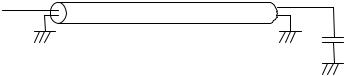
3)Output load.
Z=50W
Output 
50pF (External Load)
4)The access time is defined at 1.5V.
5)If tT is longer than 1ns, then the reference level for timing of input signals is VIH and VIL.
9/30
 Loading...