


OKI MSM51V8221A-40JS, MSM51V8221A-40ZS, MSM51V8221A-30ZS, MSM51V8221A-40GS-K, MSM51V8221A-30GS-K Datasheet
...E2L0054-28-Z2
This version: Dec. 1998
¡SemiconductorSemiconductor MSM51V8221A
Previous version: Mar. 1998
MSM51V8221A
262,214-Word ´ 8-Bit Field Memory
DESCRIPTION
The OKI MSM51V8221A is a high performance 2-Mbit, 256K ´ 8-bit, Field Memory. It is designed for high-speed serial access applications such as HDTVs, conventional NTSC TVs, VTRs, digital movies and Multi-media systems. It is a FRAM for wide or low end use as general commodity TVs and VTRs, exclusively. The MSM51V8221A is not designed for the other use or high end use in medical systems, professional graphics systems which require long term picture, and data storage systems and others. The 2-Mbit capacity fits one field of a conventional NTSC TV screen.
Each of the 8-bit planes has separate serial write and read ports. These employ independent control clocks to support asynchronous read and write operations. Different clock rates are also supported, which allow alternate data rates between write and read data streams.
The MSM51V8221A provides high speed FIFO, First-In First-Out, operation without external refreshing: it refreshes its DRAM storage cells automatically, so that it appears fully static to the users. Moreover, fully static type memory cells and decoders for serial access enable the refresh free serial access operation, so that serial read and/or write control clock can be halted high or low for any duration as long as the power is on. Internal conflicts of memory access and refreshing operations are prevented by special arbitration logic.
TheMSM51V8221A'sfunctionissimple,andsimilartoadigitaldelaydevicewhosedelay-bit-length is easily set by reset timing. The delay length, and the number of read delay clocks between write and read, is determined by externally controlled write and read reset timings.
Additional SRAM serial registers, or line buffers for the initial access of 256 ´8-bit enable high speed first-bit-access with no clock delay just after the write or read reset timings.
The MSM51V8221A is similar in operation and functionality to OKI 1-Mbit Field Memory MSM51V4221C. It has a write mask function or input enable function (IE), and read-data skipping function or output enable function (OE). The differences between write enable (WE) and input enable (IE), and between read enable (RE) and output enable (OE) are that WE and RE can stop serial write/readaddressincrements,butIEandOEcannotstoptheincrement,whenwrite/readclocking is continuously applied to MSM51V8221A. The input enable (IE) function allows the user to write intoselectedlocationsofthememoryonly,leavingtherestofthememorycontentsunchanged. This facilitates data processing to display a "picture in picture" on a TV screen.
1/16
¡ Semiconductor |
MSM51V8221A |
FEATURES
•Single power supply : 3.3 V ±0.3 V
•512 Rows ´ 512 Columns ´ 8 bits
•Fast FIFO (First-In First-Out) operation
•High speed asynchronous serial access
Read/write cycle time |
30 ns/40 ns |
Access time |
30 ns/35 ns |
•Functional compatibility with OKI MSM51V4221C
•Write mask function (Input enable control)
•Data skipping function (Output enable control)
•Self refresh (No refresh control is required)
•Package options :
28-pin 400 mil plastic ZIP |
(ZIP28-P-400-1.27) |
(Product : MSM51V8221A-xxZS) |
||||
28-pin 400 mil plastic SOJ |
(SOJ28-P-400-1.27) |
(Product : MSM51V8221A-xxJS) |
||||
28-pin 430 mil plastic SOP |
(SOP28-P-430-1.27-K) (Product : MSM51V8221A-xxGS-K) |
|||||
|
|
|
|
|
xx indicates speed rank. |
|
PRODUCT FAMILY |
|
|
|
|
|
|
|
|
|
|
|
||
Family |
|
Access Time (Max.) |
Cycle Time (Min.) |
Package |
||
|
|
|
|
|
|
|
MSM51V8221A-30ZS |
|
30 ns |
|
30 ns |
|
400 mil 28-pin ZIP |
MSM51V8221A-40ZS |
|
35 ns |
|
40 ns |
|
|
|
|
|
|
|||
|
|
|
|
|
|
|
MSM51V8221A-30JS |
|
30 ns |
|
30 ns |
|
400 mil 28-pin SOJ |
MSM51V8221A-40JS |
|
35 ns |
|
40 ns |
|
|
|
|
|
|
|||
|
|
|
|
|
|
|
MSM51V8221A-30GS-K |
|
30 ns |
|
30 ns |
|
430 mil 28-pin SOP |
|
|
|
|
|
|
|
MSM51V8221A-40GS-K |
|
35 ns |
|
40 ns |
|
|
|
|
|
|
|||
2/16

¡ Semiconductor |
MSM51V8221A |
PIN CONFIGURATION (TOP VIEW)
WE |
1 |
IE |
|
DIN4 |
1 |
28 |
VCC |
|
DIN4 |
1 |
28 |
VCC |
||
|
2 |
|
DIN5 |
2 |
27 |
DIN3 |
|
|||||||
DIN0 |
3 |
|
|
|
DIN5 |
2 |
27 |
DIN3 |
||||||
DIN2 |
4 |
DIN1 |
|
DIN6 |
3 |
26 |
DIN2 |
|
DIN6 |
3 |
26 |
DIN2 |
||
5 |
DIN3 |
|
|
|
|
|
|
|
|
|||||
VCC |
6 |
|
DIN7 |
4 |
25 |
DIN1 |
|
DIN7 |
4 |
25 |
DIN1 |
|||
7 |
DIN4 |
RSTW |
5 |
24 |
DIN0 |
|
RSTW |
5 |
24 |
DIN0 |
||||
|
8 |
|
||||||||||||
DIN5 |
9 |
DIN6 |
SWCK |
6 |
23 |
IE |
|
SWCK |
6 |
23 |
IE |
|||
|
10 |
|
NC |
7 |
22 |
WE |
|
NC |
7 |
22 |
WE |
|||
DIN7 |
11 |
|
|
|
||||||||||
RSTW |
|
RE |
8 |
21 |
NC |
|
||||||||
SWCK |
12 |
|
|
RE |
8 |
21 |
NC |
|||||||
13 |
|
|
|
|
|
|
|
|
|
|||||
NC |
|
OE |
9 |
20 |
SRCK |
OE |
9 |
20 |
SRCK |
|||||
NC |
14 |
|
||||||||||||
15 |
RE |
DOUT7 |
10 |
19 |
RSTR |
DOUT7 10 |
19 |
RSTR |
||||||
|
16 |
DOUT6 11 |
18 |
DOUT0 |
||||||||||
OE |
17 |
DOUT7 |
DOUT6 11 |
18 |
DOUT0 |
|||||||||
DOUT6 |
18 |
DOUT5 12 |
17 |
DOUT1 |
DOUT5 12 |
17 |
DOUT1 |
|||||||
19 |
|
|||||||||||||
DOUT5 |
D |
|
4 |
13 |
16 |
D |
|
2 |
||||||
|
20 |
OUT |
OUT |
DOUT4 13 |
16 |
DOUT2 |
||||||||
DOUT4 |
21 |
|
|
|
|
|
|
|
||||||
VSS |
|
VSS 14 |
15 |
DOUT3 |
VSS 14 |
15 |
DOUT3 |
|||||||
|
22 |
|
||||||||||||
DOUT3 |
23 |
|
|
DOUT2 |
|
|
|
24 |
|
|
|
||||
DOUT1 |
|
|
|
|
|||
25 |
|
|
28-Pin Plastic SOJ |
28-Pin Plastic SOP |
|||
|
|
||||||
RSTR |
|
26 |
DOUT0 |
|
|
|
|
|
|
|
|
||||
27 |
|
|
SRCK |
|
|
|
|
28 |
|
|
|
||||
|
|
|
|
|
|||
|
|
|
|
|
|||
|
|
|
|
|
|
|
|
28-Pin Plastic ZIP
Pin Name |
Function |
SWCK |
Serial Write Clock |
|
|
SRCK |
Serial Read Clock |
|
|
WE |
Write Enable |
|
|
RE |
Read Enable |
|
|
IE |
Input Enable |
|
|
OE |
Output Enable |
|
|
RSTW |
Write Reset Clock |
|
|
RSTR |
Read Reset Clock |
|
|
DIN0 - 7 |
Data Input |
DOUT0 - 7 |
Data Output |
VCC |
Power Supply (3.3 V) |
VSS |
Ground (0 V) |
NC |
No Connection |
|
|
3/16
4/16
DOUT (´ 8) |
OE |
RE |
|
RSTR |
SRCK |
|||||||||||
|
|
|
|
|
|
|
|
|
|
|
|
|
|
|
|
|
|
|
|
|
|
|
|
|
|
|
|
|
|
|
|
|
|
|
|
|
|
|
|
|
|
|
|
|
|
|
|
|
|
|
Data-out |
|
|
Serial |
Read |
|
|
|
Controller |
|
|||||||
|
|
|
|
|
|
|||||||||||
Buffer (´ 8) |
|
|
|
|
|
|
|
|
|
|
|
|
|
|||
|
|
|
|
|
|
|
|
|
|
|
|
|
||||
|
|
|
|
|
|
|
|
|
|
|
|
|
|
|
|
|
|
|
|
|
|
|
|
|
|
|
|
|
|
|
|
|
|
|
|
|
|
|
|
|
|
|
|
|
|
|
|
|
|
|
|
|
|
|
|
|
|
512-Word Serial Read Register (´ 8) |
|
||||||||
|
|
|
|
|
|
|
|
|
|
|
|
|
|
|
||
|
|
|
|
|
|
Read Line Buffer |
|
|
Read Line Buffer |
|
||||||
|
|
|
|
|
|
Low-Half (´ 8) |
|
|
High-Half (´ 8) |
|
||||||
|
|
|
|
|
|
|
|
|
|
|
|
|
|
|
|
|
|
|
|
|
|
|
|
|
256 (´ 8) |
|
|
256 (´ 8) |
|||||
|
|
|
|
|
|
|
|
|
|
|
|
|
|
|
|
|
|
71-Word |
|
|
|
|
|
|
|
|
|
|
|
|
|||
Sub-Register (´ 8) |
|
|
|
|
|
|
|
|
|
|
|
X |
||||
|
|
|
|
|
|
|
|
|
256K (´ 8) |
|
|
|||||
|
|
|
|
|
|
|
|
|
|
|
||||||
|
|
|
|
|
|
|
|
|
Memory |
|
|
|
|
Decoder |
||
|
|
|
|
|
|
|
|
|
|
Array |
|
|
|
|
|
|
|
|
|
|
|
|
|
|
|
|
|
|
|
|
|
||
71-Word |
|
|
|
|
Sub-Register (´ 8) |
|
|
|
|
|
|
256 (´ 8) |
256 (´ 8) |
|
|
Write Line Buffer |
Write Line Buffer |
||
|
Low-Half (´ 8) |
High-Half (´ 8) |
||
|
512-Word Serial Write Register (´ 8) |
|||
Data-in |
|
|
|
|
Buffer (´ 8) |
Serial |
Write |
Controller |
|
DIN (´ 8) |
IE |
WE |
RSTW |
SWCK |
Read/Write
and Refresh
Controller
Clock
Oscillator
VBB
Generator
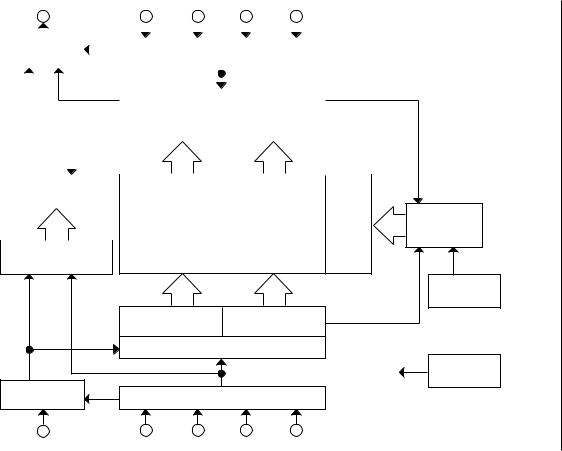
DIAGRAM BLOCK |
Semiconductor ¡ |
MSM51V8221A
¡ Semiconductor |
MSM51V8221A |
OPERATION
Write Operation
The write operation is controlled by three clocks, SWCK, RSTW, and WE. Write operation is accomplished by cycling SWCK, and holding WE high after the write address pointer reset operation or RSTW.
Each write operation, which begins after RSTW, must contain at least 80 active write cycles, i.e. SWCK cycles while WE is high. To transfer the last data to the DRAM array, which at that time is stored in the serial data registers attached to the DRAM array, an RSTW operation is required after the last SWCK cycle.
Write Reset : RSTW
The first positive transition of SWCK after RSTW becomes high resets the write address counters to zero. RSTW setup and hold times are referenced to the rising edge of SWCK. Because the write reset function is solely controlled by the SWCK rising edge after the high level of RSTW, the states of WE and IE are ignored in the write reset cycle.
Before RSTW may be brought high again for a further reset operation, it must be low for at least two SWCK cycles.
Data Inputs : DIN0 - 7
Write Clock : SWCK
The SWCK latches the input data on chip when WE is high, and also increments the internal write addresspointer. Data-insetuptimetDS,andholdtimetDH arereferencedtotherisingedgeofSWCK.
Write Enable : WE
WEis used for data write enable/disablecontrol. WEhighlevelenables theinput,and WElowlevel disables the input and holds the internal write address pointer. There are no WE disable time (low) andWEenabletime(high)restrictions,becausetheMSM51V8221Aisinfullystaticoperationaslong as the power is on. Note that WE setup and hold times are referenced to the rising edge of SWCK.
Input Enable : IE
IE is used to enable/disable writing into memory. IE high level enables writing. The internal write addresspointerisalwaysincrementedbycyclingSWCKregardlessoftheIElevel. NotethatIEsetup and hold times are referenced to the rising edge of SWCK.
5/16
¡ Semiconductor |
MSM51V8221A |
Read Operation
The read operation is controlled by three clocks, SRCK, RSTR, and RE. Read operation is accomplished by cycling SRCK, and holding RE high after the read address pointer reset operation or RSTR.
Each read operation, which begins after RSTR, must contain at least 80 active read cycles, i.e. SRCK cycles while RE is high.
Read Reset : RSTR
The first positive transition of SRCK after RSTR becomes high resets the read address counters to zero. RSTR setup and hold times are referenced to the rising edge of SRCK. Because the read reset function is solely controlled by the SRCK rising edge after the high level of RSTR, the states of RE and OE are ignored in the read reset cycle.
Before RSTR may be brought high again for a further reset operation, it must be low for at least two SRCK cycles.
Data Out : DOUT0 - 7
Read Clock : SRCK
Data is shifted out of the data registers. It is triggered by the rising edge of SRCK when RE is high during a read operation. The SRCK input increments the internal read address pointer when RE is high.
The three-state output buffer provides direct TTL compatibility (no pullup resistor required). Data out is the same polarity as data in. The output becomes valid after the access time interval tAC that begins with the rising edge of SRCK. There are no output valid time restrictions on MSM51V8221A.
Read Enable : RE
The function of RE is to gate of the SRCK clock for incrementing the read pointer. When RE is high before the rising edge of SRCK, the read pointer is incremented. When RE is low, the read pointer
is not incremented. RE setup times (tRENS and tRDSS) and RE hold times (tRENH and tRDSH) are referenced to the rising edge of the SRCK clock.
Output Enable : OE
OE is used to enable/disable the outputs. OE high level enables the outputs. The internal read address pointer is always incremented by cycling SRCK regardless of the OE level. Note that OE setup and hold times are referenced to the rising edge of SRCK.
6/16
 Loading...