


OKI MSM51V18165F-70TS-K, MSM51V18165F-70TS-L, MSM51V18165F-70JS, MSM51V18165F-50TS-K, MSM51V18165F-50TS-L Datasheet
... Semiconductor
This version:Oct.1999
MSM51V18165F
1,048,576-Word x 16-Bit DYNAMIC RAM : FAST PAGE MODE TYPE WITH EDO
DESCRIPTION
The MSM51V18165F is a 1,048,576-word ´ 16-bit dynamic RAM fabricated in Oki’s silicon-gate CMOS technology. The MSM51V18165F achieves high integration, high-speed operation, and low-power consumption because Oki manufactures the device in a quadruple-layer polysilicon/double-layer metal CMOS process. The MSM51V18165F is available in a 42-pin plastic SOJ or 50/44-pin plastic TSOP.
FEATURES
·1,048,576-word ´ 16-bit configuration
·Single 3.3V power supply, ±0.3V tolerance
· |
Input |
: LVTTL compatible, low input capacitance |
· |
Output |
: LVTTL compatible, 3-state |
· |
Refresh |
: 1024 cycles/16ms |
·Fast page mode with EDO, read modify write capability
·CAS before RAS refresh, hidden refresh, RAS-only refresh capability
·CAS before RAS self-refresh capability
·Package options:
42-pin 400mil plastic SOJ |
(SOJ42-P-400-1.27) |
(Product : MSM51V18165F-xxJS) |
50/44-pin 400mil plastic TSOP |
(TSOPII50/44-P-400-0.80-K) |
(Product : MSM51V18165F-xxTS-K) |
|
(TSOPII50/44-P-400-0.80-L) |
(Product : MSM51V18165F-xxTS-L) |
|
|
xx indicates speed rank. |
PRODUCT FAMILY
Family |
|
Access Time (Max.) |
|
Cycle Time |
Power Dissipation |
||||
tRAC |
|
tAA |
tCAC |
|
tOEA |
(Min.) |
Operating (Max.) |
Standby (Max.) |
|
|
|
|
|||||||
|
50ns |
|
25ns |
13ns |
|
13ns |
84ns |
324mW |
|
|
|
|
|
|
|
|
|
|
|
MSM51V18165F |
60ns |
|
30ns |
15ns |
|
15ns |
104ns |
288mW |
1.8mW |
|
|
|
|
|
|
|
|
|
|
|
70ns |
|
35ns |
20ns |
|
20ns |
124ns |
252mW |
|
|
|
|
|
|
|
|
|
|
|
No.
1/14

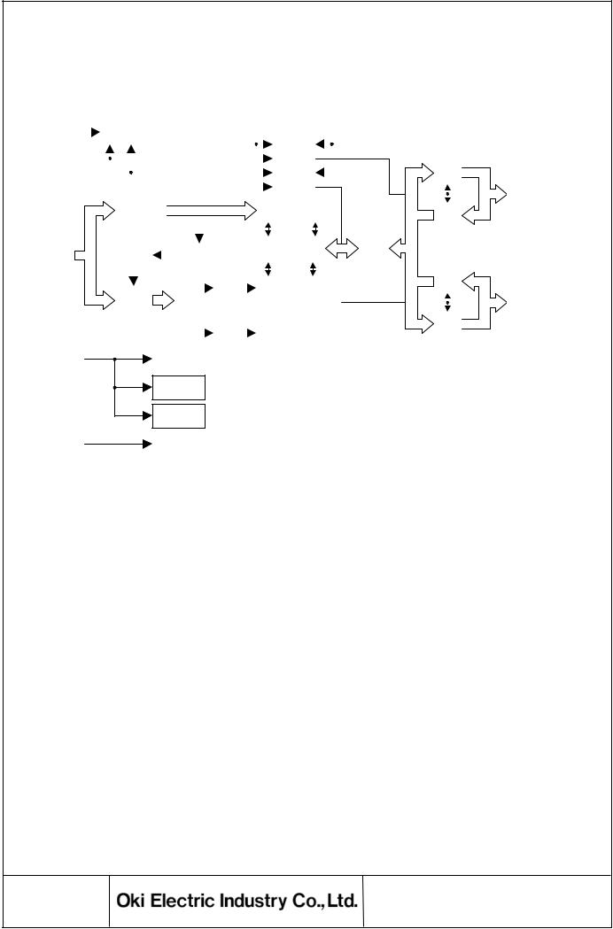
PIN CONFIGRATION (TOP VIEW)
VCC 1 |
42 |
VSS |
DQ1 2 |
41 |
DQ16 |
DQ2 3 |
40 |
DQ15 |
DQ3 4 |
39 |
DQ14 |
DQ4 5 |
38 |
DQ13 |
VCC 6 |
37 |
VSS |
DQ5 7 |
36 |
DQ12 |
DQ6 8 |
35 |
DQ11 |
DQ7 9 |
34 |
DQ10 |
DQ8 10 |
33 |
DQ9 |
NC 11 |
32 |
NC |
NC 12 |
31 |
LCAS |
WE 13 |
30 UCAS |
|
RAS 14 |
29 |
OE |
NC 15 |
28 |
A9 |
NC 16 |
27 |
A8 |
A0 17 |
26 |
A7 |
A1 18 |
25 |
A6 |
A2 19 |
24 |
A5 |
A3 20 |
23 |
A4 |
VCC 21 |
22 |
VSS |
42-Pin Plastic SOJ
VCC |
1 |
|
50 |
VSS |
VSS |
50 |
|
1 |
VCC |
|
|
|
|
|
|
|
|
|
|
DQ1 |
2 |
|
49 |
DQ16 DQ16 |
49 |
|
2 |
DQ1 |
|
|
|
|
|
|
|
|
|
|
|
DQ2 |
3 |
|
48 |
DQ15 DQ15 |
48 |
|
3 |
DQ2 |
|
|
|
|
|
|
|
|
|
|
|
DQ3 |
4 |
|
47 |
DQ14 DQ14 |
47 |
|
4 |
DQ3 |
|
|
|
|
|
|
|
|
|
|
|
DQ4 |
5 |
|
46 |
DQ13 DQ13 |
46 |
|
5 |
DQ4 |
|
|
|
|
|
|
|
|
|
|
|
VCC |
6 |
|
45 |
VSS |
VSS |
45 |
|
6 |
VCC |
|
|
|
|
|
|
|
|
|
|
DQ5 |
7 |
|
44 |
DQ12 DQ12 |
44 |
|
7 |
DQ5 |
|
|
|
|
|
|
|
|
|
|
|
DQ6 |
8 |
|
43 |
DQ11 DQ11 |
43 |
|
8 |
DQ6 |
|
|
|
|
|
|
|
|
|
|
|
DQ7 |
9 |
|
42 |
DQ10 DQ10 |
42 |
|
9 |
DQ7 |
|
|
|
|
|
|
|
|
|
|
|
DQ8 |
10 |
|
41 |
DQ9 |
DQ9 |
41 |
|
10 |
DQ8 |
|
|
|
|
NC |
NC |
|
|
|
|
NC |
11 |
|
40 |
40 |
|
11 |
NC |
||
|
|
NC |
15 |
|
|
36 |
|
NC |
|
|
|
NC |
36 |
|
|
15 |
|
NC |
||||||||
|
|
|
|
|
|
|
|
|
|
|
|
|
|
|
|
|
|
|
|
|
|
|
|
|||
|
|
NC |
16 |
|
|
35 |
|
LCAS |
|
|
LCAS |
|
35 |
|
|
16 |
|
NC |
||||||||
|
|
|
|
|
|
|
|
|
|
|
|
|
|
|
|
|
|
|
|
|
|
|||||
|
|
WE |
|
17 |
|
|
34 |
|
UCAS |
|
UCAS |
|
34 |
|
|
|
17 |
|
WE |
|
|
|||||
|
|
|
|
|
|
|
|
|
|
|
|
|
|
|
|
|
|
|
|
|
|
|
|
|||
|
RAS |
|
18 |
|
|
33 |
|
OE |
|
|
|
|
OE |
|
33 |
|
|
18 |
|
RAS |
|
|||||
|
|
|
|
|
|
|
|
|
|
|
|
|
|
|
|
|
|
|
|
|
|
|
|
|||
|
|
NC |
19 |
|
|
32 |
|
A9 |
|
|
|
A9 |
32 |
|
|
19 |
|
NC |
||||||||
|
|
|
|
|
|
|
|
|
|
|
|
|
|
|
|
|
|
|
|
|
|
|
|
|||
|
|
NC |
20 |
|
|
31 |
|
A8 |
|
|
|
A8 |
31 |
|
|
20 |
|
NC |
||||||||
|
|
|
|
|
|
|
|
|
|
|
|
|
|
|
|
|
|
|
|
|
|
|
|
|||
|
|
A0 |
21 |
|
|
30 |
|
A7 |
|
|
|
A7 |
30 |
|
|
21 |
|
A0 |
||||||||
|
|
|
|
|
|
|
|
|
|
|
|
|
|
|
|
|
|
|
|
|
|
|
||||
|
|
A1 22 |
|
29 |
|
A6 |
|
|
|
A6 29 |
|
22 |
|
A1 |
||||||||||||
|
|
|
|
|
|
|
A5 |
|
|
|
|
|
|
|
|
|
|
|
A2 |
|||||||
|
|
A2 23 |
|
28 |
|
|
|
|
A5 28 |
|
23 |
|
||||||||||||||
|
|
|
|
|
|
|
A4 |
|
|
|
|
|
|
|
|
|
|
A3 |
||||||||
|
|
A3 24 |
|
27 |
|
|
|
|
A4 27 |
|
|
24 |
||||||||||||||
|
|
|
|
|
|
|
|
|
|
|
|
|
|
|
|
|
|
|
|
|
|
|
||||
|
|
VCC 25 |
|
26 |
|
VSS |
|
|
VSS 26 |
|
25 |
|
VCC |
|||||||||||||
|
|
|
|
|
|
|
|
|
|
|
|
|
|
|
|
|
|
|
|
|
|
|
|
|
|
|
|
|
|
|
55/44-Pin Plastic TSOP |
|
|
|
|
|
55/44-Pin Plastic TSOP |
|
|
|
|||||||||||||
|
|
|
|
|
|
|
(K Type) |
|
|
|
|
|
|
|
|
|
|
|
(L Type) |
|
|
|
||||
Pin Name |
Function |
|
|
A0–A9 |
Address Input |
|
|
RAS |
Row Address Strobe |
|
|
LCAS |
Lower Byte Column Address Strobe |
|
|
UCAS |
Upper Byte Column Address Strobe |
|
|
DQ1–DQ16 |
Data Input/Data Output |
|
|
OE |
Output Enable |
|
|
WE |
Write Enable |
|
|
VCC |
Power Supply (3.3V) |
VSS |
Ground (0V) |
NC |
No Connection |
|
|
Note : The same power supply voltage must be provided to every VCC pin, and the same
GND voltage level must be provided to every VSS pin.
No.
2/14
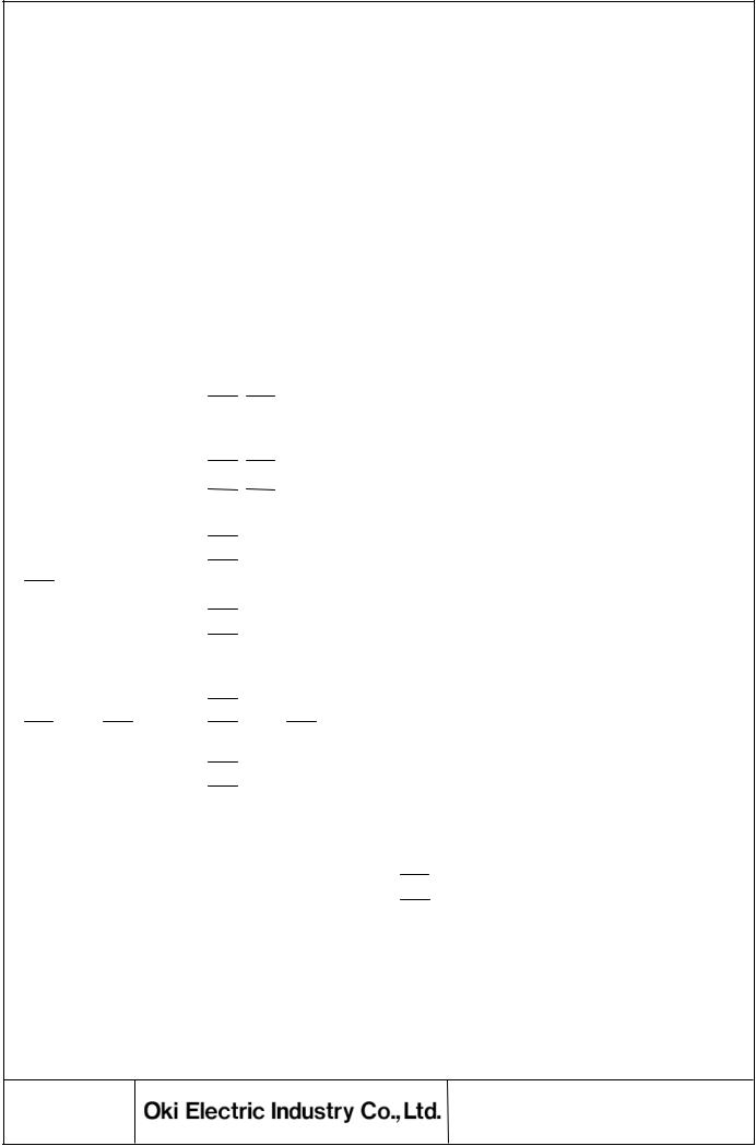
BLOCK DIAGRAM
|
|
|
|
|
|
|
|
|
|
|
|
|
|
|
|
|
|
|
|
|
|
|
|
|
|
|
|
|
|
|
|
|
|
|
|
|
|
|
|
|
|
|
|
|
|
|
|
|
|
|
|
|
|
|
|
|
|
|
|
|
|
|
WE |
OE |
|
|
|
|
|
|
|
||||||||
|
|
|
|
|
|
|
Timing |
|
|
|
|
|
|
|
|
|
|
|
|
|
|
|
|
|
|
|
|
|
|
|
|
|
|
|
|
||||
|
RAS |
|
|
|
|
|
|
|
|
|
|
|
|
|
|
|
|
|
|
|
|
|
|
|
|
|
|
|
|
|
|
|
|||||||
|
|
|
Generator |
|
|
|
|
|
|
|
|
|
|
|
|
|
|
|
|
|
|
|
|
|
|
|
|
|
|
|
|
||||||||
|
|
|
|
|
|
|
|
|
|
|
|
|
|
|
|
|
|
|
|
|
|
|
|
|
|
I/O |
|
|
|
|
|
|
|
|
|
|
|
|
|
|
|
|
|
|
|
|
|
|
|
|
|
|
|
|
|
|
|
|
|
|
|
|
|
|
|
|
|
|
|
|
|
|
|
|
|
|
|
|
|
|
|
|
|
|
|
|
|
|
|
|
|
|
|
|
|
|
|
|
|
|
|
|
|
Controller |
|
|
|
|
|
|
|
|
|
|
|
|
|
||
|
LCAS |
|
|
|
|
|
|
|
|
|
|
|
|
|
|
|
|
|
|
|
|
|
|
|
|
|
|
|
|
|
|
|
|
|
|
|
|
||
|
|
|
|
|
|
|
|
|
|
|
|
|
|
|
|
|
|
|
|
|
|
|
|
|
|
|
|
|
|
|
|
||||||||
|
|
|
|
|
|
|
|
|
|
|
|
|
|
|
|
|
|
|
|
|
|
|
|
|
|
|
|
|
|
|
|
|
|
|
|
Output |
|
||
UCAS |
|
|
|
|
|
|
|
|
|
|
|
|
|
|
|
|
|
|
|
|
|
|
I/O |
|
|
|
|
|
|
|
8 |
Buffers |
8 |
||||||
|
|
|
|
|
|
|
|
|
|
|
|
|
|
|
|
|
|
|
|
|
|
|
|
|
|
Controller |
|
|
|
|
|
|
|
|
|
|
|||
|
|
|
|
|
|
|
|
|
|
|
|
|
|
|
|
|
|
|
|
|
|
|
|
|
|
|
|
|
|
|
|
|
|
|
|
|
|
DQ1-DQ8 |
|
|
|
|
|
|
|
|
|
|
|
|
|
|
|
|
|
|
|
|
|
|
|
|
|
|
|
|
|
|
|
|
|
|
|
|
|
|
|
||
|
|
|
|
|
|
|
|
|
|
|
|
|
|
|
|
|
|
|
|
|
|
|
|
|
|
|
|
|
|
|
|
|
|
|
|
|
|
|
|
|
|
|
|
|
|
|
|
|
Column |
|
|
|
|
|
|
|
|
|
|
|
|
|
|
|
|
|
|
|
|
|
|
|
|
|
|
|
|||
|
|
|
|
10 |
|
|
Address |
|
|
|
|
|
|
10 |
|
Column Decoders |
|
|
|
|
|
8 |
Input |
8 |
|||||||||||||||
|
|
|
|
|
|
|
|
|
Buffers |
|
|
|
|
|
|
|
|
|
|
|
|
|
|
|
|
|
|
|
|
|
Buffers |
||||||||
|
|
|
|
|
|
|
|
|
|
|
|
|
|
|
|
|
|
|
|
|
|
|
|
|
|
|
|
|
|
|
|
|
|||||||
|
|
|
|
|
|
|
|
|
|
|
|
|
|
|
|
|
|
|
|
|
|
|
|
|
|
|
|
|
|
|
|
|
|
|
|
|
|
|
|
|
|
|
|
|
|
|
|
|
|
|
|
|
|
|
|
|
|
|
|
|
|
|
|
|
|
|
|
|
|
|
|
|
|
|
|
|
|
|
|
|
|
|
|
|
|
|
|
|
|
|
|
|
|
|
|
|
|
|
|
|
|
|
|
|
|
|
|
|
|
|
|
|
|
|
|
|
|
|
|
|
|
|
|
|
|
|
|
|
|
|
|
|
|
|
|
|
|
|
|
|
|
|
|
|
|
|
|
|
|
|
|
|
I/O |
|
|
|
|
|
|
A0-A9 |
|
|
|
|
|
Internal |
|
|
|
Refresh |
|
|
|
|
|
Sense Amplifiers |
16 |
Selector |
16 |
|
|
|
|
|
|||||||||||||||
|
|
|
|
|
Address |
|
|
|
Control Clock |
|
|
|
|
|
|
|
|
|
|
|
|
|
|
|
|
|
|
|
|||||||||||
|
|
|
|
|
|
|
|
|
Counter |
|
|
|
|
|
|
|
|
|
|
|
|
|
|
|
|
|
|
|
|
|
|
|
|||||||
|
|
|
|
|
|
|
|
|
|
|
|
|
|
|
|
|
|
|
|
|
|
|
|
|
|
|
|
|
|
|
|
|
|
|
|
||||
|
|
|
|
|
|
|
|
|
|
|
|
|
|
|
|
|
|
|
|
|
|
|
|
|
|
|
|
|
|
|
|
|
|
|
|
|
|
|
|
|
|
|
|
|
|
|
|
|
|
|
|
|
|
|
|
|
|
|
|
|
|
|
|
|
|
|
|
|
|
|
|
|
|
8 |
Input |
8 |
|||
|
|
|
|
|
|
|
|
|
|
|
|
|
|
|
|
|
|
|
|
|
|
|
|
|
|
|
|
|
|
|
|
|
|
Buffers |
|||||
|
|
|
|
10 |
|
|
Row |
10 |
|
Row |
|
|
|
|
|
|
|
|
|
|
|
|
|
|
|
|
|
|
|
|
|
|
|
||||||
|
|
|
|
|
|
Address |
|
|
|
|
|
|
|
|
|
|
|
|
|
|
|
|
|
|
|
|
|
|
|
DQ9-DQ16 |
|||||||||
|
|
|
|
|
|
|
|
|
Buffers |
|
|
|
Deco- |
|
|
Word |
|
|
|
|
|
Memory |
|
|
|
|
|
|
|
|
|
|
|
||||||
|
|
|
|
|
|
|
|
|
|
|
|
ders |
|
|
Drivers |
|
|
|
|
|
Cells |
|
|
|
|
|
|
|
|
|
|
|
|||||||
|
|
|
|
|
|
|
|
|
|
|
|
|
|
|
|
|
|
|
|
|
|
|
|
|
|
|
|
8 |
Output |
8 |
|||||||||
|
|
|
|
|
|
|
|
|
|
|
|
|
|
|
|
|
|
|
|
|
|
|
|
|
|
|
|
|
|
|
|
|
|
||||||
|
|
|
|
|
|
|
|
|
|
|
|
|
|
|
|
|
|
|
|
|
|
|
|
|
|
|
|
|
|
|
|
|
|
Buffers |
|||||
|
|
|
|
|
|
|
|
|
|
|
|
|
|
|
|
|
|
|
|
|
|
|
|
|
|
|
|
|
|
|
|
|
|
|
|
|
|||
|
|
|
|
|
|
|
|
|
|
|
|
|
|
|
|
|
|
|
|
|
|
|
|
|
|
|
|
|
|
|
|
|
|
|
|
|
|
|
|
|
|
|
|
|
|
|
|
|
|
|
|
|
|
|
|
|
|
|
|
|
|
|
|
|
|
|
|
|
|
|
|
|
|
|
|
|
|
|
|
VCC
VSS
On Chip
VBB Generator
On Chip
IVCC Generator
FUNCTION TABLE
|
|
|
|
|
|
Input Pin |
|
|
|
|
|
DQ Pin |
Function Mode |
||||
|
|
|
|
|
|
|
|
|
|
|
|
|
|
|
|
|
|
|
RAS |
|
|
LCAS |
|
|
UCAS |
|
|
WE |
|
|
OE |
|
DQ1-DQ8 |
DQ9-DQ16 |
|
|
|
|
|
|
|
|
|
|
|
|
|
|
|
|
|
|
|
|
H |
* |
|
* |
|
|
* |
|
* |
|
High-Z |
High-Z |
Standby |
||||
|
|
|
|
|
|
|
|
|
|
|
|
|
|
|
|
|
|
|
L |
|
H |
|
H |
|
* |
|
* |
|
High-Z |
High-Z |
Refresh |
||||
|
|
|
|
|
|
|
|
|
|
|
|
|
|
|
|
|
|
|
L |
|
L |
|
H |
|
H |
|
L |
DOUT |
High-Z |
Lower Byte Read |
|||||
|
L |
|
H |
|
L |
|
H |
|
L |
High-Z |
DOUT |
Upper Byte Read |
|||||
|
L |
|
L |
|
L |
|
H |
|
L |
DOUT |
DOUT |
Word Read |
|||||
|
L |
|
L |
|
H |
|
L |
|
H |
DIN |
Don’t Care |
Lower Byte Write |
|||||
|
L |
|
H |
|
L |
|
L |
|
H |
Don’t Care |
DIN |
Upper Byte Write |
|||||
|
L |
|
L |
|
L |
|
L |
|
H |
DIN |
DIN |
Word Write |
|||||
|
L |
|
L |
|
L |
|
H |
|
H |
High-Z |
High-Z |
¾ |
|||||
|
|
|
|
|
|
|
|
|
|
|
|
|
|
|
|
|
|
* : “H” or “L”
No.
3/14
ELECTRICAL CHARACTERISTICS
Absolute Maximum Ratings
Parameter |
Symbol |
Rating |
Unit |
|
|
|
|
Voltage on Any Pin Relative to VSS |
VIN, VOUT |
- 0.5 to VCC + 0.3 |
V |
Voltage VCC Supply relative to VSS |
VCC |
- 0.5 to 4.6 |
V |
Short Circuit Output Current |
IOS |
50 |
mA |
Power Dissipation |
PD* |
1 |
W |
Operating Temperature |
Topr |
0 to 70 |
°C |
Storage Temperature |
Tstg |
- 55 to 150 |
°C |
*: Ta = 25°C
Recommended Operating Conditions
(Ta = 0 °C to 70 °C)
Parameter |
Symbol |
Min. |
Typ. |
Max. |
Unit |
|
|
|
|
|
|
|
|
Power Supply Voltage |
VCC |
3.0 |
3.3 |
3.6 |
V |
|
VSS |
0 |
0 |
0 |
V |
||
|
||||||
Input High Voltage |
VIH |
2.0 |
¾ |
VCC + 0.3*1 |
V |
|
Input Low Voltage |
VIL |
- 0.3*2 |
¾ |
0.8 |
V |
Notes: *1. The input voltage is VCC + 1.0V when the pulse width is less than 20ns (the pulse width is with respect to the point at which VCC is applied).
*2. The input voltage is VSS - 1.0V when the pulse width is less than 20ns (the pulse width respect to the point at which VSS is applied).
Capacitance
(VCC = 3.3V ± 0.3V, Ta = 25°C, f=1MHz)
|
|
|
|
|
Parameter |
Symbol |
Typ. |
Max. |
Unit |
||||||
|
|
|
|
|
|
|
|
|
|
|
|
|
|
|
|
Input Capacitance (A0 - A9) |
CIN1 |
¾ |
5 |
pF |
|||||||||||
Input Capacitance |
CIN2 |
¾ |
7 |
pF |
|||||||||||
|
|
|
|
|
|
|
|
|
|
|
|||||
(RAS, LCAS, UCAS, WE, OE) |
|||||||||||||||
|
|
|
|
||||||||||||
|
|
|
|
|
|
|
|
|
|
|
|
|
|
|
|
Output Capacitance (DQ1 - DQ16) |
CI/O |
¾ |
7 |
pF |
|||||||||||
No.
4/14
DC Characteristics
(VCC = 3.3V ± 0.3V, Ta = 0°C to 70°C)
|
|
|
MSM51V18165 |
MSM51V18165 |
MSM51V18165 |
|
|
||||
Parameter |
Symbol |
Condition |
F-50 |
F-60 |
F-70 |
Unit |
Note |
||||
|
|
|
|
|
|
||||||
|
|
|
|
|
|
|
|
|
|
|
|
|
|
|
Min. |
Max. |
Min. |
Max. |
Min. |
Max. |
|
|
|
|
|
|
|
|
|
|
|
|
|
|
|
Output High Voltage |
VOH |
IOH = -2.0mA |
2.4 |
VCC |
2.4 |
VCC |
2.4 |
VCC |
V |
|
|
Output Low Voltage |
VOL |
IOL = 2mA |
0 |
0.4 |
0 |
0.4 |
0 |
0.4 |
V |
|
|
Input Leakage |
|
0V £ VI £ VCC+0.3V; |
|
|
|
|
|
|
|
|
|
ILI |
All other pins not |
- 10 |
10 |
- 10 |
10 |
- 10 |
10 |
mA |
|
||
Current |
|
||||||||||
|
|
under test = 0V |
|
|
|
|
|
|
|
|
|
|
|
|
|
|
|
|
|
|
|
|
|
Output Leakage |
ILO |
DQ disable |
- 10 |
10 |
- 10 |
10 |
- 10 |
10 |
mA |
|
|
|
|
||||||||||
Current |
0V £ VO £ VCC |
|
|||||||||
|
|
|
|
|
|
|
|
|
|||
Average Power |
|
RAS, CAS cycling, |
|
|
|
|
|
|
|
|
|
Supply Current |
ICC1 |
¾ |
90 |
¾ |
80 |
¾ |
70 |
mA |
1,2 |
||
tRC = Min. |
|||||||||||
(Operating) |
|
|
|
|
|
|
|
|
|
||
|
|
|
|
|
|
|
|
|
|
||
|
|
|
|
|
|
|
|
|
|
|
|
Power Supply |
|
RAS, CAS = VIH |
¾ |
2 |
¾ |
2 |
¾ |
2 |
|
|
|
Current |
ICC2 |
RAS, CAS |
¾ |
0.5 |
¾ |
0.5 |
¾ |
0.5 |
mA |
1 |
|
(Standby) |
|
³ VCC - 0.2V |
|
|
|||||||
|
|
|
|
|
|
|
|
|
|||
Average Power |
|
RAS cycling, |
|
|
|
|
|
|
|
|
|
|
|
|
|
|
|
|
|
|
|
||
Supply Current |
ICC3 |
CAS = VIH, |
¾ |
90 |
¾ |
80 |
¾ |
70 |
mA |
1,2 |
|
(RAS-only Refresh) |
|
tRC = Min. |
|
|
|
|
|
|
|
|
|
Power Supply |
|
RAS = VIH, |
|
|
|
|
|
|
|
|
|
Current |
ICC5 |
CAS = VIL, |
¾ |
5 |
¾ |
5 |
¾ |
5 |
mA |
1 |
|
(Standby) |
|
DQ = enable |
|
|
|
|
|
|
|
|
|
|
|
|
|
|
|
|
|
|
|
||
|
|
|
|
|
|
|
|
|
|
|
|
Average Power |
|
RAS = cycling, |
|
|
|
|
|
|
|
|
|
Supply Current |
ICC6 |
¾ |
90 |
¾ |
80 |
¾ |
70 |
mA |
1,2 |
||
(CAS before RAS |
CAS before RAS |
||||||||||
|
|
|
|
|
|
|
|
|
|||
Refresh) |
|
|
|
|
|
|
|
|
|
|
|
|
|
|
|
|
|
|
|
|
|
|
|
Average Power |
|
RAS = VIL, |
|
|
|
|
|
|
|
|
|
Supply Current |
ICC7 |
CAS cycling, |
¾ |
90 |
¾ |
80 |
¾ |
70 |
mA |
1,3 |
|
(Fast Page Mode) |
|
tHPC = Min. |
|
|
|
|
|
|
|
|
|
Notes: 1. ICC Max. is specified as ICC for output open condition.
2.The address can be changed once or less while RAS = VIL.
3.The address can be changed once or less while CAS = VIH.
No.
5/14
 Loading...