


OKI MSM514256CL-50ZS, MSM514256CL-60JS, MSM514256CL-60RS, MSM514256CL-60ZS, MSM514256CL-50JS Datasheet
...E2G0010-17-41
This version: Jan. 1998
¡SemiconductorSemiconductor MSM514256C/CL
Previous version: May 1997
MSM514256C/CL
262,144-Word ´ 4-Bit DYNAMIC RAM : FAST PAGE MODE TYPE
DESCRIPTION
The MSM514256C/CL is a 262,144-word ´ 4-bit dynamic RAM fabricated in Oki's silicon-gate CMOS technology. The MSM514256C/CL achieves high integration, high-speed operation, and low-power consumption because Oki manufactures the device in a quadruple-layer polysilicon/single-layer metal CMOS process. The MSM514256C/CL is available in a 20-pin plastic DIP, 26/20-pin plastic SOJ, or 20-pin plastic ZIP. The MSM514256CL (the low-power version) is specially designed for lower-power applications.
FEATURES
•262,144-word ´ 4-bit configuration
•Single 5 V power supply, ±10% tolerance
• Input : TTL compatible, low input capacitance
•Output : TTL compatible, 3-state
•Refresh : 512 cycles/8 ms, 512 cycles/64 ms (L-version)
•Fast page mode, read modify write capability
•CAS before RAS refresh, hidden refresh, RAS-only refresh capability
•Package options:
20-pin 300 mil plastic DIP |
(DIP20-P-300-2.54-W1) |
(Product : MSM514256C/CL-xxRS) |
26/20-pin 300 mil plastic SOJ |
(SOJ26/20-P-300-1.27) |
(Product : MSM514256C/CL-xxJS) |
20-pin 400 mil plastic ZIP |
(ZIP20-P-400-1.27) |
(Product : MSM514256C/CL-xxZS) |
|
|
xx indicates speed rank. |
PRODUCT FAMILY
Family |
Access Time (Max.) |
Cycle Time |
Power Dissipation |
|||||
|
|
|
|
(Min.) |
|
|
||
tRAC |
tAA |
tCAC |
tOEA |
Operating (Max.) |
Standby (Max.) |
|||
|
||||||||
|
|
|||||||
MSM514256C/CL-45 |
45 ns |
24 ns |
14 ns |
14 ns |
90 ns |
468 mW |
|
|
|
|
|
|
|
|
|
|
|
MSM514256C/CL-50 |
50 ns |
26 ns |
14 ns |
14 ns |
100 ns |
446 mW |
5.5 mW/ |
|
|
|
|
|
|
|
|
|
|
MSM514256C/CL-60 |
60 ns |
30 ns |
15 ns |
15 ns |
120 ns |
385 mW |
1.1 mW (L-version) |
|
|
|
|
|
|
|
|
|
|
MSM514256C/CL-70 |
70 ns |
35 ns |
20 ns |
20 ns |
130 ns |
330 mW |
|
|
|
|
|
|
|
|
|
|
|
1/17
¡ Semiconductor |
MSM514256C/CL |
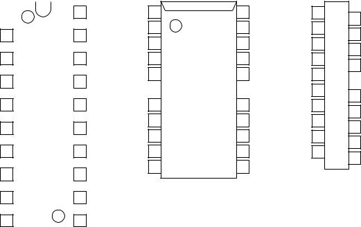
PIN CONFIGURATION (TOP VIEW)
|
|
|
20 |
|
DQ1 |
1 |
|
VSS |
|
DQ2 |
2 |
|
19 |
DQ4 |
WE 3 |
|
18 |
DQ3 |
|
RAS |
4 |
|
17 |
CAS |
NC |
5 |
|
16 |
OE |
A0 |
6 |
|
15 |
A8 |
A1 |
7 |
|
14 |
A7 |
A2 |
8 |
|
13 |
A6 |
A3 |
9 |
|
12 |
A5 |
VCC 10 |
|
11 |
A4 |
|
|
|
|
|
|
DQ1 |
1 |
26 |
VSS |
OE |
1 |
2 |
CAS |
|
DQ2 |
2 |
25 |
DQ4 |
DQ3 |
3 |
|||
4 |
DQ4 |
|||||||
WE 3 |
24 |
DQ3 |
VSS |
5 |
||||
6 |
DQ1 |
|||||||
RAS |
4 |
23 |
CAS |
DQ2 |
7 |
|||
8 |
WE |
|||||||
NC |
5 |
22 |
OE |
RAS |
9 |
|||
NO LEAD |
||||||||
|
|
|
|
A0 |
11 |
|||
|
|
|
|
12 |
A1 |
|||
A0 |
9 |
18 |
A8 |
A2 |
13 |
|||
14 |
A3 |
|||||||
A1 |
10 |
17 |
A7 |
VCC |
15 |
|||
16 |
A4 |
|||||||
A2 |
11 |
16 |
A6 |
A5 |
17 |
|||
18 |
A6 |
|||||||
A3 |
12 |
15 |
A5 |
A7 |
19 |
|||
20 |
A8 |
|||||||
VCC 13 |
14 |
A4 |
|
|
||||
|
|
|
|
|||||
|
26/20-Pin Plastic SOJ |
|
20-Pin Plastic ZIP |
|||||
|
|
|
|
|
|
|||
20-Pin Plastic DIP
Pin Name |
Function |
|
|
A0 - A8 |
Address Input |
|
|
RAS |
Row Address Strobe |
|
|
CAS |
Column Address Strobe |
|
|
DQ1 - DQ4 |
Data Input/Data Output |
|
|
OE |
Output Enable |
|
|
WE |
Write Enable |
|
|
VCC |
Power Supply (5 V) |
VSS |
Ground (0 V) |
NC |
No Connection |
|
|
2/17

¡ Semiconductor MSM514256C/CL
BLOCK DIAGRAM
|
RAS |
|
Timing |
|
|
|
|
|
|
|
Generator |
|
|
|
|
|
|
||
|
|
|
|
|
Timing |
|
|
||
|
|
|
|
|
|
|
|
|
|
CAS |
|
|
|
|
Generator |
|
|
||
|
Column |
|
|
|
|
|
Write |
|
|
9 |
|
|
9 |
Column |
|
Clock |
WE |
|
|
Address |
|
|
Decoders |
|
Generator |
|
OE |
||
|
Buffers |
|
|
|
|
|
|
|
|
|
|
|
|
|
|
|
|
|
|
|
|
|
|
|
|
|
4 |
Output |
4 |
|
|
|
|
|
|
|
Buffers |
||
|
Internal |
|
Refresh |
|
|
I/O |
|
||
A0 - A8 |
|
Sense |
|
|
|
||||
Address |
|
4 |
|
4 DQ1 - DQ4 |
|||||
|
Control Clock |
Amplifiers |
4 |
|
|||||
|
Counter |
|
|
Selector |
Input |
|
|||
|
|
|
|
|
|
|
|
||
|
|
|
|
|
|
|
4 |
4 |
|
|
|
|
|
|
|
|
Buffers |
||
|
|
|
|
|
|
|
|
|
|
|
Row |
|
Row |
|
|
|
|
|
|
9 |
Address 9 |
Word |
Memory |
|
|
|
|
||
|
Buffers |
|
De- |
|
|
|
|
||
|
|
Drivers |
Cells |
|
|
|
|
||
|
|
|
coders |
|
|
|
|
||
|
|
|
|
|
|
|
|
|
|
VCC
On Chip
VBB Generator
VSS
3/17

¡ Semiconductor MSM514256C/CL
ELECTRICAL CHARACTERISTICS
Absolute Maximum Ratings
|
Parameter |
Symbol |
|
Rating |
|
|
Unit |
|
|
|
|
|
|
|
|
|
Voltage on Any Pin Relative to VSS |
VT |
|
–1.0 to 7.0 |
|
|
V |
|
Short Circuit Output Current |
IOS |
|
50 |
|
|
mA |
|
Power Dissipation |
PD* |
|
1 |
|
|
W |
|
Operating Temperature |
Topr |
|
0 to 70 |
|
|
°C |
|
Storage Temperature |
Tstg |
|
–55 to 150 |
|
|
°C |
|
|
*: Ta = 25°C |
|
|
|
|
|
Recommended Operating Conditions |
|
|
|
(Ta = 0°C to 70°C) |
|||
|
|
|
|
|
|
||
|
|
|
|
|
|
|
|
|
Parameter |
Symbol |
Min. |
Typ. |
Max. |
|
Unit |
|
|
|
|
|
|
|
|
|
Power Supply Voltage |
VCC |
4.5 |
5.0 |
5.5 |
|
V |
|
VSS |
0 |
0 |
0 |
|
V |
|
|
|
|
|||||
|
Input High Voltage |
VIH |
2.4 |
— |
6.5 |
|
V |
|
Input Low Voltage |
VIL |
–1.0 |
— |
0.8 |
|
V |
Capacitance |
|
|
(VCC = 5 V ±10%, Ta = 25°C, f = 1 MHz) |
|||
|
|
|
|
|||
|
Parameter |
Symbol |
Typ. |
|
Max. |
Unit |
|
|
|
|
|
|
|
|
Input Capacitance (A0 - A8) |
CIN1 |
— |
|
5 |
pF |
|
Input Capacitance (RAS, CAS, WE, OE) |
CIN2 |
— |
|
5 |
pF |
|
Output Capacitance (DQ1 - DQ4) |
CI/O |
— |
|
6 |
pF |
4/17
¡ Semiconductor |
|
|
|
|
|
|
|
MSM514256C/CL |
|||||
DC Characteristics |
|
|
|
|
|
|
(VCC = 5 V ±10%, Ta = 0°C to 70°C) |
||||||
|
|
|
|
|
|
|
|||||||
|
|
|
MSM514256 |
MSM514256 |
MSM514256 |
MSM514256 |
|
|
|||||
Parameter |
Symbol |
Condition |
C/CL-45 |
C/CL-50 |
C/CL-60 |
C/CL-70 |
Unit |
Note |
|||||
|
|
|
|
|
|
|
|
|
|
|
|
|
|
|
|
|
Min. |
Max. |
Min. |
Max. |
Min. |
Max. |
Min. |
Max. |
|
|
|
|
|
|
|
|
|
|
|
|
|
|
|
|
|
Output High Voltage |
VOH |
IOH = –5.0 mA |
2.4 |
VCC |
2.4 |
VCC |
2.4 |
VCC |
2.4 |
VCC |
V |
|
|
Output Low Voltage |
VOL |
IOL = 4.2 mA |
0 |
0.4 |
0 |
0.4 |
0 |
0.4 |
0 |
0.4 |
V |
|
|
|
|
0 V £ VI £ 6.5 V; |
|
|
|
|
|
|
|
|
|
|
|
Input Leakage Current |
ILI |
All other pins not |
–10 |
10 |
–10 |
10 |
–10 |
10 |
–10 |
10 |
mA |
|
|
|
|
under test = 0 V |
|
|
|
|
|
|
|
|
|
|
|
|
|
|
|
|
|
|
|
|
|
|
|
|
|
Output Leakage Current |
ILO |
DQ disable |
–10 |
10 |
–10 |
10 |
–10 |
10 |
–10 |
10 |
mA |
|
|
0 V £ VO £ 5.5 V |
|
||||||||||||
|
|
|
|
|
|
|
|
|
|
|
|
||
Average Power |
|
RAS, CAS cycling, |
|
|
|
|
|
|
|
|
|
|
|
Supply Current |
ICC1 |
— |
85 |
— |
80 |
— |
70 |
— |
60 |
mA |
1, 2 |
||
tRC = Min. |
|||||||||||||
(Operating) |
|
|
|
|
|
|
|
|
|
|
|
||
|
|
|
|
|
|
|
|
|
|
|
|
||
|
|
|
|
|
|
|
|
|
|
|
|
|
|
Power Supply |
|
RAS, CAS = VIH |
— |
2 |
— |
2 |
— |
2 |
— |
2 |
mA |
1 |
|
ICC2 |
RAS, CAS |
— |
1 |
— |
1 |
— |
1 |
— |
1 |
||||
Current (Standby) |
|
|
|||||||||||
|
³ VCC –0.2 V |
— |
200 |
— |
200 |
— |
200 |
— |
200 |
mA |
1, 5 |
||
|
|
||||||||||||
Average Power |
|
RAS cycling, |
|
|
|
|
|
|
|
|
|
|
|
Supply Current |
ICC3 |
CAS = VIH, |
— |
85 |
— |
80 |
— |
70 |
— |
60 |
mA |
1, 2 |
|
(RAS-only Refresh) |
|
tRC = Min. |
|
|
|
|
|
|
|
|
|
|
|
Power Supply |
|
RAS = VIH, |
|
|
|
|
|
|
|
|
|
|
|
ICC5 |
CAS = VIL, |
— |
5 |
— |
5 |
— |
5 |
— |
5 |
mA |
1 |
||
Current (Standby) |
|||||||||||||
|
DQ = enable |
|
|
|
|
|
|
|
|
|
|
||
|
|
|
|
|
|
|
|
|
|
|
|
||
Average Power |
|
RAS cycling, |
|
|
|
|
|
|
|
|
|
|
|
Supply Current |
ICC6 |
— |
85 |
— |
80 |
— |
70 |
— |
60 |
mA |
1, 2 |
||
CAS before RAS |
|||||||||||||
(CAS before RAS Refresh) |
|
|
|
|
|
|
|
|
|
|
|
||
|
|
|
|
|
|
|
|
|
|
|
|
||
|
|
|
|
|
|
|
|
|
|
|
|
|
|
Average Power |
|
RAS = VIL, |
|
|
|
|
|
|
|
|
|
|
|
Supply Current |
ICC7 |
CAS cycling, |
— |
80 |
— |
75 |
— |
65 |
— |
55 |
mA |
1, 3 |
|
(Fast Page Mode) |
|
tPC = Min. |
|
|
|
|
|
|
|
|
|
|
|
Average Power |
|
tRC = 125 ms, |
|
|
|
|
|
|
|
|
|
1, 2, |
|
Supply Current |
ICC10 |
CAS before RAS, |
— |
300 |
— |
300 |
— |
300 |
— |
300 |
mA |
||
4, 5 |
|||||||||||||
(Battery Backup) |
|
tRAS £ 1 ms |
|
|
|
|
|
|
|
|
|
||
|
|
|
|
|
|
|
|
|
|
|
|||
Notes : 1. ICC Max. is specified as ICC for output open condition.
2.The address can be changed once or less while RAS = VIL.
3.The address can be changed once or less while CAS = VIH.
4.VCC – 0.2 V £ VIH £ 6.5 V, –1.0 V £ VIL £ 0.2 V.
5.L-version.
5/17
¡ Semiconductor |
|
|
|
|
|
|
|
MSM514256C/CL |
|
||||
AC Characteristics (1/2) |
|
|
|
|
|
|
|
|
|
|
|
|
|
|
|
|
|
(VCC = 5 V ±10%, Ta = 0°C to 70°C) Note 1, 2, 3, 4, 5 |
|
||||||||
|
|
|
MSM514256 |
MSM514256 |
MSM514256 |
MSM514256 |
|
|
|
||||
|
Parameter |
Symbol |
C/CL-45 |
C/CL-50 |
C/CL-60 |
C/CL-70 |
Unit |
Note |
|
||||
|
|
|
|
|
|
|
|
|
|
|
|
|
|
|
|
|
Min. |
Max. |
Min. |
Max. |
Min. |
Max. |
Min. |
Max. |
|
|
|
|
|
|
|
|
|
|
|
|
|
|
|
|
|
|
Random Read or Write Cycle Time |
tRC |
90 |
— |
100 |
— |
120 |
— |
130 |
— |
ns |
|
|
|
Read Modify Write Cycle Time |
tRWC |
140 |
— |
150 |
— |
170 |
— |
185 |
— |
ns |
|
|
|
Fast Page Mode Cycle Time |
tPC |
34 |
— |
36 |
— |
40 |
— |
45 |
— |
ns |
|
|
|
Fast Page Mode Read Modify Write |
tPRWC |
75 |
— |
77 |
— |
90 |
— |
95 |
— |
ns |
|
|
|
Cycle Time |
|
|
||||||||||
|
|
|
|
|
|
|
|
|
|
|
|
|
|
|
|
|
|
|
|
|
|
|
|
|
|
|
|
|
Access Time from RAS |
tRAC |
— |
45 |
— |
50 |
— |
60 |
— |
70 |
ns |
6, 7, 8 |
|
|
Access Time from CAS |
tCAC |
— |
14 |
— |
14 |
— |
15 |
— |
20 |
ns |
6, 7 |
|
|
Access Time from Column Address |
tAA |
— |
24 |
— |
26 |
— |
30 |
— |
35 |
ns |
6, 8 |
|
|
Access Time from CAS Precharge |
tCPA |
— |
28 |
— |
30 |
— |
35 |
— |
40 |
ns |
6 |
|
|
Access Time from OE |
tOEA |
— |
14 |
— |
14 |
— |
15 |
— |
20 |
ns |
6 |
|
|
Output Low Impedance Time from CAS |
tCLZ |
0 |
— |
0 |
— |
0 |
— |
0 |
— |
ns |
6 |
|
|
CAS to Data Output Buffer Turn-off Delay Time |
tOFF |
0 |
10 |
0 |
10 |
0 |
10 |
0 |
10 |
ns |
9 |
|
|
OE to Data Output Buffer Turn-off Delay Time |
tOEZ |
0 |
10 |
0 |
10 |
0 |
10 |
0 |
10 |
ns |
9 |
|
|
Transition Time |
tT |
3 |
50 |
3 |
50 |
3 |
50 |
3 |
50 |
ns |
3 |
|
|
Refresh Period |
tREF |
— |
8 |
— |
8 |
— |
8 |
— |
8 |
ms |
|
|
|
Refresh Period (L-version) |
tREF |
— |
64 |
— |
64 |
— |
64 |
— |
64 |
ms |
|
|
|
RAS Precharge Time |
tRP |
35 |
— |
40 |
— |
50 |
— |
50 |
— |
ns |
|
|
|
RAS Pulse Width |
tRAS |
45 |
10,000 |
50 |
10,000 |
60 |
10,000 |
70 |
10,000 |
ns |
|
|
|
RAS Pulse Width (Fast Page Mode) |
tRASP |
45 |
100,000 |
50 |
100,000 |
60 |
100,000 |
70 |
100,000 |
ns |
|
|
|
RAS Hold Time |
tRSH |
14 |
— |
14 |
— |
15 |
— |
20 |
— |
ns |
|
|
|
RAS Hold Time referenced to OE |
tROH |
10 |
— |
10 |
— |
10 |
— |
10 |
— |
ns |
|
|
|
CAS Precharge Time (Fast Page Mode) |
tCP |
10 |
— |
10 |
— |
10 |
— |
10 |
— |
ns |
|
|
|
CAS Pulse Width |
tCAS |
14 |
10,000 |
14 |
10,000 |
15 |
10,000 |
20 |
10,000 |
ns |
|
|
|
CAS Hold Time |
tCSH |
45 |
— |
50 |
— |
60 |
— |
70 |
— |
ns |
|
|
|
CAS to RAS Precharge Time |
tCRP |
5 |
— |
5 |
— |
5 |
— |
5 |
— |
ns |
|
|
|
RAS Hold Time from CAS Precharge |
tRHCP |
28 |
— |
30 |
— |
35 |
— |
40 |
— |
ns |
|
|
|
RAS to CAS Delay Time |
tRCD |
17 |
31 |
18 |
36 |
20 |
45 |
20 |
50 |
ns |
7 |
|
|
RAS to Column Address Delay Time |
tRAD |
12 |
21 |
13 |
24 |
15 |
30 |
15 |
35 |
ns |
8 |
|
|
Row Address Set-up Time |
tASR |
0 |
— |
0 |
— |
0 |
— |
0 |
— |
ns |
|
|
|
Row Address Hold Time |
tRAH |
7 |
— |
8 |
— |
10 |
— |
10 |
— |
ns |
|
|
|
Column Address Set-up Time |
tASC |
0 |
— |
0 |
— |
0 |
— |
0 |
— |
ns |
|
|
|
Column Address Hold Time |
tCAH |
12 |
— |
13 |
— |
15 |
— |
15 |
— |
ns |
|
|
|
Column Address Hold Time from RAS |
tAR |
35 |
— |
40 |
— |
50 |
— |
55 |
— |
ns |
|
|
|
Column Address to RAS Lead Time |
tRAL |
24 |
— |
26 |
— |
30 |
— |
35 |
— |
ns |
|
|
6/17
 Loading...