


August 1986
Revised March 2000
DM74LS126A
Quad 3-STATE Buffer
General Description
This device contains four independent gates each of which performs a non-inverting buffer function. The outputs have the 3-STATE feature. When enabled, the outputs exhibit the low impedance characteristics of a standard LS output with additional drive capability to permit the driving of bus lines without external resistors. When disabled, both the output transistors are turned OFF presenting a high-imped- ance state to the bus line. Thus the output will act neither as a significant load nor as a driver. To minimize the possibility that two outputs will attempt to take a common bus to opposite logic levels, the disable time is shorter than the enable time of the outputs.
Ordering Code:
Order Number |
Package Number |
Package Description |
|
|
|
DM74LS126AM |
M14A |
14-Lead Small Outline Integrated Circuit (SOIC), JEDEC MS-120, 0.150 Narrow |
|
|
|
DM74LS126AN |
N14A |
14-Lead Plastic Dual-In-Line Package (PDIP), JEDEC MS-001, 0.300 Wide |
|
|
|
Devices also available in Tape and Reel. Specify by appending the suffix letter “X” to the ordering code.
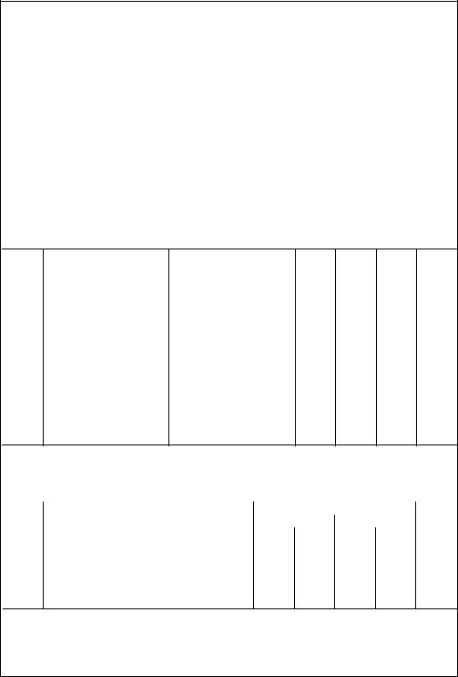
Connection Diagram |
Function Table |
|
|
||
|
|
|
|
Y = A |
|
|
|
|
|
|
|
|
|
Inputs |
|
Output |
|
|
|
|
|
|
|
|
|
A |
|
C |
Y |
|
|
|
|
|
|
|
|
L |
|
H |
L |
|
|
H |
|
H |
H |
|
|
X |
|
L |
Hi-Z |
|
|
|
|
|
|
H = HIGH Logic Level
L = LOW Logic Level
X = Either LOW or HIGH Logic Level
Hi-Z = 3-STATE (Outputs are disabled)
Buffer STATE-3 Quad DM74LS126A
© 2000 Fairchild Semiconductor Corporation |
DS006388 |
www.fairchildsemi.com |
DM74LS126A
Absolute Maximum Ratings(Note 1)
Supply Voltage |
7V |
Note 1: The “Absolute Maximum Ratings” are those values beyond which |
|
the safety of the device cannot be guaranteed. The device should not be |
|||
Input Voltage |
7V |
operated at these limits. The parametric values defined in the Electrical |
|
Characteristics tables are not guaranteed at the absolute maximum ratings. |
|||
Operating Free Air Temperature Range |
0°C to +70°C |
||
The “Recommended Operating Conditions” table will define the conditions |
|||
Storage Temperature Range |
−65°C to +150°C |
for actual device operation. |
|
|
Recommended Operating Conditions
Symbol |
Parameter |
Min |
Nom |
Max |
Units |
|
|
|
|
|
|
VCC |
Supply Voltage |
4.75 |
5 |
5.25 |
V |
VIH |
HIGH Level Input Voltage |
|
|
|
V |
VIL |
LOW Level Input Voltage |
|
|
0.8 |
V |
IOH |
HIGH Level Output Current |
|
|
−2.6 |
mA |
IOL |
LOW Level Output Current |
|
|
24 |
mA |
TA |
Free Air Operating Temperature |
0 |
|
70 |
°C |
Electrical Characteristics
over recommended operating free air temperature range (unless otherwise noted)
Symbol |
Parameter |
Conditions |
Typ |
Max |
Units |
Min |
|||||
|
|
|
(Note 2) |
|
|
|
|
|
|
|
|
VI |
Input Clamp Voltage |
VCC = Min, II = −18 mA |
|
−1.5 |
V |
VOH |
HIGH Level |
VCC = Min, IOH = Max |
2.4 |
|
V |
|
Output Voltage |
VIH = Min |
|
||
|
|
|
|
||
VOL |
LOW Level |
VCC = Min, IOL = Max |
0.35 |
0.5 |
|
|
Output Voltage |
VIL = Max, VIH = Min |
V |
||
|
|
|
|||
|
|
IOL = 12 mA, VCC = Min |
0.25 |
0.4 |
|
II |
Input Current @ Max Input Voltage |
VCC = Max, VI = 7V |
|
0.1 |
mA |
IIH |
HIGH Level Input Current |
VCC = Max, VI = 2.7V |
|
20 |
μA |
IIL |
LOW Level Input Current |
VCC = Max, VI = 0.4V |
|
−0.4 |
mA |
IOZH |
Off-State Output Current with |
VCC = Max, VO = 2.4V |
|
20 |
μA |
|
HIGH Level Output Voltage Applied |
VIH = Min, VIL = Max |
|
||
|
|
|
|
||
IOZL |
Off-State Output Current with |
VCC = Max, VO = 0.4V |
|
−20 |
μA |
|
LOW Level Output Voltage Applied |
VIH = Min, VIL = Max |
|
||
|
|
|
|
||
IOS |
Short Circuit Output Current |
VCC = Max (Note 3) |
−20 |
−100 |
mA |
ICC |
Supply Current |
VCC = Max |
12 |
22 |
mA |
Note 2: All typicals are at VCC = 5V, TA = 25°C.
Note 3: Not more than one output should be shorted at a time, and the duration should not exceed one second.
Switching Characteristics
VCC = 5V, TA = 25°C
|
|
|
RL = 667Ω |
|
|
|
Symbol |
Parameter |
CL = 50 pF |
CL = 150 pF |
Units |
||
|
|
Min |
Max |
Min |
Max |
|
|
|
|
|
|
|
|
tPLH |
Propagation Delay Time LOW-to-HIGH Level Output |
|
15 |
|
21 |
ns |
tPHL |
Propagation Delay Time HIGH-to-LOW Level Output |
|
18 |
|
22 |
ns |
tPZH |
Output Enable Time to HIGH Level Output |
|
30 |
|
36 |
ns |
tPZL |
Output Enable Time to LOW Level Output |
|
30 |
|
42 |
ns |
tPHZ |
Output Disable Time from HIGH Level Output (Note 4) |
|
25 |
|
|
ns |
tPLZ |
Output Disable Time from LOW Level Output (Note 4) |
|
25 |
|
|
ns |
Note 4: CL = 5pF.
www.fairchildsemi.com |
2 |
 Loading...