


Fairchild Semiconductor DM74LS123SJX, DM74LS123SJ, DM74LS123N, DM74LS123MX, DM74LS123M Datasheet
...August 1986
Revised April 2000
DM74LS123
Dual Retriggerable One-Shot
with Clear and Complementary Outputs
General Description
The DM74LS123 is a dual retriggerable monostable multivibrator capable of generating output pulses from a few nano-seconds to extremely long duration up to 100% duty cycle. Each device has three inputs permitting the choice of either leading edge or trailing edge triggering. Pin (A) is an active-LOW transition trigger input and pin (B) is an activeHIGH transition trigger input. The clear (CLR) input terminates the output pulse at a predetermined time independent of the timing components. The clear input also serves as a trigger input when it is pulsed with a low level pulse transition ( ). To obtain the best trouble free operation from this device please read the operating rules as well as the Fairchild Semiconductor one-shot application notes carefully and observe recommendations.
Features
■DC triggered from active-HIGH transition or active-LOW transition inputs
■Retriggerable to 100% duty cycle
■Compensated for VCC and temperature variations
■Triggerable from CLEAR input
■DTL, TTL compatible
■Input clamp diodes
Ordering Code:
Order Number |
Package Number |
Package Description |
|
|
|
DM74LS123M |
M16A |
16-Lead Small Outline Integrated Circuit (SOIC), JEDEC MS-012, 0.150 Narrow |
|
|
|
DM74LS123SJ |
M16D |
16-Lead Small Outline Package (SOP), EIAJ TYPE II, 5.3mm Wide |
|
|
|
DM74LS123N |
N16E |
16-Lead Plastic Dual-In-Line Package (PDIP), JEDEC MS-001, 0.300 Wide |
|
|
|
Devices also available in Tape and Reel. Specify by appending the suffix letter “X” to the ordering code.
Connection Diagram |
Function Table |
|
|
|
|
|
|||
|
|
|
|
|
|
||||
|
|
Inputs |
|
Outputs |
|||||
|
|
|
|
|
|
|
|
||
|
|
CLEAR |
|
A |
B |
Q |
Q |
||
|
|
|
|
|
|
|
|
|
|
|
|
L |
|
X |
X |
L |
|
H |
|
|
|
X |
|
H |
X |
L |
|
H |
|
|
|
X |
|
X |
L |
L |
|
H |
|
|
|
H |
|
L |
↑ |
|
|
||
|
|
H |
|
↓ |
H |
|
|
||
|
|
↑ |
|
L |
H |
|
|
||
|
|
|
|
|
|
|
|
|
|
|
H = HIGH Logic Level |
|
|
|
|
|
|
||
|
L = LOW Logic Level |
|
|
|
|
|
|
||
|
X = Can Be Either LOW or HIGH |
|
|
|
|
|
|||
|
↑ = Positive Going Transition |
|
|
|
|
|
|||
|
↓ = Negative Going Transition |
|
|
|
|
|
|||
|
= A Positive Pulse |
|
|
|
|
|
|
||
|
= A Negative Pulse |
|
|
|
|
|
|
||
Outputs Complementary and Clear with Shot-One Retriggerable Dual DM74LS123
© 2000 Fairchild Semiconductor Corporation |
DS006386 |
www.fairchildsemi.com |

DM74LS123
Functional Description
The basic output pulse width is determined by selection of an external resistor (RX) and capacitor (CX). Once triggered, the basic pulse width may be extended by retriggering the gated active-LOW transition or active-HIGH transition inputs or be reduced by use of the active-LOW or
Operating Rules
1.An external resistor (RX) and an external capacitor (CX) are required for proper operation. The value of CX may vary from 0 to any necessary value. For small time constants high-grade mica, glass, polypropylene, polycarbonate, or polystyrene material capacitors may be used. For large time constants use tantalum or special aluminum capacitors. If the timing capacitors have leakages approaching 100 nA or if stray capacitance from either terminal to ground is greater than 50 pF the timing equations may not represent the pulse width the device generates.
2.When an electrolytic capacitor is used for CX a switching diode is often required for standard TTL one-shots to prevent high inverse leakage current. This switching diode is not needed for the DM74LS123 one-shot and should not be used. In general the use of the switching diode is not recommended with retriggerable operation.
Furthermore, if a polarized timing capacitor is used on the DM74LS123 the negative terminal of the capacitor should be connected to the “CEXT” pin of the device (Figure 1).
FIGURE 1.
3.For CX >> 1000 pF the output pulse width (tW) is defined as follows:
tW = KRX CX where [RX is in kΩ ]
[CX is in pF]
[tW is in ns] K ≈ 0.37
4.The multiplicative factor K is plotted as a function of CX below for design considerations:
CLEAR input. Retriggering to 100% duty cycle is possible by application of an input pulse train whose cycle time is shorter than the output cycle time such that a continuous “HIGH” logic state is maintained at the “Q” output.
FIGURE 2.
5.For CX < 1000 pF see Figure 3 for tW vs. CX family curves with RX as a parameter:
FIGURE 3.
6.To obtain variable pulse widths by remote trimming, the following circuit is recommended:
FIGURE 4.
“Rremote” should be as close to the device pin as possible.
7.The retriggerable pulse width is calculated as shown below:
T = tW + tPLH = K × RX × CX + tPLH
The retriggered pulse width is equal to the pulse width plus a delay time period (Figure 5).
FIGURE 5.
www.fairchildsemi.com |
2 |
Operating Rules (Continued)
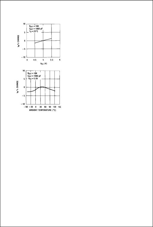
8.Output pulse width variation versus VCC and temperatures: Figure 6 depicts the relationship between pulse width variation versus VCC, and Figure 7 depicts pulse width variation versus temperatures.
FIGURE 6.
9.Under any operating condition CX and RX must be kept as close to the one-shot device pins as possible to minimize stray capacitance, to reduce noise pick-up, and to reduce I-R and Ldi/dt voltage developed along their connecting paths. If the lead length from CX to pins (6) and (7) or pins (14) and (15) is greater than 3 cm, for example, the output pulse width might be quite different from values predicted from the appropriate equations. A non-inductive and low capacitive path is necessary to ensure complete discharge of CX in each cycle of its operation so that the output pulse width will be accurate.
10.The CEXT pins of this device are internally connected to the internal ground. For optimum system performance they should be hard wired to the system’s return ground plane.
11.VCC and ground wiring should conform to good highfrequency standards and practices so that switching
transients on the VCC and ground return leads do not cause interaction between one-shots. A 0.01 F to 0.10F bypass capacitor (disk ceramic or monolithic type) from VCC to ground is necessary on each device. Fur-
thermore, the bypass capacitor should be located as close to the VCC-pin as space permits.
Note: For further detailed device characteristics and output performance please refer to the Fairchild Semiconductor one-shot application note AN-372.
FIGURE 7.
DM74LS123
3 |
www.fairchildsemi.com |
 Loading...