


Fairchild Semiconductor DM74ALS245AWMX, DM74ALS245AWM, DM74ALS245ASJX, DM74ALS245ASJ, DM74ALS245AN Datasheet
...
September 1986
Revised February 2000
DM74ALS245A
Octal 3-STATE Bus Transceiver
General Description
This advanced low power Schottky device contains 8 pairs of 3-STATE logic elements configured as octal bus transceivers. These circuits are designed for use in memory, microprocessor systems and in asynchronous bidirectional data buses. Two way communication between buses is controlled by the (DIR) input. Data transmits either from the A bus to the B bus or from the B bus to the A bus. Both the driver and receiver outputs can be disabled via the (G) enable input which causes outputs to enter the high impedance mode so that the buses are effectively isolated.
Features
■Advanced oxide-isolated, ion-implanted Schottky TTL process
■Non-inverting logic output
■Glitch free bus during power up and down
■3-STATE outputs independently controlled on A and B buses
■Low output impedance to drive terminated transmission lines to 133Ω
■Switching response specified into 500Ω/50 pF
■Specified to interface with CMOS at VOH = VCC − 2V
■PNP inputs to reduce input loading
■Switching specifications guaranteed over full temperature and VCC range
Ordering Code:
Order Number |
Package Number |
Package Description |
|
|
|
DM74ALS245AWM |
M20B |
20-Lead Small Outline Integrated Circuit (SOIC), JEDEC MS-013, 0.300 Wide |
|
|
|
DM74ALS245ASJ |
M20D |
20-Lead Small Outline Package (SOP), EIAJ TYPE II, 5.3mm Wide |
|
|
|
DM74ALS245AMSA |
MSA20 |
20-Lead Shrink Small Outline Package (SSOP), EIAJ TYPE II, 5.3mm Wide |
|
|
|
DM74ALS245AN |
N20A |
20-Lead Plastic Dual-In-Line Package (PDIP), JEDEC MS-001, 0.300 Wide |
|
|
|
Devices also available in Tape and Reel. Specify by appending the suffix letter “X” to the ordering code.
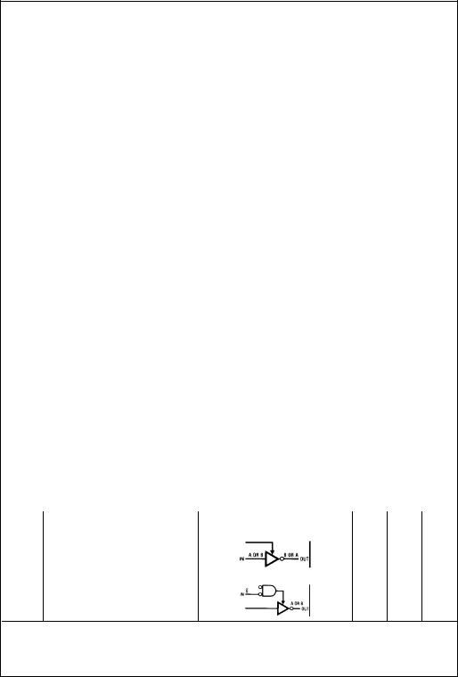
Connection Diagram |
Function Table |
|
|||||
|
|
|
|
|
|
|
|
|
|
|
|
Control |
|
||
|
|
|
|
Inputs |
|
Operation |
|
|
|
|
|
|
|
||
|
|
G |
|
DIR |
|
||
|
|
|
|
|
|
|
|
|
|
|
L |
|
L |
B Data to A Bus |
|
|
|
|
L |
|
H |
A Data to B Bus |
|
|
|
|
H |
|
X |
Hi-Z |
|
|
|
|
|
|
|
|
|
H = HIGH Logic Level
L = LOW Logic Level
X = Either HIGH or LOW Logic Level
Transceiver Bus STATE-3 Octal DM74ALS245A
© 2000 Fairchild Semiconductor Corporation |
DS006213 |
www.fairchildsemi.com |
DM74ALS245A
Absolute Maximum Ratings(Note 1)
Supply Voltage |
7V |
Input Voltage |
|
Control Inputs |
7V |
I/O Ports |
5.5V |
Operating Free Air Temperature Range |
0°C to +70°C |
Storage Temperature Range |
−65°C to +150°C |
Typical θJA |
|
N Package |
53.0°C/W |
M Package |
72.0°C/W |
Note 1: The “Absolute Maximum Ratings” are those values beyond which the safety of the device cannot be guaranteed. The device should not be operated at these limits. The parametric values defined in the Electrical Characteristics tables are not guaranteed at the absolute maximum ratings. The “Recommended Operating Conditions” table will define the conditions for actual device operation.
Recommended Operating Conditions
Symbol |
Parameter |
Min |
Typ |
Max |
Units |
|
|
|
|
|
|
VCC |
Supply Voltage |
4.5 |
5 |
5.5 |
V |
VIH |
HIGH Level Input Voltage |
2 |
|
|
V |
VIL |
LOW Level Input Voltage |
|
|
0.8 |
V |
IOH |
HIGH Level Output Current |
|
|
−15 |
mA |
IOL |
LOW Level Output Current |
|
|
24 |
mA |
TA |
Operating Free Air Temperature |
0 |
|
70 |
°C |
Electrical Characteristics
over recommended operating free air temperature range. All typical values are measured at VCC = 5V, TA = 25°C.
Symbol |
Parameter |
|
Conditions |
|
Min |
Typ |
Max |
Units |
|
|
|
|
|
|
|
|
|
VIK |
Input Clamp Voltage |
VCC = 4.5V, IIN = −18 mA |
|
|
|
−1.5 |
V |
|
VOH |
HIGH Level |
VCC = 4.5V, IOH = −3 mA |
|
2.4 |
3.2 |
|
V |
|
|
Output Voltage |
VCC = 4.5V, IOH = Max |
|
2 |
2.3 |
|
V |
|
|
|
IOH = −0.4 mA, VCC = 4.5V to 5.5V |
|
VCC − 2 |
|
|
V |
|
VOL |
LOW Level Output Voltage |
VCC = 4.5V |
IOL = 24 mA |
|
|
0.35 |
0.5 |
V |
II |
Input Current at Maximum |
VCC = 5.5V |
VIN = 7V |
Control Inputs |
|
|
0.1 |
mA |
|
Input Voltage |
|
VIN = 5.5V |
A or B Ports |
|
|
0.1 |
|
|
|
|
|
|
||||
IIH |
HIGH Level Input Current |
VCC = 5.5V, VIN = 2.7V |
|
|
|
20 |
μA |
|
IIL |
LOW Level Input Current |
VCC = 5.5V, VIN = 0.4V |
|
|
|
−0.1 |
mA |
|
IO |
Output Drive Current |
VCC = 5.5V, VOUT = 2.25V |
|
−30 |
|
−112 |
mA |
|
ICC |
Supply Current |
VCC = 5.5V |
Outputs HIGH |
|
|
30 |
45 |
mA |
|
|
|
Outputs LOW |
|
|
36 |
55 |
mA |
|
|
|
|
|
|
|
|
|
|
|
|
3-STATE |
|
|
38 |
58 |
mA |
|
|
|
|
|
|
|
|
|
Switching Characteristics |
(Note 2) |
|
|
|
||
over recommended operating free air temperature range |
|
|
|
|||
Symbol |
Parameter |
|
Circuit Configuration |
Min |
Max |
Units |
|
|
|
|
|
|
|
tPLH |
Propagation Delay Time |
|
|
3 |
10 |
ns |
|
LOW-to-HIGH Level Output |
|
|
|||
|
|
|
|
|
|
|
|
|
|
|
|
|
|
tPHL |
Propagation Delay Time |
|
|
3 |
10 |
ns |
|
HIGH-to-LOW Level Output |
|
|
|||
|
|
|
|
|
|
|
|
|
|
|
|
|
|
tPZL |
Output Enable Time to LOW Level |
|
|
5 |
20 |
ns |
tPZH |
Output Enable Time to HIGH Level |
|
|
5 |
20 |
ns |
tPLZ |
Output Disable Time from LOW Level |
|
|
4 |
15 |
ns |
tPHZ |
Output Disable Time from HIGH Level |
|
|
2 |
10 |
ns |
Note 2: Switching characteristic conditions are VCC = 4.5V to 5.5V, RL = 500Ω, CL = 50 pF.
www.fairchildsemi.com |
2 |
 Loading...