


 Loading...
Hardware Data Sheet
ET1100
Slave Controller
Section I – Technology
(Online at http://www.beckhoff.com)
Section II – Register Description
(Online at http://www.beckhoff.com)
Section III – Hardware Description
Pinout, Interface description, electrical and mechanical specification, ET1100 features and registers
Version 1.9
Date: 2014-07-07

DOCUMENT ORGANIZATION
DOCUMENT ORGANIZATION
The Beckhoff EtherCAT Slave Controller (ESC) documentation covers the following Beckhoff ESCs:
ET1200
ET1100
EtherCAT IP Core for Altera® FPGAs
EtherCAT IP Core for Xilinx® FPGAs
ESC20
The documentation is organized in three sections. Section I and section II are common for all Beckhoff ESCs, Section III is specific for each ESC variant.
The latest documentation is available at the Beckhoff homepage (http://www.beckhoff.com).
Section I – Technology (All ESCs)
Section I deals with the basic EtherCAT technology. Starting with the EtherCAT protocol itself, the frame processing inside EtherCAT slaves is described. The features and interfaces of the physical layer with its two alternatives Ethernet and EBUS are explained afterwards. Finally, the details of the functional units of an ESC like FMMU, SyncManager, Distributed Clocks, Slave Information Interface, Interrupts, Watchdogs, and so on, are described.
Since Section I is common for all Beckhoff ESCs, it might describe features which are not available in a specific ESC. Refer to the feature details overview in Section III of a specific ESC to find out which features are available.
Section II – Register Description (All ESCs)
Section II contains detailed information about all ESC registers. This section is also common for all Beckhoff ESCs, thus registers, register bits, or features are described which might not be available in a specific ESC. Refer to the register overview and to the feature details overview in Section III of a specific ESC to find out which registers and features are available.
Section III – Hardware Description (Specific ESC)
Section III is ESC specific and contains detailed information about the ESC features, implemented registers, configuration, interfaces, pinout, usage, electrical and mechanical specification, and so on. Especially the Process Data Interfaces (PDI) supported by the ESC are part of this section.
Additional Documentation
Application notes and utilities like pinout configuration tools for ET1100 can also be found at the Beckhoff homepage.
Trademarks
Beckhoff®, TwinCAT®, EtherCAT®, Safety over EtherCAT®, TwinSAFE® and XFC® are registered trademarks of and licensed by Beckhoff Automation GmbH. Other designations used in this publication may be trademarks whose use by third parties for their own purposes could violate the rights of the owners.
Patent Pending
The EtherCAT Technology is covered, including but not limited to the following German patent applications and patents: DE10304637, DE102004044764, DE102005009224, DE102007017835 with corresponding applications or registrations in various other countries.
Disclaimer
The documentation has been prepared with care. The products described are, however, constantly under development. For that reason the documentation is not in every case checked for consistency with performance data, standards or other characteristics. In the event that it contains technical or editorial errors, we retain the right to make alterations at any time and without warning. No claims for the modification of products that have already been supplied may be made on the basis of the data, diagrams and descriptions in this documentation.
Copyright
© Beckhoff Automation GmbH 07/2014.
The reproduction, distribution and utilization of this document as well as the communication of its contents to others without express authorization are prohibited. Offenders will be held liable for the payment of damages. All rights reserved in the event of the grant of a patent, utility model or design.
III-II |
Slave Controller – ET1100 Hardware Description |

DOCUMENT HISTORY
DOCUMENT HISTORY
Version Comment
0.6Editorial Changes
0.7Synchronous µController Interface LSB/MSB clarification table added
EEPROM_LOADED pull-down recommendation added
Chip label updated
VCCI/O/GNDI/O pins adjacent to LDO indicated
Frame processing order example corrected
I2C EEPROM interface description added
MII management interface description added
Corrected Process RAM size in Register Overview
P_CONF does not correspond with physical ports. See new port configuration tables for details.
Revision/Build information added
0.8CLK25OUT1/2 availability completed
Recommendations for unused input pins added (should not be left open)
EEPROM_SIZE description corrected from Kbyte to Kbit, possible EEPROM sizes range from 16 Kbit to 4 Mbit
RoHS compliance added
Autonegotiation is mandatory for ESCs
Description of power supply options added
Electrical characteristics added/revised
SPI_IRQ delay added, support for SPI masters with 2 or 4 bytes added
TX Shift timing diagram and description added
Internal 27 kΩ PU/PD resistors at EBUS-RX pins added
LED polarity depending on configuration pin setting described
Recommendation for voltage stabilization capacitors added
Description of Digital I/O behavior on watchdog expiration enhanced
8 bit asynchronous µController PDI connection added
EBUS ports are open failsafe
Reset example schematic added
Ethernet PHY requirements and PHY connection schematic added
MI_DATA pull-up requirement added
µController PDI: DATA bus signal direction corrected
Pin/Signal description overview added
PERR(x) LEDs are only for testing/debugging
Editorial changes
1.0RUN, LINKACT/x) and PERR(x) LED activity level corrected: active high if pulled down, active low if pulled up
DC Characteristics enhanced: added VReset Core, VID, VIC
Synchronous µController interface: timing characteristics enhanced
Note on RBIAS if no EBUS ports/only MII ports are used
DC SYNC/LATCH signal description and timing characteristics added
MII Interface chapter and MII timing characteristics added
EBUS Interface chapter added
Frame processing order, PHY requirements, EEPROM Interface description and MII Management Interface description moved to Section I
TX Shift description moved to MII Interface chapter
Ambient temperature range instead of junction temperature range
Editorial changes
Slave Controller – ET1100 Hardware Description |
III-III |

DOCUMENT HISTORY
Version Comment
1.1Port configurations with 2 ports: P_CONF[3] erroneously named P_MODE[3]
Clarified I/O voltage with respect to I/O power supply (only 3.3V I/O with VCCI/O=3.3V, and no 5V input tolerance unless VCCI/O=5V)
Update to ET1100 stepping 1
Added/revised OSC_IN, CLK25OUT1/2, and MII TX signal timings
Added soldering profile
PHY address configuration changed
Added feature detail overview, removed redundant feature details
PDI and DC SYNC/LATCH signals are not driven until EEPROM is loaded
Synchronous 8/16 bit µController interface: clarified that clock is CPU_CLK_IN
Editorial changes
1.2PHY address configuration chapter added, configuration revised
Enhanced link detection for MII available depending on PHY address configuration
Ethernet Management Interface: read and write times were interchanged
Reserved pins are input pins
Editorial changes
1.3Added reset timing figure and power-on value sample time
Distributed Clocks SYNC/LATCH signals are configurable and unidirectional
Information on CLK25OUT/CPU_CLK clock output during reset added
Description of internal PU/PD resistors at EBUS_RX pins enhanced
Added tDiff timing characteristic
Power supply example schematic clarified
Enhanced package information: MSL, ball’s material, and solder joint recommendation
Digital I/O PDI: added SOF/OUTVALID description, dispensable timings removed
Editorial changes
1.4Register 0x0980 is only available if DC Sync Unit is enabled (0x0140.10=1)
Updated solder joint recommendation
OSC_IN/OSC_OUT pin capacitance added, crystal connection note extended
Release Notes added
Timing requirement for asynchronous µController PDI (tADR_BHE_setup) relaxed
Input threshold voltage for OSC_IN added
Example schematic for transparent mode added
Renamed Err(x) LED to PERR(x)
Digital I/O PDI: OE_CONF functionality in bidirectional mode corrected
Digital I/O PDI: output event description corrected (EOF mode and WD_TRIG mode)
SPI PDI: access error if SPI_DI not 1 in the last read byte (not SPI_DO)
Async./sync. µC PDI: access error with A(0)=1 and nBHE=1 (not nBHE=0), timing requirements and diagrams clarified
Async. µC PDI: timing requirement for asynchronous µController PDI
(tADR_BHE_setup) relaxed
AC timing: forwarding delay figures enhanced
Editorial changes
1.5Reset timing figure corrected
Maximum soldering profile added
SPI PDI updated
SII EEPROM interface is a point-to-point connection
Editorial changes
1.6Update to ET1100-0002
Editorial changes
1.7µC PDI timing updated
Editorial changes
III-IV |
Slave Controller – ET1100 Hardware Description |

DOCUMENT HISTORY
Version Comment
1.8Enhanced Link Detection must not be activated if EBUS ports are used
Enhanced Link Detection for MII ports requires PHY address offset = 0
Digital Output principle schematic updated
Chip label updated
Editorial changes
1.9Update to ET1100-0003
Enhanced Link Detection for MII ports supports PHY address offset 0 and 16
Enhanced Link Detection for MII ports can be disabled at any time
Enhanced Link Detection for EBUS ports is always disabled
MII management interface issues additional MCLK cycle after write accesses
Remote link down signalling time configurable 0x0100[22]
Editorial changes
Slave Controller – ET1100 Hardware Description |
III-V |

CONTENTS
|
|
|
CONTENTS |
|
1 |
Overview |
|
|
1 |
|
1.1 |
Frame processing order |
2 |
|
|
1.2 |
Scope of this document |
3 |
|
|
1.3 |
Revision/Build History |
3 |
|
2 |
Features and Registers |
4 |
||
|
2.1 |
Features |
|
4 |
|
2.2 |
Registers |
|
7 |
3 |
Pin Description |
|
10 |
|
|
3.1 |
Overview |
|
10 |
|
|
3.1.1 |
Pin Overview |
10 |
|
|
3.1.2 |
Signal Overview |
12 |
|
|
3.1.3 |
PDI Signal Overview |
13 |
|
3.2 |
Configuration Pins |
14 |
|
|
|
3.2.1 |
Port Mode |
14 |
|
|
3.2.2 |
Port Configuration |
14 |
|
|
3.2.3 |
CPU_CLK MODE |
17 |
|
|
3.2.4 |
TX Shift |
17 |
|
|
3.2.5 |
CLK25OUT2 Enable |
17 |
|
|
3.2.6 |
Transparent Mode Enable |
18 |
|
|
3.2.7 |
Digital Control/Status Move |
19 |
|
|
3.2.8 |
PHY Address Offset |
19 |
|
|
3.2.9 |
Link Polarity |
19 |
|
|
3.2.10 |
SII EEPROM Size |
20 |
|
|
3.2.11 |
Reserved |
20 |
|
3.3 |
General ET1100 Pins |
21 |
|
|
3.4 |
SII EEPROM Interface Pins |
21 |
|
|
3.5 |
MII Management Pins |
22 |
|
|
3.6 |
Distributed Clocks SYNC/LATCH Pins |
22 |
|
|
3.7 |
LED Signals |
23 |
|
|
3.8 |
Physical Ports and PDI Pins |
24 |
|
|
|
3.8.1 |
Physical Port Signals |
25 |
|
|
3.8.2 |
MII Interface |
25 |
|
|
3.8.3 |
EBUS Interface |
26 |
|
|
3.8.4 |
PDI Pins |
26 |
|
|
3.8.5 |
Physical Port 0 |
27 |
|
|
3.8.6 |
Physical Port 1 |
28 |
|
|
3.8.7 |
Physical Port 2 / PDI byte 4 |
29 |
|
|
3.8.8 |
Physical Port 3 / PDI Bytes 2/3 |
30 |
|
|
3.8.9 |
PDI Bytes 0/1 |
31 |
|
|
|
|
|
III-VI |
|
|
Slave Controller – ET1100 Hardware Description |
|

|
|
|
|
CONTENTS |
|
3.9 |
PDI Signal Pinout depending on selected PDI |
32 |
|
|
|
3.9.1 |
Digital I/O Pin Out |
33 |
|
|
3.9.2 |
8/16 Bit asynchronous µController |
36 |
|
|
3.9.3 |
8/16 Bit synchronous µController |
37 |
|
|
3.9.4 |
SPI Pin Out |
38 |
|
3.10 |
Power Supply |
40 |
|
|
|
3.10.1 |
I/O Power Supply |
41 |
|
|
3.10.2 |
Logic Core Power Supply |
42 |
|
|
3.10.3 |
PLL Power Supply |
42 |
|
3.11 |
Reserved Pins |
42 |
|
4 |
MII Interface |
|
|
43 |
|
4.1 |
MII Interface Signals |
43 |
|
|
4.2 |
PHY Address Configuration |
44 |
|
|
4.3 |
TX Shift Compensation |
45 |
|
|
4.4 |
Timing specifications |
46 |
|
5 |
EBUS/LVDS Interface |
|
47 |
|
|
5.1 |
EBUS Interface Signals |
47 |
|
6 |
PDI description |
|
48 |
|
|
6.1 |
PDI Deactivated |
48 |
|
|
6.2 |
Digital I/O Interface |
49 |
|
|
|
6.2.1 |
Interface |
49 |
|
|
6.2.2 |
Configuration |
49 |
|
|
6.2.3 |
Digital Inputs |
50 |
|
|
6.2.4 |
Digital Outputs |
50 |
|
|
6.2.5 |
Bidirectional mode |
51 |
|
|
6.2.6 |
Output Enable/Output Configuration |
52 |
|
|
6.2.7 |
SyncManager Watchdog |
52 |
|
|
6.2.8 |
SOF |
53 |
|
|
6.2.9 |
OUTVALID |
53 |
|
|
6.2.10 |
EEPROM_LOADED |
53 |
|
|
6.2.11 |
Timing specifications |
53 |
|
6.3 |
SPI Slave Interface |
55 |
|
|
|
6.3.1 |
Interface |
55 |
|
|
6.3.2 |
Configuration |
55 |
|
|
6.3.3 |
SPI access |
55 |
|
|
6.3.4 |
Commands |
56 |
|
|
6.3.5 |
Address modes |
56 |
|
|
6.3.6 |
Interrupt request register (AL Event register) |
57 |
|
|
6.3.7 |
Write access |
57 |
|
|
6.3.8 |
Read access |
57 |
|
|
6.3.9 |
SPI access errors and SPI status flag |
59 |
|
|
|
||
|
Slave Controller – ET1100 Hardware Description |
III-VII |
||

CONTENTS
|
|
6.3.10 |
EEPROM_LOADED |
59 |
|
|
6.3.11 |
2 Byte and 4 Byte SPI Masters |
59 |
|
|
6.3.12 |
Timing specifications |
60 |
|
6.4 |
Asynchronous 8/16 bit µController Interface |
66 |
|
|
|
6.4.1 |
Interface |
66 |
|
|
6.4.2 |
Configuration |
66 |
|
|
6.4.3 |
µController access |
67 |
|
|
6.4.4 |
Write access |
67 |
|
|
6.4.5 |
Read access |
67 |
|
|
6.4.6 |
µController access errors |
68 |
|
|
6.4.7 |
EEPROM_LOADED |
68 |
|
|
6.4.8 |
Connection with 16 bit µControllers without byte addressing |
68 |
|
|
6.4.9 |
Connection with 8 bit µControllers |
69 |
|
|
6.4.10 |
Timing Specification |
70 |
|
6.5 |
Synchronous 8/16 bit µController Interface |
74 |
|
|
|
6.5.1 |
Interface |
74 |
|
|
6.5.2 |
Configuration |
74 |
|
|
6.5.3 |
µController access |
75 |
|
|
6.5.4 |
µController connection using Byte Select signals (BSn) |
76 |
|
|
6.5.5 |
µController connection using Transfer Size signals (SIZ) |
79 |
|
|
6.5.6 |
Write access |
81 |
|
|
6.5.7 |
Read access |
81 |
|
|
6.5.8 |
µController access errors |
81 |
|
|
6.5.9 |
EEPROM_LOADED |
81 |
|
|
6.5.10 |
Timing Specification |
82 |
7 |
Distributed Clocks SYNC/LATCH Signals |
86 |
||
|
7.1 |
Signals |
|
86 |
|
7.2 |
Timing specifications |
86 |
|
8 |
SII EEPROM Interface (I²C) |
87 |
||
|
8.1 |
Signals |
|
87 |
|
8.2 |
Timing specifications |
87 |
|
9 |
Example Schematics |
|
88 |
|
|
9.1 |
Clock source |
88 |
|
|
9.2 |
Power supply |
89 |
|
|
9.3 |
Dual purpose configuration input/LED output pins |
90 |
|
|
9.4 |
PHY Connection |
90 |
|
|
9.5 |
LVDS termination |
91 |
|
|
9.6 |
RBIAS resistor |
91 |
|
|
9.7 |
Reset Logic |
91 |
|
|
9.8 |
Transparent Mode |
92 |
|
10 |
Electrical Specifications and Timings |
93 |
||
|
|
|
|
|
III-VIII |
|
|
Slave Controller – ET1100 Hardware Description |
|

|
|
|
CONTENTS |
|
10.1 |
Absolute Maximum Ratings |
93 |
|
10.2 |
Electrical Characteristics |
93 |
11 |
Mechanical Specifications |
99 |
|
|
11.1 |
Package Information |
99 |
|
11.2 |
Tape and Reel Information |
101 |
|
11.3 |
Moisture Sensitivity and Storage |
102 |
|
11.4 |
Soldering Profile |
103 |
|
11.5 |
Ordering codes |
104 |
12 |
Appendix |
|
105 |
|
12.1 |
Support and Service |
105 |
|
|
12.1.1 Beckhoff’s branch offices and representatives |
105 |
|
12.2 |
Beckhoff Headquarters |
105 |
Slave Controller – ET1100 Hardware Description |
III-IX |

TABLES |
|
|
TABLES |
|
|
Table 1: ET1100 Main Features .............................................................................................................. |
|
1 |
Table 2: Frame Processing Order ........................................................................................................... |
|
2 |
Table 3: Revision/Build History................................................................................................................ |
|
3 |
Table 4: ET1100 Feature Details ............................................................................................................ |
|
4 |
Table 5: Legend....................................................................................................................................... |
|
6 |
Table 6: Register Overview Legend ........................................................................................................ |
|
7 |
Table 7: Register Overview ..................................................................................................................... |
|
7 |
Table 8: Pin Overview ........................................................................................................................... |
|
10 |
Table 9: Signal Overview....................................................................................................................... |
|
12 |
Table 10: PDI signal overview ............................................................................................................... |
|
13 |
Table 11: Port Mode .............................................................................................................................. |
|
14 |
Table 12: Port Configuration.................................................................................................................. |
|
14 |
Table 13: Configurations with 2 ports (P_MODE[1:0]=00) .................................................................... |
15 |
|
Table 14: Configurations with 3 ports (ports 0,1, and 2; P_MODE[1:0]=01) ......................................... |
15 |
|
Table 15: Configurations with 3 ports (ports 0, 1, and 3; P_MODE[1:0]=10) ........................................ |
15 |
|
Table 16: Configurations with 4 ports (P_MODE[1:0]=01) .................................................................... |
16 |
|
Table 17: CPU_CLK Mode .................................................................................................................... |
|
17 |
Table 18: TX Shift .................................................................................................................................. |
|
17 |
Table 19: CLK25OUT2 Enable.............................................................................................................. |
|
17 |
Table 20: Transparent Mode Enable ..................................................................................................... |
|
18 |
Table 21: Digital Control/Status Move ................................................................................................... |
|
19 |
Table 22: PHY Address Offset .............................................................................................................. |
|
19 |
Table 23: Link Polarity ........................................................................................................................... |
|
19 |
Table 24: SII EEPROM_SIZE................................................................................................................ |
|
20 |
Table 25: Reserved ............................................................................................................................... |
|
20 |
Table 26: General pins .......................................................................................................................... |
|
21 |
Table 27: SII EEPROM pins .................................................................................................................. |
|
21 |
Table 28: MII Management pins ............................................................................................................ |
|
22 |
Table 29: DC SYNC/LATCH pins .......................................................................................................... |
|
22 |
Table 30: LED pins ................................................................................................................................ |
|
23 |
Table 31: Combinations of physical ports and PDI ............................................................................... |
|
24 |
Table 32: CLK25OUT1/2 signal output ................................................................................................. |
|
25 |
Table 33: Physical Port 0....................................................................................................................... |
|
27 |
Table 34: Physical Port 1....................................................................................................................... |
|
28 |
Table 35: Physical Port 2/PDI byte 4..................................................................................................... |
|
29 |
Table 36: Physical Port 2....................................................................................................................... |
|
29 |
Table 37: Physical Port 3 / PDI.............................................................................................................. |
|
30 |
Table 38: PDI pins ................................................................................................................................. |
|
31 |
Table 39: Mapping of Digital I/O Interface (1) ....................................................................................... |
|
33 |
Table 40: Mapping of Digital I/O Interface (2) ....................................................................................... |
|
34 |
Table 41: Mapping of Digital I/O Interface (3) ....................................................................................... |
|
35 |
Table 42: Mapping of synchronous µC Interface to Port....................................................................... |
37 |
|
Table 43: Mapping of SPI Interface to Port (2)...................................................................................... |
|
39 |
Table 44: Power supply options (all voltages nominal) |
......................................................................... |
40 |
Table 45: I/O power supply................................................................................................................... |
|
41 |
Table 46: Core Power Supply................................................................................................................ |
|
42 |
Table 47: PLL Power Supply ................................................................................................................. |
|
42 |
Table 48: Reserved Pins ....................................................................................................................... |
|
42 |
Table 49: MII Interface signals .............................................................................................................. |
|
44 |
Table 50: TX Shift Timing characteristics .............................................................................................. |
|
45 |
Table 51: MII timing characteristics ....................................................................................................... |
|
46 |
Table 52: EBUS Interface signals ......................................................................................................... |
|
47 |
Table 53: Available PDIs for ET1100 .................................................................................................... |
|
48 |
Table 54: ET1100 Digital I/O signals ..................................................................................................... |
|
49 |
Table 55: Output Enable/Output Configuration combinations ............................................................... |
52 |
|
Table 56: Digital I/O timing characteristics ET1100 .............................................................................. |
|
53 |
Table 57: SPI signals............................................................................................................................. |
|
55 |
Table 58: SPI commands CMD0 and CMD1......................................................................................... |
|
56 |
Table 59: Address modes without (Read access without Wait state byte) ........................................... |
56 |
|
Table 60: Address modes for Read access with Wait state byte .......................................................... |
57 |
|
III-X |
Slave Controller – ET1100 Hardware Description |
|
|
TABLES |
Table 61: Interrupt request register transmission.................................................................................. |
57 |
Table 62: Write access for 2 and 4 Byte SPI Masters........................................................................... |
59 |
Table 63: SPI timing characteristics ET1100 ........................................................................................ |
60 |
Table 64: Read/Write timing diagram symbols...................................................................................... |
61 |
Table 65: µController signals................................................................................................................. |
66 |
Table 66: 8 bit µController interface access types ................................................................................ |
67 |
Table 67: 16 bit µController interface access types .............................................................................. |
67 |
Table 68: µController timing characteristics ET1100 ............................................................................ |
70 |
Table 69: µController signals................................................................................................................. |
74 |
Table 70: 8 bit high/low byte and 16 bit access distinction ................................................................... |
75 |
Table 71: Corresponding Bytes and Bits ............................................................................................... |
75 |
Table 72: Byte ordering ......................................................................................................................... |
75 |
Table 73: Byte Select vs. A[0] and BHE ................................................................................................ |
76 |
Table 74: Byte Select vs. ADR[0] and BHE........................................................................................... |
79 |
Table 75: µController timing characteristics ET1100 ............................................................................ |
82 |
Table 76: Distributed Clocks signals ..................................................................................................... |
86 |
Table 77: DC SYNC/LATCH timing characteristics ET1100 ................................................................. |
86 |
Table 78: I²C EEPROM signals ............................................................................................................. |
87 |
Table 79: SII EEPROM timing characteristics....................................................................................... |
87 |
Table 80: Absolute Maximum Ratings................................................................................................... |
93 |
Table 81: Operating Conditions............................................................................................................. |
93 |
Table 82: DC Characteristics................................................................................................................. |
94 |
Table 83: DC Characteristics (Supply Current – Internal LDO used).................................................... |
95 |
Table 84: DC Characteristics (Supply Current – VCC Core sourced external).......................................... |
95 |
Table 85: AC Characteristics................................................................................................................. |
96 |
Table 86: Forwarding Delays................................................................................................................. |
98 |
Table 87: Package Dimensions........................................................................................................... |
100 |
Table 88: ET1100 Reel Information .................................................................................................... |
101 |
Table 89: Absolute Maximum Storage Conditions .............................................................................. |
102 |
Table 90: Example Soldering Profile ................................................................................................... |
104 |
Slave Controller – ET1100 Hardware Description |
III-XI |

FIGURES |
|
|
|
FIGURES |
|
Figure 1: ET1100 Block Diagram ............................................................................................................ |
|
1 |
Figure 2: Frame Processing .................................................................................................................... |
|
2 |
Figure 3: Mapping of asynchronous µC Interface to Port...................................................................... |
36 |
|
Figure 4: Mapping of SPI Interface to Port (1)....................................................................................... |
|
38 |
Figure 5: MII Interface signals ............................................................................................................... |
|
43 |
Figure 6: TX Shift Timing Diagram ........................................................................................................ |
|
45 |
Figure 7: MII timing RX signals.............................................................................................................. |
|
46 |
Figure 8: EBUS Interface Signals.......................................................................................................... |
|
47 |
Figure 9: ET1100 Digital I/O signals...................................................................................................... |
|
49 |
Figure 10: Digital Output Principle Schematic ....................................................................................... |
|
51 |
Figure 11: Bidirectional mode: Input/Output connection (R=4.7 kΩ recommended) ............................ |
51 |
|
Figure 12: Digital Input: Input data sampled at SOF, I/O can be read in the same frame .................... |
54 |
|
Figure 13: Digital Input: Input data sampled with LATCH_IN................................................................ |
54 |
|
Figure 14: Digital Output timing ............................................................................................................. |
|
54 |
Figure 15: Bidirectional Mode timing ..................................................................................................... |
|
54 |
Figure 16: SPI master and slave interconnection.................................................................................. |
55 |
|
Figure 17: Basic SPI_DI/SPI_DO timing (*refer to timing diagram for relevant edges of SPI_CLK) .... |
61 |
|
Figure 18: SPI read access (2 byte addressing, 1 byte read data) with Wait State byte ...................... |
62 |
|
Figure 19: SPI read access (2 byte addressing, 2 byte read data) with Wait State byte ...................... |
63 |
|
Figure 20: SPI write access (2 byte addressing, 1 byte write data) ...................................................... |
64 |
|
Figure 21: SPI write access (3 byte addressing, 1 byte write data) ...................................................... |
65 |
|
Figure 22: µController interconnection .................................................................................................. |
|
66 |
Figure 23: Connection with 16 bit µControllers without byte addressing .............................................. |
68 |
|
Figure 24: Connection with 8 bit µControllers (BHE and DATA[15:8] should not be left open) ............ |
69 |
|
Figure 25: Read access (without preceding write access) .................................................................... |
72 |
|
Figure 26: Write access (write after rising edge nWR, without preceding write access) ...................... |
72 |
|
Figure 27: Sequence of two write accesses and a read access ........................................................... |
73 |
|
Figure 28: µController interconnection .................................................................................................. |
|
74 |
Figure 29: Synchronous 32 bit µController connection using Byte Select ............................................ |
77 |
|
Figure 30: Synchronous 16 bit µController connection using Byte Select ............................................ |
78 |
|
Figure 31: Synchronous 32 bit µController connection using Transfer Size ......................................... |
80 |
|
Figure 32: Basic synchronous µController interface timing (*refer to timing diagram for relevant |
|
|
CPU_CLK_IN edges) ............................................................................................................................ |
|
83 |
Figure 33: Write access (CS together with TS, Write DATA together with CS, CS and TA on rising |
|
|
edge)...................................................................................................................................................... |
|
83 |
Figure 34: Write access (CS together with TS, Write DATA after CS, CS and TA on rising edge) ...... |
83 |
|
Figure 35: Write access (CS after TS, Write DATA after CS, CS and TA on rising edge).................... |
84 |
|
Figure 36: Read access (CS together with TS, CS and TA on rising edge) ......................................... |
84 |
|
Figure 37: Read access (CS half a clock period after TS, CS and TA on falling edge) ........................ |
84 |
|
Figure 38: Sequence of two write accesses and a read access ........................................................... |
85 |
|
Figure 39: Distributed Clocks signals .................................................................................................... |
|
86 |
Figure 40: LatchSignal timing ................................................................................................................ |
|
86 |
Figure 41: SyncSignal timing................................................................................................................. |
|
86 |
Figure 42: I²C EEPROM signals............................................................................................................ |
|
87 |
Figure 43: Quartz crystal connection..................................................................................................... |
|
88 |
Figure 44: Quartz crystal Clock source for ET1100 and Ethernet PHYs .............................................. |
88 |
|
Figure 45: Oscillator clock source for ET1100 and Ethernet PHYs ...................................................... |
89 |
|
Figure 46: ET1100 power supply........................................................................................................... |
|
89 |
Figure 47: Dual purpose configuration input/LED output pins............................................................... |
90 |
|
Figure 48: PHY Connection................................................................................................................... |
|
90 |
Figure 49: LVDS termination ................................................................................................................. |
|
91 |
Figure 50: LVDS load resistor ............................................................................................................... |
|
91 |
Figure 51: Reset Logic .......................................................................................................................... |
|
91 |
Figure 52: Transparent Mode ................................................................................................................ |
|
92 |
Figure 53: Reset Timing ........................................................................................................................ |
|
97 |
Figure 54: Package Outline ................................................................................................................... |
|
99 |
Figure 55: TFBGA 128 Pin Layout ...................................................................................................... |
|
100 |
Figure 56: Chip Label .......................................................................................................................... |
|
100 |
Figure 57: ET100 Tape Information .................................................................................................... |
|
101 |
Figure 58: Maximum Soldering Profile ................................................................................................ |
|
103 |
III-XII |
Slave Controller – ET1100 Hardware Description |
|

|
FIGURES |
Figure 59: Example Soldering Profiles |
................................................................................................ 103 |
Slave Controller – ET1100 Hardware Description |
III-XIII |

ABBREVIATIONS
|
ABBREVIATIONS |
(x) |
Physical Port x |
[y] |
Bit y |
µC |
Microcontroller |
ADR |
Address |
AL |
Application Layer |
BD |
Bidirectional |
BGA |
Ball Grid Array |
BHE |
Bus High Enable |
CMD |
Command |
CS |
Chip Select |
DC |
Distributed Clock |
Dir. |
Pin direction |
DL |
Data Link Layer |
ECAT |
EtherCAT |
EMC |
Electromagnetic Compatibility |
EMI |
Electromagnetic Interference |
EOF |
End of Frame |
ESC |
EtherCAT Slave Controller |
ESI |
EtherCAT Slave Information |
FMMU |
Fieldbus Memory Management Unit |
GPI |
General Purpose Input |
GPO |
General Purpose Output |
I |
Input |
I/O |
Input or Output |
IRQ |
Interrupt Request |
LDO |
Low Drop-Out regulator |
LI- |
LVDS RX- |
LI+ |
LVDS RX+ |
LO- |
LVDS TX- |
LO+ |
LVDS TX+ |
MAC |
Media Access Controller |
MDIO |
Management Data Input / Output |
MI |
(PHY) Management Interface |
MII |
Media Independent Interface |
MISO |
Master In – Slave Out |
MOSI |
Master Out – Slave In |
n.a. |
not available |
n.c. |
not connected |
O |
Output |
PD |
Pull-down |
PDI |
Process Data Interface |
PLL |
Phase Locked Loop |
PU |
Pull-up |
QFN |
Quad Flat package No leads |
RD |
Read |
SII |
Slave Information Interface |
SM |
SyncManager |
SOF |
Start of Frame |
SPI |
Serial Peripheral Interface |
TA |
Transfer Acknowledge |
TFBGA |
Thin-profile Fine-pitch BGA |
TS |
Transfer Start |
UI |
Unused Input (PDI: PD, others: GND) |
WD |
Watchdog |
WPD |
Weak Pull-down, sufficient only for configuration signals |
WPU |
Weak Pull-up, sufficient only for configuration signals |
WR |
Write |
|
|
III-XIV |
Slave Controller – ET1100 Hardware Description |

Overview
1 Overview
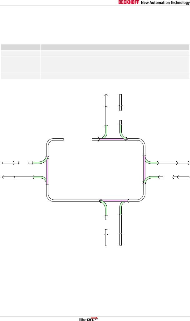
The ET1100 ASIC is an EtherCAT Slave Controller (ESC). It takes care of the EtherCAT communication as an interface between the EtherCAT fieldbus and the slave application. The ET1100 supports a wide range of applications. For example, it may be used as a 32 bit Digital I/O node without external logic using Distributed clocks, or as a part of a complex µController design with up to 4 EtherCAT communication ports.
Feature
Ports
FMMUs
SyncManagers
RAM
Distributed Clocks
Process Data Interfaces
Power supply
I/O
Package
Other features
Table 1: ET1100 Main Features
ET1100
2-4 ports (each EBUS or MII)
8
8
8 Kbyte
Yes, 64 bit (power saving options with SII EEPROM configuration)
32 Bit Digital I/O (unidirectional/bidirectional)
SPI Slave
8/16 asynchronous/synchronous µController
Integrated voltage regulator (LDO) for logic core/PLL (5V/3.3V to 2.5V), optional external power supply for logic core/PLL.
3.3V compatible I/O
BGA128 (10x10 mm2)
Internal 1GHz PLL
Clock output for external devices (10, 20, 25 MHz)
The general functionality of the ET1100 EtherCAT Slave Controller (ESC) is shown in Figure 1:
EBUS/MII ports
|
|
0 |
1 |
2 |
3 |
SPI / µC / Digital I/O |
|
|
AutoForwarder + |
PDI |
|||
|
|
|
Loopback |
|
||
|
PHY MI |
|
|
|
||
|
|
|
|
|
|
|
|
|
|
|
ECAT Interface |
PDI Interface |
|
|
PHY |
|
|
|
|
|
|
Management |
|
|
|
|
|
|
|
|
|
FMMU |
|
|
|
ECAT |
|
|
|
SyncManager |
|
|
|
|
|
|
|
|
|
Processing |
|
|
|
|
|
|
Unit |
|
|
|
|
|
|
|
|
|
ESC address space |
||
Reset |
Reset |
|
Registers |
User RAM |
Process RAM |
|
|
Monitoring |
Distributed |
|
EEPROM |
Status |
|
|
Clocks |
|
||||
|
|
|
|
|
||
|
|
SYNC |
LATCH |
I²C EEPROM |
LEDs |
|
Figure 1: ET1100 Block Diagram
Slave Controller – ET1100 Hardware Description |
III-1 |
Overview
1.1Frame processing order
The frame processing order of the ET1100 depends on the number of ports and the chip mode (logical port numbers are used):
Table 2: Frame Processing Order
Number of Ports Frame processing order
20→EtherCAT Processing Unit→1 / 1→0
30→EtherCAT Processing Unit→1 / 1→2 / 2→0 (log. ports 0,1, and 2) or
0→EtherCAT Processing Unit→3 / 3→1 / 1→0 (log. ports 0,1, and 3)
40→EtherCAT Processing Unit→3 / 3→1 / 1→2 / 2→0
Figure 2 shows the frame processing in general:
Port 0
Forwarder
Auto-
port 0 open or all ports closed |
port 0 closed |
Loopback function |
|
Port 3 |
|
1 |
|
Auto- |
|
Forwarder |
|
port 3 open |
EtherCAT |
|
Processing Unit |
port 3 closed |
|
Loopback function |
EtherCAT
Slave Controller
Loopback function
port 2 closed
Loopback function |
port 1 closed |
open |
-Auto Forwarder |
port1 |
|
|
1 |
Port 1
port 2 open
Auto-
Forwarder
Port 2
Figure 2: Frame Processing
III-2 |
Slave Controller – ET1100 Hardware Description |

Overview
1.2Scope of this document
This documentation refers to stepping ET1100-0003.
1.3Revision/Build History
|
|
|
|
|
|
Table 3: Revision/Build History |
|||||
|
|
|
|
|
|
|
|
|
|
|
|
|
Revision |
|
|
|
Build |
|
|
|
|
Stepping |
|
|
Register 0x0001 |
|
|
|
Register 0x0002:0x0003 |
|
|
|
|
||
|
|
|
|
|
|
|
|
|
|||
|
|
|
|
|
|
|
|
|
|||
|
0x00 |
|
|
|
0x0000 |
|
|
|
|
ET1100-0000 or |
|
|
|
|
|
|
|
|
|
|
|
ET1100-0001 |
|
|
|
|
|
|
|
|
|
|
|||
|
0x00 |
|
|
|
0x0002 |
|
|
|
|
ET1100-0002 |
|
|
|
|
|
|
|
|
|
|
|||
|
0x00 |
|
|
|
0x0003 |
|
|
|
|
ET1100-0003 |
|
|
|
|
|
|
|
|
|
|
|
|
|
The stepping code is printed on the devices, do not confuse the stepping code with the ordering codes.
Slave Controller – ET1100 Hardware Description |
III-3 |

Features and Registers
2 Features and Registers
2.1Features
Table 4: ET1100 Feature Details
Feature
EtherCAT Ports
Permanent ports
Optional Bridge port 3 (EBUS or MII)
EBUS ports
MII ports
RMII ports
RGMII ports
Port 0
Ports 0, 1
Ports 0, 1, 2
Ports 0, 1, 3
Ports 0, 1, 2, 3
Slave Category
Position addressing
Node addressing
Logical addressing
Broadcast addressing
Physical Layer General Features
FIFO Size configurable (0x0100[18:16])
FIFO Size default from SII EEPROM
Auto-Forwarder checks CRC and SOF
Forwarded RX Error indication, detection and Counter (0x0308:0x030B)
Lost Link Counter (0x0310:0x0313)
Prevention of circulating frames
Fallback: Port 0 opens if all ports are closed
VLAN Tag and IP/UDP support
Enhanced Link Detection per port configurable
EBUS Features
Low Jitter
Enhanced Link Detection supported
Enhanced Link Detection compatible
EBUS signal validation
LVDS Transceiver internal
LVDS sample rate [MHz]
Remote link down signaling time configurable 0x0100[22]
General Ethernet Features (MII/RMII/RGMII)
MII Management Interface (0x0510:0x051F)
Supported PHY Address Offsets
Individual port PHY addresses
Port PHY addresses readable
Link Polarity configurable
Enhanced Link Detection supported
FX PHY support (native)
PHY reset out signals
Link detection using PHY signal (LED)
MI link status and configuration
MI controllable by PDI (0x0516:0x0517)
MI read error (0x0510.13)
MI PHY configuration update status (0x0518.5)
MI preamble suppression
Additional MCLK
Gigabit PHY configuration
Gigabit PHY register 9 relaxed check
FX PHY configuration
Transparent Mode
ET1100 -0003
2-4
2-4
-
0-4
0-4
-
-
-
x
x x
x
Full Slave
x
x
x x
x
-
x
x
x
x
x
x
-
x
-
x
x x
1,000
x
x
0/16
-
-
x x
-
-
x
-
-
-
-
-
x
-
-
-
x
|
Feature |
|
|
|
ET1100 |
|
|
|
|
|
-0003 |
|
|
|
|
|
|
|
|
|
|
|
|
|
|
|
|
|
MII Features |
|
|
|
|
|
|
|
|
|
|
||
|
CLK25OUT as PHY clock source |
|
|
|
x |
|
|
|
|
|
|
||
|
Bootstrap TX Shift settings |
|
|
|
x |
|
|
|
|
|
|||
|
Automatic TX Shift setting (with TX_CLK) |
|
|
|
- |
|
|
|
|
|
|
|
|
|
TX Shift not necessary (PHY TX_CLK as |
|
|
|
- |
|
|
clock source) |
|
|
|
|
|
|
|
|
|
|
|
|
|
|
|
|
|||
|
FIFO size reduction steps |
|
|
|
1 |
|
|
|
|
|
|
|
|
|
PDI General Features |
|
|
|
|
|
|
|
|
|
|
|
|
Increased PDI performance
Extended PDI Configuration (0x0152:0x0153)
PDI Error Counter (0x030D)
PDI Error Code (0x030E)
CPU_CLK output (10, 20, 25 MHz)
SOF, EOF, WD_TRIG and WD_STATE independent of PDI
Available PDIs and PDI features depending on port configuration
PDI selection at run-time (SII EEPROM)
PDI active immediately (SII EEPROM settings ignored)
PDI function acknowledge by write
PDI Information register 0x014E:0x014F
Digital I/O PDI
Digital I/O width [bits]
PDI Control register value (0x0140:0x0141)
Control/Status signals:
LATCH_IN
SOF
OUTVALID
WD_TRIG
OE_CONF
OE_EXT
EEPROM_
Loaded
WD_STATE
EOF
Granularity of direction configuration [bits] Bidirectional mode
Output high-Z if WD expired
Output 0 if WD expired
Output with EOF
Output with DC SyncSignals
Input with SOF
Input with DC SyncSignals
-
x
x
-
x
-
x
x
-
-
-
x
8/16/24/32
4
7/01
x1
x1
x1
x1
x1
x1
x1
-
-
2 x x
x x x
x x
1 Availability depending on port configuration
III-4 |
Slave Controller – ET1100 Hardware Description |

Features and Registers
Feature
SPI Slave PDI
Max. SPI clock [MHz]
SPI modes configurable (0x0150[1:0])
SPI_IRQ driver configurable (0x0150[3:2])
SPI_SEL polarity configurable (0x0150.4)
Data out sample mode configurable (0x0150.5)
Busy signaling
Wait State byte(s)
Number of address extension byte(s)
2/4 Byte SPI master support
Extended error detection (read busy violation)
SPI_IRQ delay
Status indication
EEPROM_
Loaded signal
Asynchronous µController PDI
Extended µC configuration bits 0x0150[7:4], 0x0152:0x0153
ADR[15:13] available (000b if not
available)
EEPROM_Loaded signal
RD polarity configurable (0x0150.7)
Read BUSY delay (0x0152.0)
Write after first edge (0x0152.2)
Synchronous µController PDI
EEPROM_
Loaded signal
EtherCAT Bridge (port 3, EBUS/MII)
General Purpose I/O
GPO bits
GPI bits
GPIO available independent of PDI or port configuration
GPIO available without PDI
Concurrent access to GPO by ECAT and PDI
ESC Information
Basic Information (0x0000:0x0006)
Port Descriptor (0x0007)
ESC Features supported (0x0008:0x0009)
Extended ESC Feature Availability in User RAM (0x0F80 ff.)
Write Protection (0x0020:0x0031)
Data Link Layer Features
ECAT Reset (0x0040)
PDI Reset (0x0041)
ESC DL Control (0x0100:0x0103) bytes
EtherCAT only mode (0x0100.0)
Temporary loop control (0x0100.1)
FIFO Size configurable (0x0100[18:16])
Configured Station Address (0x0010:0x0011)
Configured Station Alias (0x0100.24, 0x0012:0x0013)
Physical Read/Write Offset (0x0108:0x0109)
Application Layer Features
Extended AL Control/Status bits (0x0120[15:5], 0x0130[15:5])
AL Status Emulation (0x0140.8)
AL Status Code (0x0134:0x0135)
ET1100 -0003
x
20
x x
x
x
-
x any
x
x
x x
x
8/16 bit
x
x
x
x x
-
8/16 bit
x
-
x
0-16
0-16
-
-
x
x x
x
-
x
x
-
4
x
x
x
x
x
x
x
x
x
Feature
Interrupts
ECAT Event Mask (0x0200:0x0201)
AL Event Mask (0x0204:0x0207)
ECAT Event Request (0x0210:0x0211)
AL Event Request (0x0220:0x0223)
SyncManager activation changed (0x0220.4)
SyncManager watchdog expiration (0x0220.6)
Error Counters
RX Error Counter (0x0300:0x0307)
Forwarded RX Error Counter (0x0308:0x030B)
ECAT Processing Unit Error Counter (0x030C)
PDI Error Counter (0x030D)
Lost Link Counter (0x0310:0x0313)
Watchdog
Watchdog Divider configurable (0x0400:0x0401)
Watchdog Process Data
Watchdog PDI
Watchdog Counter Process Data (0x0442)
Watchdog Counter PDI (0x0443)
SII EEPROM Interface (0x0500:0x050F)
EEPROM sizes supported
EEPROM size reflected in 0x0502.7
EEPROM controllable by PDI
EEPROM Emulation by PDI
Read data bytes (0x0502.6)
Internal Pull-Ups for EEPROM_CLK and EEPROM_DATA
FMMUs
Bit-oriented operation
SyncManagers
Watchdog trigger generation for 1 Byte Mailbox configuration independent of reading access
SyncManager Event Times (+0x8[7:6])
Buffer state (+0x5[7:6])
Distributed Clocks
Width
Sync/Latch signals
SyncManager Event Times (0x09F0:0x09FF)
DC Receive Times
DC Time Loop Control controllable by PDI
DC activation by EEPROM (0x0140[11:10])
Propagation delay measurement with traffic (BWR/FPWR 0x900 detected at each port)
LatchSignal state in Latch Status register (0x09AE:0x09AF)
SyncSignal Auto-Activation (0x0981.3)
SyncSignal 32 or 64 bit Start Time (0x0981.4)
SyncSignal Late Activation (0x0981[6:5])
SyncSignal debug pulse (0x0981.7)
SyncSignal Activation State 0x0984)
Reset filters after writing filter depth
ESC Specific Registers (0x0E00:0x0EFF)
Product and Vendor ID
POR Values
FPGA Update (online)
Process RAM and User RAM
Process RAM (0x1000 ff.) [Kbyte]
User RAM (0x0F80:0x0FFF)
Extended ESC Feature Availability in User
RAM
ET1100 -0003
x
x x
x
x
-
x
x
x
x x
x
x x x
x
1 Kbyte-
4 Mbyte
x
x
-
8
x
8
x
8
x
x
-
x
64
2
x
x
-
x
x
x
-
-
-
-
-
-
-
x
-
8
x
-
|
|
|
|
|
|
|
|
|
|
|
|
|
|
|
|
|
|
|
|
|
|
|
|
|
|
|
|
Slave Controller – ET1100 Hardware Description |
|
III-5 |
|||||

Features and Registers
Feature
Additional EEPROMs
SII EEPROM (I²C)
FPGA configuration EEPROM
LED Signals
RUN LED
RUN LED override
Link/Activity(x) LED per port
PERR(x) LED per port
Device ERR LED
STATE_RUN LED
Optional LED states
RUN LED: Bootstrap
RUN LED: Booting
RUN LED: Device identification
RUN LED: loading SII EEPROM
Error LED: SII EEPROM loading error
Error LED: Invalid hardware configuration
Error LED: Process data watchdog timeout
Error LED: PDI watchdog timeout
Link/Activity: port closed
Link/Activity: local auto-negotiation error
Link/Activity: remote auto-negotiation error
Link/Activity: unknown PHY autonegotiation error
LED test
ET1100 -0003
1
x
-
x
-
x
x
-
-
x
-
-
-
-
-
-
-
-
-
-
-
-
|
Feature |
|
|
|
ET1100 |
|
|
|
|
|
-0003 |
|
|
|
|
|
|
|
|
|
|
|
|
|
|
|
|
|
Clock supply |
|
|
|
|
|
|
|
|
|
|
||
|
Crystal |
|
|
|
x |
|
|
|
|
|
|
||
|
Crystal oscillator |
|
|
|
x |
|
|
|
|
|
|
||
|
TX_CLK from PHY |
|
|
|
x |
|
|
|
|
|
|
||
|
25ppm clock source accuracy |
|
|
|
x |
|
|
|
|
|
|
||
|
Internal PLL |
|
|
|
x |
|
|
|
|
|
|||
|
Power Supply Voltages |
|
|
|
1-2 |
|
|
|
|
|
|
|
|
|
I/O Voltage |
|
|
|
|
|
|
|
|
|
|
||
|
3.3 V |
|
|
|
x |
|
|
|
|
|
|||
|
3.3V / 5V tolerant |
|
|
|
- |
|
|
|
|
|
|
||
|
5 V |
|
|
|
(x) |
|
|
|
|
|
|
||
|
Core Voltage |
|
|
|
2.5V |
|
|
|
|
|
|||
|
Internal LDOs |
|
|
|
1 |
|
|
|
|
|
|
||
|
LDO supply voltage |
|
|
|
3.3V/5V |
|
|
|
|
|
|
||
|
Core Voltage |
|
|
|
x |
|
|
|
|
|
|||
|
I/O Voltage |
|
|
|
- |
|
|
|
|
|
|
||
|
Package |
|
|
|
BGA128 |
|
|
|
|
|
|
||
|
Size [mm²] |
|
|
|
10x10 |
|
|
|
|
|
|||
|
Original Release date |
|
|
|
3/2007 |
|
|
|
|
|
|
||
|
Configuration and Pinout calculator (XLS) |
|
|
|
x |
|
|
|
|
|
|
||
|
Register Configuration |
|
|
|
fixed |
|
|
|
|
|
|
|
|
Table 5: Legend
Symbol Description
x available
-not available
c configurable
III-6 |
Slave Controller – ET1100 Hardware Description |
Features and Registers
2.2Registers
An EtherCAT Slave Controller (ESC) has an address space of 64 Kbyte. The first block of 4 Kbyte (0x0000:0x0FFF) is dedicated for registers. The process data RAM starts at address 0x1000, its size is 8 Kbyte (end address 0x2FFF).
Table 7 gives an overview of the available registers.
Table 6: Register Overview Legend
Symbol Description
x Available
-Not available
sAvailable if DC SYNC Out Unit enabled (Register 0x0140.10=1)
lAvailable if DC Latch In Unit enabled (Register 0x0140.11=1)
|
s/l |
|
|
|
Available if DC SYNC Out Unit enabled and/or |
|
|
|
|
|
|
||
|
|
|
|
|
DC Latch In Unit enabled |
|
|
|
|
|
|
(Register 0x0140.10=1 and/or 0x0140.11=1) |
|
|
|
|
|
|
|
|
|
Table 7: Register Overview |
|
|
Address |
Length |
Description |
|
|
(Byte) |
|
ET1100 |
|
|
|
|
0x0000 |
1 |
Type |
x |
0x0001 |
1 |
Revision |
x |
0x0002:0x0003 |
2 |
Build |
x |
0x0004 |
1 |
FMMUs supported |
x |
0x0005 |
1 |
SyncManagers supported |
x |
0x0006 |
1 |
RAM Size |
x |
0x0007 |
1 |
Port Descriptor |
x |
0x0008:0x0009 |
2 |
ESC Features supported |
x |
0x0010:0x0011 |
2 |
Configured Station Address |
x |
0x0012:0x0013 |
2 |
Configured Station Alias |
x |
0x0020 |
1 |
Write Register Enable |
x |
0x0021 |
1 |
Write Register Protection |
x |
0x0030 |
1 |
ESC Write Enable |
x |
0x0031 |
1 |
ESC Write Protection |
x |
0x0040 |
1 |
ESC Reset ECAT |
x |
0x0041 |
1 |
ESC Reset PDI |
- |
0x0100:0x0101 |
2 |
ESC DL Control |
x |
0x0102:0x0103 |
2 |
Extended ESC DL Control |
x |
0x0108:0x0109 |
2 |
Physical Read/Write Offset |
x |
0x0110:0x0111 |
2 |
ESC DL Status |
x |
0x0120 |
5 bits |
AL Control |
x |
|
[4:0] |
|
|
0x0120:0x0121 |
2 |
AL Control |
x |
0x0130 |
5 bits |
AL Status |
x |
|
[4:0] |
|
|
Slave Controller – ET1100 Hardware Description |
III-7 |

Features and Registers
Address |
Length |
|
(Byte) |
0x0130:0x0131 |
2 |
0x0134:0x0135 |
2 |
0x0138 |
1 |
0x0139 |
1 |
0x0140 |
1 |
0x0141 |
1 |
0x014E:0x014F |
2 |
0x0150 |
1 |
0x0151 |
1 |
0x0152:0x0153 |
2 |
0x0200:0x0201 |
2 |
0x0204:0x0207 |
4 |
0x0210:0x0211 |
2 |
0x0220:0x0223 |
4 |
0x0300:0x0307 |
4x2 |
0x0308:0x030B |
4x1 |
0x030C |
1 |
0x030D |
|
1 |
|
|
|
0x030E |
|
1 |
|
|
|
0x0310:0x0313 |
|
4x1 |
|
|
|
0x0400:0x0401 |
|
2 |
|
|
|
0x0410:0x0411 |
|
2 |
|
|
|
0x0420:0x0421 |
|
2 |
|
|
|
0x0440:0x0441 |
|
2 |
|
|
|
0x0442 |
|
1 |
|
|
|
|
|
|
0x0443 |
1 |
0x0500:0x050F |
16 |
0x0510:0x0515 |
6 |
0x0516:0x0517 |
2 |
0x0518:0x051B |
4 |
0x0600:0x06FC |
16x13 |
0x0800:0x087F |
16x8 |
0x0900:0x090F |
4x4 |
0x0918:0x091F |
8 |
0x0920:0x0935 |
24 |
0x0910:0x0917 |
8 |
0x0936 |
1 |
0x0980 |
1 |
0x0981 |
1 |
Description |
|
|
ET1100 |
AL Status |
x |
AL Status Code |
x |
RUN LED Override |
- |
ERR LED Override |
- |
PDI Control |
x |
ESC Configuration |
x |
PDI Information |
- |
PDI Configuration |
x |
DC Sync/Latch Configuration |
x |
Extended PDI Configuration |
x |
ECAT Event Mask |
x |
PDI AL Event Mask |
x |
ECAT Event Request |
x |
AL Event Request |
x |
Rx Error Counter[3:0] |
x |
Forwarded Rx Error |
x |
counter[3:0] |
|
ECAT Processing Unit Error |
x |
Counter |
|
PDI Error Counter |
x |
PDI Error Code |
- |
Lost Link Counter[3:0] |
x |
Watchdog Divider |
x |
Watchdog Time PDI |
x |
Watchdog Time Process Data |
x |
Watchdog Status Process Data |
x |
Watchdog Counter Process |
x |
Data |
|
Watchdog Counter PDI |
x |
SII EEPROM Interface |
x |
MII Management Interface |
x |
MII Management Access State |
- |
PHY Port Status[3:0] |
- |
FMMU[15:0] |
8 |
SyncManager[15:0] |
8 |
DC – Receive Times[3:0] |
x |
DC – Receive Time EPU |
s/l |
DC – Time Loop Control Unit |
s/l |
DC – System Time |
s/l |
DC – Receive Time Latch |
- |
mode |
|
DC – Cyclic Unit Control |
s |
DC – Activation |
s |
III-8 |
Slave Controller – ET1100 Hardware Description |

Features and Registers
Address |
Length |
|
(Byte) |
0x0982:0x0983 |
2 |
0x0984 |
1 |
0x098E:0x09A7 |
26 |
0x09A8 |
1 |
0x09A9 |
1 |
0x09AE |
1 |
0x09B0:0x09B7 |
8 |
0x09B8:0x09BF |
8 |
0x09C0:0x09C7 |
8 |
0x09C7:0x09CF |
8 |
0x09F0:0x09F3 |
12 |
0x09F8:0x09FF |
|
0x0E00:0x0E03 |
4 |
0x0E00:0x0E07 |
8 |
0x0E08:0x0E0F |
8 |
0x0E10 |
1 |
0x0F00:0x0F03 |
4 |
0x0F10:0x0F17 |
8 |
0x0F18:0x0F1F 8 0x0F80:0x0FFF 128 0x1000:0x1003 4
0x1000 ff.
Description
ET1100
DC – Pulse length of |
s |
SyncSignals |
|
DC – Activation Status |
- |
DC – SYNC Out Unit |
s |
DC – Latch0 Control |
l |
DC – Latch1 Control |
l |
DC – Latch0 Status |
l |
DC – Latch0 Positive Edge |
l |
DC – Latch0 Negative Edge |
l |
DC – Latch1 Positive Edge |
l |
DC – Latch1 Negative Edge |
l |
DC – SyncManager Event |
s/l |
Times |
|
Power-On Values (Bits) |
16 |
Product ID |
- |
Vendor ID |
- |
ESC Health Status |
- |
Digital I/O Output Data |
x |
General Purpose Outputs |
2 |
[Byte] |
|
General Purpose Inputs [Byte] |
2 |
User RAM |
x |
Digital I/O Input Data |
io |
Process Data RAM [Kbyte] |
8 |
Slave Controller – ET1100 Hardware Description |
III-9 |

Pin Description
3 Pin Description
For pin configuration there is a table calculation file (ET1100 configuration and pinout V<version>.xls) available to make pin configuration easier. This file can be downloaded from the Beckhoff homepage (http://www.beckhoff.com). This documentation supersedes the table calculation file.
Input pins should not be left open/floating. Unused input pins (denoted with direction UI) without external or internal pull-up/pull-down resistor should not be left open. Unused configuration pins should be pulled down if the application allows this (take care of configuration signals in the PDI[39:0] area when bidirectional Digital I/O is used). Unused PDI[39:0] input pins should be pulled down, all other input pins can be connected to GND directly.
Pull-up resistors must connect to VCC I/O, not to a different power source. Otherwise the ET1100 could be powered via the resistors and the internal clamping diodes as long as VCC I/O is below the other power source.
Internal pull-up/pull-down resistor values shown in the pinout tables are nominal.
3.1Overview
3.1.1Pin Overview
|
|
Table 8: Pin Overview |
|
|
||
Pin |
Pin name |
Dir. |
Pin |
Pin name |
Dir. |
|
A1 |
PDI[27]/RX_DV(3)/EBUS(3)-RX- |
BD/LI- |
D7 |
GNDCore |
|
|
A2 |
PDI[26]/TX_ENA(3)/EBUS(3)-TX+ |
BD/LO+ |
D8 |
Res. [7] |
I |
|
A3 |
PDI[24]/TX_D(3)[1]/EBUS(3)-TX- |
BD/LO- |
D9 |
GNDI/O |
|
|
A4 |
PDI[22]/TX_D(3)[3] |
BD |
D10 |
VCC I/O |
|
|
A5 |
PDI[20]/RX_D(3)[3] |
BD |
D11 |
PDI[1] |
BD |
|
A6 |
PDI[18]/RX_D(3)[0] |
BD |
D12 |
PDI[0] |
BD |
|
A7 |
PDI[16]/RX_ERR(3) |
BD |
E1 |
TX_D(2)[1]/EBUS(2)-TX- |
O/LO- |
|
A8 |
PDI[14] |
BD |
E2 |
PDI[34]/TX_D(2)[0]/ |
BD |
|
CTRL_STATUS_MOVE |
||||||
|
|
|
|
|
||
A9 |
PDI[12] |
BD |
E3 |
LINKACT(2)/P_CONF[2] |
BD |
|
A10 |
PDI[10] |
BD |
E4 |
Res. [0] |
I |
|
A11 |
PDI[8] |
BD |
E9 |
VCC I/O |
|
|
A12 |
PDI[6] |
BD |
E10 |
Res. [3] |
I |
|
B1 |
PDI[29]/RX_D(3)[1]/EBUS(3)-RX+ |
BD/LI+ |
E11 |
SYNC/LATCH[0] |
BD |
|
B2 |
PDI[28]/PERR(3)/TRANS(3) |
BD |
E12 |
SYNC/LATCH[1] |
BD |
|
B3 |
PDI[25]/TX_D(3)[0] |
BD |
F1 |
TX_ENA(2)/EBUS(2)-TX+ |
BD/LO+ |
|
B4 |
PDI[23]/TX_D(3)[2] |
BD |
F2 |
LINK_MII(2)/CLK25OUT1 |
BD |
|
B5 |
PDI[21]/LINK_MII(3) |
BD |
F3 |
VCC I/O (T0) |
|
|
B6 |
PDI[19]/RX_D(3)[2] |
BD |
F4 |
Res. [6] |
I |
|
B7 |
PDI[17]/RX_CLK(3) |
BD |
F9 |
GNDI/O |
|
|
B8 |
PDI[15] |
BD |
F10 |
VCC I/O |
|
|
B9 |
PDI[13] |
BD |
F11 |
EEPROM_DATA |
BD |
|
B10 |
PDI[9] |
BD |
F12 |
OSC_OUT |
O |
|
B11 |
PDI[7]/CPU_CLK |
BD |
G1 |
PDI[35]/RX_ERR(2) |
BD |
|
B12 |
PDI[4] |
BD |
G2 |
PDI[36]/RX_CLK(2) |
BD |
|
C1 |
PDI[31]/CLK25OUT2 |
BD |
G3 |
Res. [1] |
I |
|
C2 |
PDI[30]/LINKACT(3)/P_CONF(3) |
BD |
G4 |
Res. [2] |
I |
|
C3 |
PERR(2)/TRANS(2)/PHYAD_OFF |
BD |
G9 |
GNDPLL |
|
|
C4 |
RBIAS |
|
G10 |
VCC PLL |
|
|
C5 |
VCC I/O |
|
G11 |
EEPROM_CLK |
BD |
|
C6 |
VCC Core |
|
G12 |
OSC_IN |
I |
|
C7 |
VCC Core |
|
H1 |
RX_DV(2)/EBUS(2)-RX- |
I/LI- |
|
C8 |
Res. [4] |
I |
H2 |
PDI[37]/RX_D(2)[0] |
BD |
|
C9 |
PDI[11] |
BD |
H3 |
TESTMODE |
I |
|
C10 |
PDI[5] |
BD |
H4 |
GNDI/O (T1) |
|
|
III-10 |
|
|
Slave Controller – ET1100 Hardware Description |
|||

Pin Description
Pin |
Pin name |
Dir. |
C11 |
PDI[3] |
BD |
C12 |
PDI[2] |
BD |
D1 |
PDI[32]/TX_D(2)[3] |
BD |
D2 |
PDI[33]/TX_D(2)[2] |
BD |
D3 |
VCC I/O |
|
D4 |
GNDI/O |
|
D5 |
GNDI/O |
|
D6 |
GNDCore |
|
J5 |
GNDI/O |
|
J6 |
GNDCore |
|
J7 |
GNDCore |
|
J8 |
GNDI/O |
|
J9 |
GNDI/O |
|
J10 |
VCC I/O |
|
J11 |
PERR (0)/TRANS(0)/CLK_MODE[0] |
BD |
J12 |
LINKACT(0)/P_CONF[0] |
BD |
K1 |
PDI[39]/RX_D(2)[3] |
BD |
K2 |
PERR(1)/TRANS(1)/CLK_MODE(1) |
BD |
K3 |
LINK_MII(1) |
I |
K4 |
RX_CLK(1) |
I |
K5 |
VCC I/O |
|
K6 |
VCC Core |
|
K7 |
VCC Core |
|
K8 |
VCC I/O |
|
K9 |
GNDI/O (T2) |
|
K10 |
RX_D(0)[0] |
I |
K11 |
MI_CLK/LINKPOL |
BD |
K12 |
MI_DATA |
BD |
L1 |
LINKACT(1)/P_CONF(1) |
BD |
L2 |
TX_D(1)[2]/P_MODE[0] |
BD |
Pin |
Pin name |
Dir. |
H9 |
VCC I/O (T3) |
|
H10 |
Res. [5] |
I |
H11 |
RUN/EEPROM_SIZE |
BD |
H12 |
RESET |
BD |
J1 |
RX_D(2)[1]/EBUS(2)-RX+ |
I/LI+ |
J2 |
PDI[38]/RX_D(2)[2] |
BD |
J3 |
VCC I/O |
|
J4 |
GNDI/O |
|
L3 |
TX_D(1)[0]/TRANS_MODE_ENA BD |
|
L4 |
RX_D(1)[0] |
I |
L5 |
RX_D(1)[2] |
I |
L6 |
RX_ERR(1) |
I |
L7 |
TX_D(0)[2]/C25_SHI[0] |
BD |
L8 |
TX_D(0)[0]/C25_ENA |
BD |
L9 |
LINK_MII(0) |
I |
L10 |
RX_CLK(0) |
I |
L11 |
RX_D(0)[2] |
I |
L12 |
RX_D(0)[3] |
I |
M1 |
TX_D(1)[3]/P_MODE[1] |
BD |
M2 |
TX_D(1)[1]/EBUS(1)-TX- |
O/LO- |
M3 |
TX_ENA(1)/EBUS(1)-TX+ |
BD/LO+ |
M4 |
RX_DV(1)/EBUS(1)-RX- |
I/LI- |
M5 |
RX_D(1)[1]/EBUS(1)-RX+ |
I/LI+ |
M6 |
RX_D(1)[3] |
I |
M7 |
TX_D(0)[3]/C25_SHI[1] |
BD |
M8 |
TX_D(0)[1]/EBUS(0)-TX- |
O/LO- |
M9 |
TX_ENA(0)/EBUS(0)-TX+ |
BD/LO+ |
M10 |
RX_ERR(0) |
I |
M11 |
RX_DV(0)/EBUS(0)-RX- |
I/LI- |
M12 |
RX_D(0)[1]/EBUS(0)-RX+ |
I/LI+ |
Slave Controller – ET1100 Hardware Description |
III-11 |

Pin Description
3.1.2Signal Overview
Table 9: Signal Overview
|
Signal |
|
|
|
Type |
|
|
|
Dir. |
|
|
|
Description |
|
|
|
|
|
|
|
|
|
|
|
|
||||
|
|
|
|
|
|
|
|
|
|
|||||
|
C25_ENA |
|
|
|
Configuration |
|
|
|
I |
|
|
|
CLK25OUT2 Enable: Enable CLK25OUT2 |
|
|
|
|
|
|
|
|
|
|
|
|||||
|
C25_SHI[1:0] |
|
|
|
Configuration |
|
|
|
I |
|
|
|
TX Shift: Shifting/phase compensation of MII TX signals |
|
|
|
|
|
|
|
|
|
|
|
|||||
|
CLK_MODE[1:0] |
|
|
|
Configuration |
|
|
|
I |
|
|
|
CPU_CLK configuration |
|
|
|
|
|
|
|
|
|
|
|
|||||
|
CLK25OUT1/CLK25OUT2 |
|
|
|
MII |
|
|
|
O |
|
|
|
25 MHz clock source for Ethernet PHYs |
|
|
|
|
|
|
|
|
|
|
|
|||||
|
CPU_CLK |
|
|
|
PDI |
|
|
|
O |
|
|
|
Clock signal for µController |
|
|
|
|
|
|
|
|
|
|
|
|||||
|
CTRL_STATUS_MOVE |
|
|
|
Configuration |
|
|
|
I |
|
|
|
Move Digital I/O Control/Status signal to last available PDI byte |
|
|
|
|
|
|
|
|
|
|
|
|||||
|
EBUS(3:0)-RX- |
|
|
|
EBUS |
|
|
|
LI- |
|
|
|
EBUS LVDS receive signal - |
|
|
|
|
|
|
|
|
|
|
|
|||||
|
EBUS(3:0)-RX+ |
|
|
|
EBUS |
|
|
|
LI+ |
|
|
|
EBUS LVDS receive signal + |
|
|
|
|
|
|
|
|
|
|
|
|||||
|
EBUS(3:0)-TX- |
|
|
|
EBUS |
|
|
|
LO- |
|
|
|
EBUS LVDS transmit signal - |
|
|
|
|
|
|
|
|
|
|
|
|||||
|
EBUS(3:0)-TX+ |
|
|
|
EBUS |
|
|
|
LO+ |
|
|
|
EBUS LVDS transmit signal + |
|
|
|
|
|
|
|
|
|
|
|
|||||
|
EEPROM_CLK |
|
|
|
EEPROM |
|
|
|
BD |
|
|
|
EEPROM I2C Clock |
|
|
|
|
|
|
|
|
|
|
|
|||||
|
EEPROM_DATA |
|
|
|
EEPROM |
|
|
|
BD |
|
|
|
EEPROM I2C Data |
|
|
|
|
|
|
|
|
|
|
|
|||||
|
EEPROM_SIZE |
|
|
|
Configuration |
|
|
|
I |
|
|
|
EEPROM size configuration |
|
|
|
|
|
|
|
|
|
|
|
|||||
|
PERR(3:0) |
|
|
|
LED |
|
|
|
O |
|
|
|
Port receive error LED output (for testing) |
|
|
|
|
|
|
|
|
|
|
|
|
||||
|
GNDCore |
|
|
|
Power |
|
|
|
|
|
|
|
Core logic ground |
|
|
|
|
|
|
|
|
|
|
|
|
||||
|
GNDI/O |
|
|
|
Power |
|
|
|
|
|
|
|
I/O ground |
|
|
|
|
|
|
|
|
|
|
|
|
||||
|
GNDPLL |
|
|
|
Power |
|
|
|
|
|
|
|
PLL ground |
|
|
|
|
|
|
|
|
|
|
|
|||||
|
LINK_MII(3:0) |
|
|
|
MII |
|
|
|
I |
|
|
|
PHY signal indicating a link |
|
|
|
|
|
|
|
|
|
|
|
|||||
|
LINKACT(3:0) |
|
|
|
LED |
|
|
|
O |
|
|
|
Link/Activity LED output |
|
|
|
|
|
|
|
|
|
|
|
|||||
|
LINKPOL |
|
|
|
Configuration |
|
|
|
I |
|
|
|
LINK_MII(3:0) polarity configuration |
|
|
|
|
|
|
|
|
|
|
|
|||||
|
MI_CLK |
|
|
|
MII |
|
|
|
O |
|
|
|
PHY Management Interface clock |
|
|
|
|
|
|
|
|
|
|
|
|||||
|
MI_DATA |
|
|
|
MII |
|
|
|
BD |
|
|
|
PHY Management Interface data |
|
|
|
|
|
|
|
|
|
|
|
|||||
|
OSC_IN |
|
|
|
Clock |
|
|
|
I |
|
|
|
Clock source (crystal/oscillator) |
|
|
|
|
|
|
|
|
|
|
|
|||||
|
OSC_OUT |
|
|
|
Clock |
|
|
|
O |
|
|
|
Clock source (crystal) |
|
|
|
|
|
|
|
|
|
|
|
|||||
|
P_CONF(3:0) |
|
|
|
Configuration |
|
|
|
I |
|
|
|
Physical layer of logical ports |
|
|
|
|
|
|
|
|
|
|
|
|||||
|
P_MODE[1:0] |
|
|
|
Configuration |
|
|
|
I |
|
|
|
Number of physical ports and corresponding logical ports |
|
|
|
|
|
|
|
|
|
|
|
|||||
|
PDI[39:0] |
|
|
|
PDI |
|
|
|
BD |
|
|
|
PDI signal, depending on EEPROM content |
|
|
|
|
|
|
|
|
|
|
|
|||||
|
PHYAD_OFF |
|
|
|
Configuration |
|
|
|
I |
|
|
|
Ethernet PHY Address Offset |
|
|
|
|
|
|
|
|
|
|
|
|
||||
|
RBIAS |
|
|
|
EBUS |
|
|
|
|
|
|
|
BIAS resistor for LVDS TX current adjustment |
|
|
|
|
|
|
|
|
|
|
|
|||||
|
Res. [7:0] |
|
|
|
Reserved |
|
|
|
I |
|
|
|
Reserved pins |
|
|
|
|
|
|
|
|
|
|
|
|||||
|
RESET |
|
|
|
General |
|
|
|
BD |
|
|
|
Open collector Reset output/Reset input |
|
|
|
|
|
|
|
|
|
|
|
|||||
|
RUN |
|
|
|
LED |
|
|
|
O |
|
|
|
Run LED controlled by AL Status register |
|
|
|
|
|
|
|
|
|
|
|
|||||
|
RX_CLK(3:0) |
|
|
|
MII |
|
|
|
I |
|
|
|
MII receive clock |
|
|
|
|
|
|
|
|
|
|
|
|||||
|
RX_D(3:0)[3:0] |
|
|
|
MII |
|
|
|
I |
|
|
|
MII receive data |
|
|
|
|
|
|
|
|
|
|
|
|||||
|
RX_DV(3:0) |
|
|
|
MII |
|
|
|
I |
|
|
|
MII receive data valid |
|
|
|
|
|
|
|
|
|
|
|
|||||
|
RX_ERR(3:0) |
|
|
|
MII |
|
|
|
I |
|
|
|
MII receive error |
|
|
|
|
|
|
|
|
|
|
|
|||||
|
SYNC/LATCH[1:0] |
|
|
|
DC |
|
|
|
I/O |
|
|
|
Distributed Clocks SyncSignal output or LatchSignal input |
|
|
|
|
|
|
|
|
|
|
|
|||||
|
TESTMODE |
|
|
|
General |
|
|
|
I |
|
|
|
Reserved for testing, connect to GND |
|
|
|
|
|
|
|
|
|
|
|
|||||
|
TRANS(3:0) |
|
|
|
MII |
|
|
|
I |
|
|
|
MII interface sharing: share port enable |
|
|
|
|
|
|
|
|
|
|
|
|||||
|
TRANS_MODE_ENA |
|
|
|
Configuration |
|
|
|
I |
|
|
|
Enable MII interface sharing (and TRANS(3:0) signals) |
|
|
|
|
|
|
|
|
|
|
|
|||||
|
TX_D(3:0)[3:0] |
|
|
|
MII |
|
|
|
O |
|
|
|
MII transmit data |
|
|
|
|
|
|
|
|
|
|
|
|||||
|
TX_ENA(3:0) |
|
|
|
MII |
|
|
|
O |
|
|
|
MII transmit enable |
|
|
|
|
|
|
|
|
|
|
|
|
||||
|
VCC Core |
|
|
|
Power |
|
|
|
|
|
|
|
Core logic power |
|
|
|
|
|
|
|
|
|
|
|
|
||||
|
VCC I/O |
|
|
|
Power |
|
|
|
|
|
|
|
I/O power |
|
|
|
|
|
|
|
|
|
|
|
|
||||
|
VCC PLL |
|
|
|
Power |
|
|
|
|
|
|
|
PLL power |
|
III-12 |
Slave Controller – ET1100 Hardware Description |

Pin Description
3.1.3PDI Signal Overview
Table 10: PDI signal overview
PDI |
Signal |
Dir. |
|
|
EEPROM_LOADED |
O |
|
|
I/O[31:0] |
I/O/BD |
|
|
LATCH_IN |
I |
|
Digital I/O |
OE_CONF |
I |
|
OE_EXT |
I |
||
|
|||
|
OUTVALID |
O |
|
|
SOF |
O |
|
|
WD_TRIG |
O |
|
|
EEPROM_LOADED |
O |
|
|
SPI_CLK |
I |
|
SPI |
SPI_DI |
I |
|
SPI_DO |
O |
||
|
|||
|
SPI_IRQ |
O |
|
|
SPI_SEL |
I |
|
|
CS |
I |
|
|
BHE |
I |
|
|
RD |
I |
|
|
WR |
I |
|
µC async. |
BUSY |
O |
|
IRQ |
O |
||
|
|||
|
EEPROM_LOADED |
O |
|
|
DATA[7:0] |
BD |
|
|
ADR[15:0] |
I |
|
|
DATA[15:0] |
BD |
|
|
ADR[15:0] |
I |
|
|
BHE |
I |
|
|
CPU_CLK_IN |
I |
|
|
CS |
I |
|
|
DATA[15:0] |
BD |
|
µC sync. |
DATA[7:0] |
BD |
|
|
EEPROM_LOADED |
O |
|
|
IRQ |
O |
|
|
RD/nWR |
I |
|
|
TA |
O |
|
|
TS |
I |
Description
PDI is active, EEPROM is loaded
Input/Output or Bidirectional data
External data latch signal
Output Enable Configuration
Output Enable
Output data is valid/Output event
Start of Frame
Watchdog Trigger
PDI is active, EEPROM is loaded
SPI clock
SPI data MOSI
SPI data MISO
SPI interrupt
SPI chip select
Chip select
Byte High Enable (16 bit µController interface only)
Read command
Write command
EtherCAT device is busy
Interrupt
PDI is active, EEPROM is loaded
Data bus for 8 bit µController interface
Address bus
Data bus for 16 bit µController interface
Address bus
Byte High Enable
µController interface clock
Chip select
Data bus for 16 Bit µController interface
Data bus for 8 Bit µController interface
PDI is active, EEPROM is loaded
Interrupt
Read/Write access
Transfer Acknowledge
Transfer Start
Slave Controller – ET1100 Hardware Description |
III-13 |

Pin Description
3.2Configuration Pins
The configuration pins are used to configure the ET1100 at power-on with pull-up or pull-down resistors. At power-on the ET1100 uses these pins as inputs to latch the configuration2. After poweron, the pins have their operation functionality which has been assigned to them, and therefore pin direction changes if necessary. The power-on phase finishes before the nRESET pin is released. In subsequent reset phases without power-on condition, the configuration pins still have their operation functionality, i.e., the ET1100 configuration is not latched again and output drivers remain active.
The configuration value 0 is realized by a pull-down resistor, a pull-up resistor is used for a 1. Since some configuration pins are also used as LED outputs, the polarity of the LED output depends on the configuration value.
3.2.1Port Mode
Port Mode configures the number of physical ports and the corresponding logical ports. It is shown in Table 11.
Table 11: Port Mode
|
Description |
|
|
|
Config signal |
|
|
|
Pin name |
|
|
|
Register |
|
|
|
P_MODE[1:0] Values |
|
|
|
|
|
|
|
|
|
|
|
|
|
|
|
|
||||||
|
|
|
|
|
|
|
|
|
|
|
|
|
|
||||||
|
|
|
|
|
P_MODE[0] |
|
|
|
TX_D(1)[2]/P_MODE[0] |
|
|
|
0x0E00[0] |
|
|
|
00 |
= 2 ports (log. ports 0 and 1) |
|
|
Port Mode |
|
|
|
|
|
|
|
|
|
|
|
|
|
|
|
01 |
= 3 ports (log. ports 0,1, and 2) |
|
|
|
|
|
|
|
|
|
|
|
|
|
|
|
|
|
|
|||
|
|
|
|
P_MODE[1] |
|
|
|
TX_D(1)[3]/P_MODE[1] |
|
|
|
0x0E00[1] |
|
|
|
10 |
= 3 ports (log. ports 0,1, and 3) |
|
|
|
|
|
|
|
|
|
|
|
|
|
|
|
|
|
|||||
|
|
|
|
|
|
|
|
|
|
|
|
|
|
|
|
|
11 |
= 4 ports (log. ports 0, 1, 2, and 3) |
|
|
|
|
|
|
|
|
|
|
|
|
|
|
|
|
|
|
|
|
|
NOTE: The term physical port in this document is only used for grouping ET1100 interface pins. The register set as well as any master/slave software is always based on logical ports. The distinction between physical and logical ports is made in order to increase the number of available PDI pins. Each logical port is associated with exactly one physical port, and it can be configured to be either EBUS or MII.
MII ports are always assigned to the lower physical ports, then EBUS ports are assigned. If any MII ports are configured, the lowest logical MII port is always connected to physical port 0, the next higher logical MII port is connected to physical port 1, and so on. Afterwards, the lowest logical EBUS port – if configured – is connected to the next physical port following the physical MII ports, i.e. port [number of MII ports]. Without MII ports, the EBUS ports are connected beginning with physical port 0.
If only EBUS or only MII ports are used, the physical port number is the same as the logical port number for P_MODE[1:0]=00, 01 or 11. Refer to the next chapter for more details.
3.2.2Port Configuration
P_CONF[3:0] determines the physical layer configuration (MII or EBUS). P_CONF[0] determines the physical layer of logical port 0, P_CONF[1] determines logical port 1, P_CONF[2] determines the physical layer of the next available logical port (either 3 for P_MODE[1:0]=10, else 2), and P_CONF[3] determines logical port 3. If a physical port is not used, the corresponding P_CONF configuration signal is not used.
Table 12: Port Configuration
|
Description |
|
|
|
Configuration signal |
|
|
|
Pin name |
|
|
|
Register |
|
|
|
Values |
|
|
|
|
|
|
|
|
|
|
|
|
|
|
|
|
|
|
|
|||
|
|
|
|
|
P_CONF[0] |
|
|
|
LINKACT(0)/P_CONF[0] |
|
|
|
0x0E00[2] |
|
|
|
|
|
|
|
|
|
|
|
|
|
|
|
|
|
|
|
|
|
|
|
|
|
|
|
Port |
|
|
|
P_CONF[1] |
|
|
|
LINKACT(1)/P_CONF(1) |
|
|
|
0x0E00[3] |
|
|
|
0 |
= EBUS |
|
|
Configuration |
|
|
|
|
|
|
|
|
|
|
|
|
1 |
= MII |
|
|||
|
|
|
|
P_CONF[2] |
|
|
|
LINKACT(2)/P_CONF[2] |
|
|
|
0x0E00[4] |
|
|
|
|
|||
|
|
|
|
|
|
|
|
|
|
|
|
|
|
|
|
|
|||
|
|
|
|
|
P_CONF[3] |
|
|
|
PDI[30]/LINKACT(3)/P_CONF(3) |
|
|
|
0x0E00[5] |
|
|
|
|
|
|
|
|
|
|
|
|
|
|
|
|
|
|
|
|
|
|
|
|
|
|
2 Take care of proper configuration: External devices attached to dual-purpose configuration pins might interfere sampling the intended configuration if they are e.g. not properly powered at the sample time (external device keeps configuration pin low although a pull-up resistor is attached). In such cases the ET1100 power-on value sampling time can be delayed by delaying power activation.
III-14 |
Slave Controller – ET1100 Hardware Description |

Pin Description
3.2.2.1Configurations with 2 ports
For configurations with 2 ports, logical ports 0 and 1 are used. The port signals are available at physical ports 0 and 1, depending on the port configuration. P_MODE[1:0] has to be set to 00. P_CONF[1:0] determine the physical layer of logical ports (1:0). P_CONF[3:2] are not used, nevertheless, P_ CONF[2] should not be left open (connection to GND recommended). P_CONF[3] should be pulled down if possible (denoted with ‘-‘ in the table), if your application allows this.
Table 13: Configurations with 2 ports (P_MODE[1:0]=00)
|
Logical port |
|
|
|
|
Physical port |
|
|
|
|
P_CONF |
|
||||||||
|
|
|
|
|
|
|
|
|
|
|
|
|
|
|
|
|
|
|
[3:0] |
|
|
1 |
|
|
|
0 |
|
|
|
|
1 |
|
|
|
0 |
|
|
|
|
|
|
|
|
|
|
|
|
|
|
|
|
|
|
|
|
|
|
|||||
|
|
|
|
|
|
|
|
|
|
|
|
|
|
|||||||
|
EBUS(1) |
|
|
|
EBUS(0) |
|
|
|
|
EBUS(1) |
|
|
|
EBUS(0) |
|
|
|
-000 |
|
|
|
|
|
|
|
|
|
|
|
|
|
|
|
|
|||||||
|
EBUS(1) |
|
|
|
MII(0) |
|
|
|
|
EBUS(1) |
|
|
|
MII(0) |
|
|
|
-001 |
|
|
|
|
|
|
|
|
|
|
|
|
|
|
|
|
|||||||
|
MII(1) |
|
|
|
EBUS(0) |
|
|
|
|
EBUS(0) |
|
|
|
MII(1) |
|
|
|
|
-010 |
|
|
|
|
|
|
|
|
|
|
|
|
|
|
|
|||||||
|
MII(1) |
|
|
|
MII(0) |
|
|
|
|
MII(1) |
|
|
|
MII(0) |
|
|
|
|
-011 |
|
|
|
|
|
|
|
|
|
|
|
|
|
|
|
|
|
|
|
|
|
|
3.2.2.2Configurations with 3 ports
For configurations with 3 ports, either logical ports 0, 1, and 2 (P_MODE[1:0]=01) or logical ports 0, 1, and 3 (P_MODE[1:0]=10) are used. The port signals are available at physical ports 0, 1 and 2, depending on the port configuration. P_CONF[2:0] determine the physical layer of logical ports 2, 1, 0, or logical ports 3, 1, 0, depending on the P_MODE settings (P_CONF[2] is either used for logical port
2 or logical port 3). P_CONF[3] should be pulled down if possible (denoted with ‘-‘ in the tables), if your application allows this.
Table 14: Configurations with 3 ports (ports 0,1, and 2; P_MODE[1:0]=01)
|
|
Logical port |
|
|
|
|
|
Physical port |
|
|
|
|
|
P_CONF |
|
|||||||||||||
|
|
|
|
|
|
|
|
|
|
|
|
|
|
|
|
|
|
|
|
|
|
|
|
|
|
|
[3:0] |
|
|
2 |
|
|
|
1 |
|
|
|
0 |
|
|
|
|
2 |
|
|
|
1 |
|
|
|
0 |
|
|
|
|
|
|
|
|
|
|
|
|
|
|
|
|
|
|
|
|
|
|
|
|
|
|
|
|
|||||||
|
|
|
|
|
|
|
|
|
|
|
|
|
|
|
|
|
|
|||||||||||
|
EBUS(2) |
|
|
|
EBUS(1) |
|
|
|
EBUS(0) |
|
|
|
|
EBUS(2) |
|
|
|
EBUS(1) |
|
|
|
EBUS(0) |
|
|
|
-000 |
|
|
|
|
|
|
|
|
|
|
|
|
|
|
|
|
|
|
|
||||||||||||
|
EBUS(2) |
|
|
|
EBUS(1) |
|
|
|
MII(0) |
|
|
EBUS(2) |
|
|
|
EBUS(1) |
|
|
|
MII(0) |
|
|
-001 |
|
||||
|
|
|
|
|
|
|
|
|
|
|
|
|
|
|
|
|
||||||||||||
|
EBUS(2) |
|
|
|
MII(1) |
|
|
|
EBUS(0) |
|
|
|
|
EBUS(2) |
|
|
|
EBUS(0) |
|
|
|
MII(1) |
|
|
-010 |
|
||
|
|
|
|
|
|
|
|
|
|
|
|
|
|
|
|
|
||||||||||||
|
EBUS(2) |
|
|
|
MII(1) |
|
|
|
MII(0) |
|
|
|
|
EBUS(2) |
|
|
|
MII(1) |
|
|
|
MII(0) |
|
|
-011 |
|
||
|
|
|
|
|
|
|
|
|
|
|
|
|
|
|
|
|
||||||||||||
|
MII(2) |
|
|
|
EBUS(1) |
|
|
|
EBUS(0) |
|
|
|
|
EBUS(1) |
|
|
|
EBUS(0) |
|
|
|
MII(2) |
|
|
-100 |
|
||
|
|
|
|
|
|
|
|
|
|
|
|
|
|
|
|
|
||||||||||||
|
MII(2) |
|
|
|
EBUS(1) |
|
|
|
MII(0) |
|
|
|
|
EBUS(1) |
|
|
|
MII(2) |
|
|
|
MII(0) |
|
|
-101 |
|
||
|
|
|
|
|
|
|
|
|
|
|
|
|
|
|
|
|
||||||||||||
|
MII(2) |
|
|
|
MII(1) |
|
|
|
EBUS(0) |
|
|
|
|
EBUS(0) |
|
|
|
MII(2) |
|
|
|
MII(1) |
|
|
-110 |
|
||
|
|
|
|
|
|
|
|
|
|
|
|
|
|
|
|
|
||||||||||||
|
MII(2) |
|
|
|
MII(1) |
|
|
|
MII(0) |
|
|
|
|
MII(2) |
|
|
|
MII(1) |
|
|
|
MII(0) |
|
|
-111 |
|
||
Table 15: Configurations with 3 ports (ports 0, 1, and 3; P_MODE[1:0]=10)
|
|
|
Logical port |
|
|
|
|
|
Physical port |
|
|
|
|
|
P_CONF |
|
|
|||||||||||||
|
|
|
|
|
|
|
|
|
|
|
|
|
|
|
|
|
|
|
|
|
|
|
|
|
|
|
|
[3:0] |
|
|
|
|
3 |
|
|
|
1 |
|
|
|
0 |
|
|
|
|
2 |
|
|
|
1 |
|
|
|
0 |
|
|
|
|
|
|
|
|
|
|
|
|
|
|
|
|
|
|
|
|
|
|
|
|
|
|
|
|
|
|
||||||||
|
|
|
|
|
|
|
|
|
|
|
|
|
|
|
|
|
|
|
||||||||||||
|
|
EBUS(3) |
|
|
|
EBUS(1) |
|
|
|
EBUS(0) |
|
|
|
|
EBUS(3) |
|
|
|
EBUS(1) |
|
|
|
EBUS(0) |
|
|
|
|
-000 |
|
|
|
|
|
|
|
|
|
|
|
|
|
|
|||||||||||||||||||
|
|
EBUS(3) |
|
|
|
EBUS(1) |
|
|
|
MII(0) |
|
|
|
|
EBUS(3) |
|
|
|
EBUS(1) |
|
|
|
MII(0) |
|
|
|
|
-001 |
|
|
|
|
|
|
|
|
|
|
|
|
|
|
|
|
|
|
|
|
|
||||||||||||
|
|
EBUS(3) |
|
|
|
MII(1) |
|
|
|
EBUS(0) |
|
|
|
|
EBUS(3) |
|
|
|
EBUS(0) |
|
|
|
MII(1) |
|
|
|
|
-010 |
|
|
|
|
|
|
|
|
|
|
|
|
|
|
|
|
|
|
|
|
|
||||||||||||
|
|
EBUS(3) |
|
|
|
MII(1) |
|
|
|
MII(0) |
|
|
|
|
EBUS(3) |
|
|
|
MII(1) |
|
|
|
MII(0) |
|
|
|
|
-011 |
|
|
|
|
|
|
|
|
|
|
|
|
|
|
|
|
|
|
|
|
|
||||||||||||
|
|
MII(3) |
|
|
|
EBUS(1) |
|
|
|
EBUS(0) |
|
|
|
|
EBUS(1) |
|
|
|
EBUS(0) |
|
|
|
MII(3) |
|
|
|
|
-100 |
|
|
|
|
|
|
|
|
|
|
|
|
|
|
|
|
|
|
|
|
|
||||||||||||
|
|
MII(3) |
|
|
|
EBUS(1) |
|
|
|
MII(0) |
|
|
|
|
EBUS(1) |
|
|
|
MII(3) |
|
|
|
MII(0) |
|
|
|
|
-101 |
|
|
|
|
|
|
|
|
|
|
|
|
|
|
|
|
|
|
|
|
|
||||||||||||
|
|
MII(3) |
|
|
|
MII(1) |
|
|
|
EBUS(0) |
|
|
|
|
EBUS(0) |
|
|
|
MII(3) |
|
|
|
MII(1) |
|
|
|
|
-110 |
|
|
|
|
|
|
|
|
|
|
|
|
|
|
|
|
|
|
|
|
|
||||||||||||
|
|
MII(3) |
|
|
|
MII(1) |
|
|
|
MII(0) |
|
|
|
|
MII(3) |
|
|
|
MII(1) |
|
|
|
MII(0) |
|
|
|
|
-111 |
|
|
|
|
|
|
|
|
|
|
|
|
|
|
|
|
|
|
|
|
|
|
|
|
|
|
|
|
|
|
|
|
|
Slave Controller – ET1100 Hardware Description |
|
|
|
|
|
|
|
III-15 |
||||||||||||||||||||||

Pin Description
3.2.2.3Configurations with 4 ports
For configurations with 4 ports, logical ports 0 to 3 are used. The port signals are available at physical ports 0 to 3, depending on the port configuration. P_MODE[1:0] has to be set to 11. P_CONF[3:0] determine the physical layer of logical ports (3:0).
Table 16: Configurations with 4 ports (P_MODE[1:0]=01)
|
|
|
|
|
Logical port |
|
|
|
|
|
|
|
|
|
|
|
Physical port |
|
|
|
|
|
|
|
P_CONF |
|
||||||||||
|
|
|
|
|
|
|
|
|
|
|
|
|
|
|
|
|
|
|
|
|
|
|
|
|
|
|
|
|
|
|
|
|
|
|
[3:0] |
|
|
|
|
|
|
|
|
|
|
|
|
|
|
|
|
|
|
|
|
|
|
|
|
|
|
|
|
|
|
|
|
|
|
|
|||
|
3 |
|
|
|
2 |
|
|
|
1 |
|
|
|
0 |
|
|
|
3 |
|
|
|
2 |
|
|
|
1 |
|
|
|
0 |
|
|
|
|
|
|
|
|
|
|
|
|
|
|
|
|
|
|
|
|
|
|||||||||||||||||||||||
|
EBUS(3) |
|
|
|
EBUS(2) |
|
|
|
EBUS(1) |
|
|
|
EBUS(0) |
|
|
|
|
EBUS(3) |
|
|
|
EBUS(2) |
|
|
|
EBUS(1) |
|
|
|
EBUS(0) |
|
|
|
0000 |
|
|
|
|
|
|
|
|
|
|
|
|
|
|
|
|
|||||||||||||||||||||||
|
EBUS(3) |
|
|
|
EBUS(2) |
|
|
|
EBUS(1) |
|
|
|
MII(0) |
|
|
|
|
EBUS(3) |
|
|
|
EBUS(2) |
|
|
|
EBUS(1) |
|
|
|
MII(0) |
|
|
|
0001 |
|
|
|
|
|
|
|
|
|
|
|
|
|
|
|
|
|
|
|
|
|
|
|||||||||||||||||
|
EBUS(3) |
|
|
|
EBUS(2) |
|
|
|
MII(1) |
|
|
|
EBUS(0) |
|
|
|
|
EBUS(3) |
|
|
|
EBUS(2) |
|
|
|
EBUS(0) |
|
|
|
MII(1) |
|
|
|
0010 |
|
|
|
|
|
|
|
|
|
|
|
|
|
|
|
|
|
|
|
|
|
|
|
|
|
|
|
|
|||||||||||
|
EBUS(3) |
|
|
|
EBUS(2) |
|
|
|
MII(1) |
|
|
|
MII(0) |
|
|
|
|
EBUS(3) |
|
|
|
EBUS(2) |
|
|
|
MII(1) |
|
|
|
MII(0) |
|
|
|
0011 |
|
|
|
|
|
|
|
|
|
|
|
|
|
|
|
|
|
|
|
|
|
|
|||||||||||||||||
|
EBUS(3) |
|
|
|
MII(2) |
|
|
|
EBUS(1) |
|
|
|
EBUS(0) |
|
|
|
|
EBUS(3) |
|
|
|
EBUS(1) |
|
|
|
EBUS(0) |
|
|
|
MII(2) |
|
|
|
0100 |
|
|
|
|
|
|
|
|
|
|
|
|
|
|
|
|
|
|
|
|
|
|
|
|
|
|
|
|
|||||||||||
|
EBUS(3) |
|
|
|
MII(2) |
|
|
|
EBUS(1) |
|
|
|
MII(0) |
|
|
|
|
EBUS(3) |
|
|
|
EBUS(1) |
|
|
|
MII(2) |
|
|
|
MII(0) |
|
|
|
0101 |
|
|
|
|
|
|
|
|
|
|
|
|
|
|
|
|
|
|
|
|
|
|
|
|
|
|
|
|
|||||||||||
|
EBUS(3) |
|
|
|
MII(2) |
|
|
|
MII(1) |
|
|
|
EBUS(0) |
|
|
|
|
EBUS(3) |
|
|
|
EBUS(0) |
|
|
|
MII(2) |
|
|
|
MII(1) |
|
|
|
0110 |
|
|
|
|
|
|
|
|
|
|
|
|
|
|
|
|
|
|
|
|
|
|
|
|
|
|
|
|
|||||||||||
|
EBUS(3) |
|
|
|
MII(2) |
|
|
|
MII(1) |
|
|
|
MII(0) |
|
|
|
|
EBUS(3) |
|
|
|
MII(2) |
|
|
|
MII(1) |
|
|
|
MII(0) |
|
|
|
0111 |
|
|
|
|
|
|
|
|
|
|
|
|
|
|
|
|
|
|
|
|
|
|
|||||||||||||||||
|
MII(3) |
|
|
|
EBUS(2) |
|
|
|
EBUS(1) |
|
|
|
EBUS(0) |
|
|
|
|
EBUS(2) |
|
|
|
EBUS(1) |
|
|
|
EBUS(0) |
|
|
|
MII(3) |
|
|
|
1000 |
|
|
|
|
|
|
|
|
|
|
|
|
|
|
|
|
|
|
|
|
|
|
|
|
|
|
|
|
|||||||||||
|
MII(3) |
|
|
|
EBUS(2) |
|
|
|
EBUS(1) |
|
|
|
MII(0) |
|
|
|
|
EBUS(2) |
|
|
|
EBUS(1) |
|
|
|
MII(3) |
|
|
|
MII(0) |
|
|
|
1001 |
|
|
|
|
|
|
|
|
|
|
|
|
|
|
|
|
|
|
|
|
|
|
|
|
|
|
|
|
|||||||||||
|
MII(3) |
|
|
|
EBUS(2) |
|
|
|
MII(1) |
|
|
|
EBUS(0) |
|
|
|
|
EBUS(2) |
|
|
|
EBUS(0) |
|
|
|
MII(3) |
|
|
|
MII(1) |
|
|
|
1010 |
|
|
|
|
|
|
|
|
|
|
|
|
|
|
|
|
|
|
|
|
|
|
|
|
|
|
|
|
|||||||||||
|
MII(3) |
|
|
|
EBUS(2) |
|
|
|
MII(1) |
|
|
|
MII(0) |
|
|
|
|
EBUS(2) |
|
|
|
MII(3) |
|
|
|
MII(1) |
|
|
|
MII(0) |
|
|
|
1011 |
|
|
|
|
|
|
|
|
|
|
|
|
|
|
|
|
|
|
|
|
|
|
|
|
|
|
|
|
|||||||||||
|
MII(3) |
|
|
|
MII(2) |
|
|
|
EBUS(1) |
|
|
|
EBUS(0) |
|
|
|
|
EBUS(1) |
|
|
|
EBUS(0) |
|
|
|
MII(3) |
|
|
|
MII(2) |
|
|
|
1100 |
|
|
|
|
|
|
|
|
|
|
|
|
|
|
|
|
|
|
|
|
|
|
|
|
|
|
|
|
|||||||||||
|
MII(3) |
|
|
|
MII(2) |
|
|
|
EBUS(1) |
|
|
|
MII(0) |
|
|
|
|
EBUS(1) |
|
|
|
MII(3) |
|
|
|
MII(2) |
|
|
|
MII(0) |
|
|
|
1101 |
|
|
|
|
|
|
|
|
|
|
|
|
|
|
|
|
|
|
|
|
|
|
|
|
|
|
|
|
|||||||||||
|
MII(3) |
|
|
|
MII(2) |
|
|
|
MII(1) |
|
|
|
EBUS(0) |
|
|
|
|
EBUS(0) |
|
|
|
MII(3) |
|
|
|
MII(2) |
|
|
|
MII(1) |
|
|
|
1110 |
|
|
|
|
|
|
|
|
|
|
|
|
|
|
|
|
|
|
|
|
|
|
|
|
|
|
|
|
|||||||||||
|
MII(3) |
|
|
|
MII(2) |
|
|
|
MII(1) |
|
|
|
MII(0) |
|
|
|
|
MII(3) |
|
|
|
MII(2) |
|
|
|
MII(1) |
|
|
|
MII(0) |
|
|
|
1111 |
|
|
III-16 |
Slave Controller – ET1100 Hardware Description |
Loading...