


 Loading...
Hardware Data Sheet Section II
 Slave Controller
Section I – Technology
(Online at http://www.beckhoff.com)
Section II – Register Description
Register overview and detailed description
Section III – Hardware Description
(Online at http://www.beckhoff.com)
Version 2.7
Date: 2013-07-01

DOCUMENT ORGANIZATION
DOCUMENT ORGANIZATION
The Beckhoff EtherCAT Slave Controller (ESC) documentation covers the following Beckhoff ESCs:
ET1200
ET1100
EtherCAT IP Core for Altera® FPGAs
EtherCAT IP Core for Xilinx® FPGAs
ESC20
The documentation is organized in three sections. Section I and section II are common for all Beckhoff ESCs, Section III is specific for each ESC variant.
The latest documentation is available at the Beckhoff homepage (http://www.beckhoff.com).
Section I – Technology (All ESCs)
Section I deals with the basic EtherCAT technology. Starting with the EtherCAT protocol itself, the frame processing inside EtherCAT slaves is described. The features and interfaces of the physical layer with its two alternatives Ethernet and EBUS are explained afterwards. Finally, the details of the functional units of an ESC like FMMU, SyncManager, Distributed Clocks, Slave Information Interface, Interrupts, Watchdogs, and so on, are described.
Since Section I is common for all Beckhoff ESCs, it might describe features which are not available in a specific ESC. Refer to the feature details overview in Section III of a specific ESC to find out which features are available.
Section II – Register Description (All ESCs)
Section II contains detailed information about all ESC registers. This section is also common for all Beckhoff ESCs, thus registers, register bits, or features are described which might not be available in a specific ESC. Refer to the register overview and to the feature details overview in Section III of a specific ESC to find out which registers and features are available.
Section III – Hardware Description (Specific ESC)
Section III is ESC specific and contains detailed information about the ESC features, implemented registers, configuration, interfaces, pinout, usage, electrical and mechanical specification, and so on. Especially the Process Data Interfaces (PDI) supported by the ESC are part of this section.
Additional Documentation
Application notes and utilities like pinout configuration tools for ET1100/ET1200 can also be found at the Beckhoff homepage.
Trademarks
Beckhoff®, TwinCAT®, EtherCAT®, Safety over EtherCAT®, TwinSAFE® and XFC® are registered trademarks of and licensed by Beckhoff Automation GmbH. Other designations used in this publication may be trademarks whose use by third parties for their own purposes could violate the rights of the owners.
Patent Pending
The EtherCAT Technology is covered, including but not limited to the following German patent applications and patents: DE10304637, DE102004044764, DE102005009224, DE102007017835 with corresponding applications or registrations in various other countries.
Disclaimer
The documentation has been prepared with care. The products described are, however, constantly under development. For that reason the documentation is not in every case checked for consistency with performance data, standards or other characteristics. In the event that it contains technical or editorial errors, we retain the right to make alterations at any time and without warning. No claims for the modification of products that have already been supplied may be made on the basis of the data, diagrams and descriptions in this documentation.
Copyright
© Beckhoff Automation GmbH 06/2013.
The reproduction, distribution and utilization of this document as well as the communication of its contents to others without express authorization are prohibited. Offenders will be held liable for the payment of damages. All rights reserved in the event of the grant of a patent, utility model or design.
II-II |
Slave Controller – Register Description |

|
|
|
|
|
|
|
DOCUMENT HISTORY |
||
|
|
|
|
|
|
|
DOCUMENT HISTORY |
||
|
|
|
|
|
|
|
|
|
|
|
|
Version |
|
|
|
Comment |
|
|
|
|
|
|
|
|
|||||
|
|
1.0 |
|
|
|
Initial release |
|
|
|
|
|
|
|
|
|||||
|
|
1.1 |
|
|
|
Latch0/1 state register bit 0x09AE.2 and 0x09AF.2 added (ET1100 and IP |
|
|
|
|
|
|
|
|
|
|
Core) |
|
|
|
|
|
|
|
|
On-chip Bus configuration for Avalon®: Extended PDI configuration register |
|
|
|
|
|
|
|
|
|
|
0x0152[1:0] added |
|
|
|
|
|
|
|
|||||
|
|
1.2 |
|
|
|
On-chip Bus configuration: Extended PDI configuration register 0x0152[1:0] |
|
|
|
|
|
|
|
|
|
|
now valid for both Avalon and OPB |
|
|
|
|
|
|
|
|
ESC DL Status: PDI Watchdog Status constantly 1 for ESC10 |
|
|
|
|
|
|
|
|
|
EEPROM Control/Status: Selected EEPROM Algorithm not readable for |
|
|
|
|
|
|
|
|
|
|
ESC10/20 |
|
|
|
|
|
|
|
|||||
|
|
1.3 |
|
|
|
EEPROM/MII Management Interface: Added self-clearing feature of command |
|
|
|
|
|
|
|
|
|
|
register |
|
|
|
|
|
|
|
|
|
|
|
|
|
|
|
|
|
|
SPI extended configuration (0x0152:0x0153): Reset Value is EEPROM ADR |
|
|
|
|
|
|
|
|
|
|
0x0003, not 0x0001 |
|
|
|
|
|
|
|
|
ESC DL Control (0x0100.0): Added details about Source MAC address change |
|
|
|
|
|
|
|
|
|
Power-On Values ET1100 (0x0E000): P_CONF does not correspond with |
|
|
|
|
|
|
|
|
|
|
physical ports |
|
|
|
|
|
|
|
|||||
|
|
1.4 |
|
|
|
Sync/Latch PDI configuration register: Latch configuration clarified |
|
|
|
|
|
|
|
|
|
AL Control register: mailbox behavior described |
|
|
|
|
|
|
|
|
|
||||
|
|
|
|
|
|
|
Editorial changes |
|
|
|
|
|
|
|
|||||
|
|
1.5 |
|
|
|
ESC DL Control (0x0100:0x0103): FIFO Size description enhanced |
|
|
|
|
|
|
|
|
|
IP Core: Extended Features (reset value of User RAM 0x0F80:0x0FFF) added |
|
|
|
|
|
|
|
|
|
MII Management Interface: Write access by PDI is only possible for ET1100 if |
|
|
|
|
|
|
|
|
|
|
Transparent Mode is enabled. Corrected register read/write descriptions. |
|
|
|
|
|
|
|
|
MII Management Control/Status register (0x0510:0x0511): Error bit description |
|
|
|
|
|
|
|
|
|
|
clarified. Write Enable bit is self-clearing. |
|
|
|
|
|
|
|
|
ESC DL Control (0x0100:0x0103): Temporary setting DL not available for |
|
|
|
|
|
|
|
|
|
|
ESC10/20 |
|
|
|
|
|
|
|
|
EEPROM PDI Access State register (0x0501): write access depends on |
|
|
|
|
|
|
|
|
|
|
EEPROM configuration |
|
|
|
|
|
|
|
|
EEPROM Control/Status register (0x0502:0x0503): Error bit description |
|
|
|
|
|
|
|
|
|
|
clarified. Write Enable bit is self-clearing. |
|
|
|
|
|
|
|
|
Registers initialized from EEPROM have Reset value 0, and EEPROM value |
|
|
|
|
|
|
|
|
|
|
after EEPROM was loaded successful |
|
|
|
|
|
|
|
|
AL Event Request (0x0220:0x0223) description clarified: SyncManager |
|
|
|
|
|
|
|
|
|
|
configuration changed interrupt indicates activation register changes. |
|
|
|
|
|
|
|
|
DC Latch0/1 Status (0x09AE:0x09AF): Event flags are only available in Single |
|
|
|
|
|
|
|
|
|
|
event mode |
|
|
|
|
|
|
|
|
DC SYNC0 Cycle Time (0x09A0:0x09A3): Value of 0 selects single pulse |
|
|
|
|
|
|
|
|
|
|
generation |
|
|
|
|
|
|
|
|
64 Bit Receive Time ECAT Processing Unit (0x0918:0x091F) is also available |
|
|
|
|
|
|
|
|
|
|
for 32 Bit DCs. Renamed register to Receive Time ECAT Processing Unit |
|
|
|
|
|
|
|
|
RAM Size (0x0006) ET1200: 1 Kbyte |
|
|
|
|
|
|
|
|
|
|
Editorial changes |
|
|
Slave Controller – Register Description |
II-III |

DOCUMENT HISTORY
|
|
Version |
|
|
|
Comment |
|
|
|
|
|
|
|
|
|
|
|||
|
|
|
|
|
|
||||
|
|
1.6 |
|
|
|
|
EEPROM Control/Status register (0x0502:0x0503): Error bit description clarified |
|
|
|
|
|
|
|
|
EEPROM Interface and MII Management Interface: access to special registers |
|
|
|
|
|
|
|
|
|
||||
|
|
|
|
|
|
|
is blocked while interface is busy |
|
|
|
|
|
|
|
|
EEPROM Interface: EEPROM emulation by PDI added |
|
|
|
|
|
|
|
|
|
Extended IP Core features (0x0F80:0x0FFF): reset values moved to Section III |
|
|
|
|
|
|
|
|
|
Reset values of DC Receive Time registers are undefined |
|
|
|
|
|
|
|
|
|
MI Control/Status register bit 0x510.7 is read only |
|
|
|
|
|
|
|
|
|
FMMUs supported (0x0004): ET1200 has 3 FMMUs, not 4 |
|
|
|
|
|
|
|
|
|
AL Event Request register: SyncManager changed flag (0x220.4) is not |
|
|
|
|
|
|
|
|
|
|
available in IP Core versions before and including 1.1.1/1.01b |
|
|
|
|
|
|
|
|
Configured Station Alias (0x0012:0x0013) is only taken over at first EEPROM |
|
|
|
|
|
|
|
|
|
|
load after power-on or reset |
|
|
|
|
|
|
|
|
Moved available PDIs depending on ESC to Section I |
|
|
|
|
|
|
|
|
|
SyncManager PDI Control (0x807 etc.): difference between read and write |
|
|
|
|
|
|
|
|
|
|
access described |
|
|
|
|
|
|
|
|
General Purpose I/O registers (0x0F10:0x0F1F) width variable (1/2/4/8 Byte) |
|
|
|
|
|
|
|
|
|
MII Management Interface enhancement: link detection and assignment to PDI |
|
|
|
|
|
|
|
|
|
|
added |
|
|
|
|
|
|
|
|
Write access to DC Time Loop Control unit by PDI configurable for IP Core |
|
|
|
|
|
|
|
|
|
|
(V2.0.0/2.00a) |
|
|
|
|
|
|
|
|
|
Editorial changes |
|
|
|
|
|
|
|
|
||||
|
|
1.7 |
|
|
|
|
MII Management Control/Status (0x0510) updated: PHY address offset is 5 bits, |
|
|
|
|
|
|
|
|
|
feature bits have moved |
|
|
|
|
|
|
|
|
System time register (0x0910:0x0917): clarified functionality |
|
|
|
|
|
|
|
|
|
Process Data RAM (0x1000 ff.): accessible only if EEPROM is loaded |
|
|
|
|
|
|
|
|
|
Digital I/O extended configuration (0x0152:0x0153): Set to 0 in bidirectional |
|
|
|
|
|
|
|
|
|
|
mode |
|
|
|
|
|
|
|
|
|
Editorial changes |
|
|
|
|
|
|
|
|
||||
|
|
1.8 |
|
|
|
|
DC register accessibility depends on DC power saving settings in PDI Control |
|
|
|
|
|
|
|
|
|
register (0x0140[11:10]) |
|
|
|
|
|
|
|
|
AL Event Request register (0x0220): AL Control Event (Bit 0) is cleared by |
|
|
|
|
|
|
|
|
|
|
reading AL Control register (0x0120), not AL Event Request register |
|
|
|
|
|
|
|
|
EEPROM Control/Status register bit 0x0502.12 renamed to EEPROM loading |
|
|
|
|
|
|
|
|
|
|
status |
|
|
|
|
|
|
|
|
Description of Push-Pull/Open-Drain output drivers for SPI, µController, and |
|
|
|
|
|
|
|
|
|
|
SYNC0/1 enhanced |
|
|
|
|
|
|
|
|
Speed Counter Start register (0x0930:0x0931): Write access resets calculated |
|
|
|
|
|
|
|
|
|
|
Time Loop Control values |
|
|
|
|
|
|
|
|
Speed Counter Diff register (0x0932:0x0933): Deviation calculation added |
|
|
|
|
|
|
|
|
|
DC Start Time Cyclic operation (0x0990:0x0997) and Next Sync1 Pulse |
|
|
|
|
|
|
|
|
|
|
(0x0998:0x099F) relate to the System time |
|
|
|
|
|
|
|
|
Reset DC Control loop (write 0x0930:0x0931) after changing filter depths |
|
|
|
|
|
|
|
|
|
|
(0x0934 or 0x0935) |
|
|
|
|
|
|
|
|
|
Editorial changes |
|
|
|
|
|
|
|
|
||||
|
|
1.9 |
|
|
|
|
Update to EtherCAT IP Core Release 2.2.0/2.02a |
|
|
|
|
|
|
|
|
|
Register availability added |
|
|
|
|
|
|
|
|
|
|
||
|
|
|
|
|
|
Writing to DC Filter Depth registers 0x0934:0x0935 resets filters |
|
|
|
|
|
|
|
|
|
DC Activation register (0x0981) enhanced |
|
|
|
|
|
|
|
|
|
DC Activation state register (0x0984) added |
|
|
|
|
|
|
|
|
|
Reserved registers or register bits: write 0, ignore read values |
|
|
|
|
|
|
|
|
|
Enhanced link detection 0x0140.9 has compatibility issues with EBUS ports, not |
|
|
|
|
|
|
|
|
|
|
MII ports |
|
|
|
|
|
|
|
|
Port dependent Enhanced link detection (0x0140[15:12] added |
|
|
|
|
|
|
|
|
|
PHY Port y Status bit 5 added (port configuration updated) |
|
|
|
|
|
|
|
|
|
|
ESC10 removed |
|
|
|
|
|
|
|
|
|
Editorial changes |
|
|
|
|
|
|
|
|
|
|
|
|
II-IV |
|
|
|
|
Slave Controller – Register Description |
||||

|
|
|
|
|
|
|
DOCUMENT HISTORY |
||
|
|
|
|
|
|
|
|
|
|
|
|
Version |
|
|
|
Comment |
|
|
|
|
|
|
|
|
|
||||
|
|
2.0 |
|
|
|
|
DC SYNC Activation register (0x0981.6): bit polarity corrected |
|
|
|
|
|
|
|
|
Deviation calculation formula for Speed Counter Diff register (0x0932:0x0933) |
|
|
|
|
|
|
|
|
|
||||
|
|
|
|
|
|
|
corrected |
|
|
|
|
|
|
|
|
AL Event Mask register (0x0204:0x0207): corresponding to AL Event Request |
|
|
|
|
|
|
|
|
|
|
register bits, not to ECAT Event Request register bits |
|
|
|
|
|
|
|
|
Register availability noted in ESC availability tabs |
|
|
|
|
|
|
|
|
|
Register Digital I/O configuration (0x0150): corrected OUTVALID mode = 1 |
|
|
|
|
|
|
|
|
|
|
description |
|
|
|
|
|
|
|
|
Power-on values ET1200 (0x0E00.6): CLK25OUT on PDI[6], not PDI[31] |
|
|
|
|
|
|
|
|
|
|
Editorial changes |
|
|
|
|
|
|
|
|
||||
|
|
2.1 |
|
|
|
|
Register bit 0x0220.4 is not available for ESC20 |
|
|
|
|
|
|
|
|
DC System Time (0x0910:0x0917): read value differs between ECAT and PDI |
|
|
|
|
|
|
|
|
|
DC Latch Times and DC Event Times are internally latched when lowest byte is |
|
|
|
|
|
|
|
|
|
|
read |
|
|
|
|
|
|
|
|
DC Speed Counter Start (0x0930:0x0931): minimum value is 0x80 |
|
|
|
|
|
|
|
|
|
|
Editorial changes |
|
|
|
|
|
|
|
|
||||
|
|
2.2 |
|
|
|
|
ESC20: Register Configured Station Alias (0x0012:0x0013) is taken over after |
|
|
|
|
|
|
|
|
|
each EEPROM reload command |
|
|
|
|
|
|
|
|
|
|
|
|
|
|
|
|
|
|
MII Management Control register 0x0510[0]: Updated to ET1100-0002 |
|
|
|
|
|
|
|
|
|
Registers 0x0020 and 0x0030 are readable for ET1100 and ET1200 |
|
|
|
|
|
|
|
|
|
|
Editorial changes |
|
|
|
|
|
|
|
|
|
|
||
|
|
2.3 |
|
|
|
|
Update to EtherCAT IP Core Release 2.3.0/2.03a (registers 0x0138/0x0139, |
|
|
|
|
|
|
|
|
|
0x0150 On-chip Bus, 0x0220, 0x030E, 0x0805 affected) |
||
Separated registers 0x0140 (PDI Control) and 0x0141 (now: ESC Configuration)
Editorial changes
2.4ESC DL Control register (0x0100.0): Source MAC address bit is set regardless of forwarding rule.
Added ESC Feature Bits 0x0008[11:9]
Update to EtherCAT IP Core Release 2.3.2/2.03c
ESC Features 0x0008 and ESC Configuration 0x0141[1]: Enhanced Link Detection must not be activated for ET1100/ET1200 if EBUS ports are used.
Editorial changes
|
2.5 |
|
|
|
|
Update to EtherCAT IP Core Release 2.4.0/2.04a |
|
|
|
|
|
|
|||
|
|
|
|
|
ESC20: 0x0140[1:0] and [5:4] are available for SPI PDI |
|
|
|
|
|
|
||||
|
|
|
|
|
Range for DC Speed Counter Start (0x0930:0x0931) and Speed Counter Diff |
|
|
|
|
|
|
|
|
(0x0932:0x0933) corrected, representation of Speed Counter Diff mentioned. |
|
|
|
|
|
|
|
|
|
|
2.6 |
|
|
|
|
Update to EtherCAT IP Core Release 3.0.0 |
|
|
|
|
|
|
Added Register DC Receive Time Latch Mode 0x0936 |
|
|
|
|
|
|
|
|
||
|
|
|
|
|
Device Identification in AL Control/Status register 0x0120/0x0130 added |
|
|
|
|
|
|
|
|
Editorial changes |
|
|
|
|
|
|
|
|
|
|
2.7 |
|
|
|
|
Update to EtherCAT IP Core Release 2.4.3/2.04d and 3.0.2/3.00c |
|
|
|
|
|
|
|
Editorial changes |
|
Slave Controller – Register Description |
II-V |

CONTENTS
|
|
CONTENTS |
|
1 |
Address Space Overview |
1 |
|
|
1.1 |
Scope of Section II |
5 |
|
1.2 |
Reserved Registers/Reserved Register Bits |
5 |
|
1.3 |
ESC Availability Tab Legend |
6 |
2 |
ESC Register Availability |
7 |
|
3 |
Register description |
10 |
|
|
3.1 |
Type (0x0000) |
10 |
|
3.2 |
Revision (0x0001) |
10 |
|
3.3 |
Build (0x0002:0x0003) |
10 |
|
3.4 |
FMMUs supported (0x0004) |
10 |
|
3.5 |
SyncManagers supported (0x0005) |
11 |
|
3.6 |
RAM Size (0x0006) |
11 |
|
3.7 |
Port Descriptor (0x0007) |
11 |
|
3.8 |
ESC Features supported (0x0008:0x0009) |
12 |
|
3.9 |
Configured Station Address (0x0010:0x0011) |
13 |
|
3.10 |
Configured Station Alias (0x0012:0x0013) |
13 |
|
3.11 |
Write Register Enable (0x0020) |
13 |
|
3.12 |
Write Register Protection (0x0021) |
13 |
|
3.13 |
ESC Write Enable (0x0030) |
14 |
|
3.14 |
ESC Write Protection (0x0031) |
14 |
|
3.15 |
ESC Reset ECAT (0x0040) |
15 |
|
3.16 |
ESC Reset PDI (0x0041) |
15 |
|
3.17 |
ESC DL Control (0x0100:0x0103) |
16 |
|
3.18 |
Physical Read/Write Offset (0x0108:0x0109) |
18 |
|
3.19 |
ESC DL Status (0x0110:0x0111) |
19 |
|
3.20 |
AL Control (0x0120:0x0121) |
21 |
|
3.21 |
AL Status (0x0130:0x0131) |
22 |
|
3.22 |
AL Status Code (0x0134:0x0135) |
22 |
|
3.23 |
RUN LED Override (0x0138) |
23 |
|
3.24 |
ERR LED Override (0x0139) |
23 |
|
3.25 |
PDI Control (0x0140) |
24 |
|
3.26 |
ESC Configuration (0x0141) |
25 |
|
3.27 |
PDI Information (0x014E:0x014F) |
26 |
|
3.28 |
PDI Configuration (0x0150:0x0153) |
27 |
|
|
3.28.1 PDI Digital I/O configuration |
28 |
|
|
3.28.2 PDI SPI Slave Configuration |
30 |
|
|
3.28.3 PDI 8/16Bit asynchronous Microcontroller configuration |
31 |
|
|
3.28.4 PDI 8/16Bit synchronous Microcontroller configuration |
32 |
|
|
3.28.5 EtherCAT Bridge (port 3) |
34 |
|
|
|
|
II-VI |
|
Slave Controller – Register Description |
|

|
|
|
CONTENTS |
|
3.28.6 PDI On-chip bus configuration |
35 |
|
|
3.28.7 |
Sync/Latch[1:0] PDI Configuration |
36 |
3.29 |
ECAT Event Mask (0x0200:0x0201) |
37 |
|
3.30 |
PDI AL Event Mask (0x0204:0x0207) |
37 |
|
3.31 |
ECAT Event Request (0x0210:0x0211) |
38 |
|
3.32 |
AL Event Request (0x0220:0x0223) |
39 |
|
3.33 |
RX Error Counter (0x0300:0x0307) |
41 |
|
3.34 |
Forwarded RX Error Counter (0x0308:0x030B) |
41 |
|
3.35 |
ECAT Processing Unit Error Counter (0x030C) |
41 |
|
3.36 |
PDI Error Counter (0x030D) |
42 |
|
3.37 |
PDI Error Code (0x030E) |
42 |
|
|
3.37.1 SPI PDI Error Code |
42 |
|
|
3.37.2 Asynchronous/Synchronous Microcontroller PDI Error Code |
42 |
|
3.38 |
Lost Link Counter (0x0310:0x0313) |
43 |
|
3.39 |
Watchdog Divider (0x0400:0x0401) |
44 |
|
3.40 |
Watchdog Time PDI (0x0410:0x0411) |
44 |
|
3.41 |
Watchdog Time Process Data (0x0420:0x0421) |
44 |
|
3.42 |
Watchdog Status Process Data (0x0440:0x0441) |
45 |
|
3.43 |
Watchdog Counter Process Data (0x0442) |
45 |
|
3.44 |
Watchdog Counter PDI (0x0443) |
45 |
|
3.45 |
SII EEPROM Interface (0x0500:0x050F) |
46 |
|
|
3.45.1 EEPROM emulation with IP Core |
49 |
|
3.46 |
MII Management Interface (0x0510:0x0515) |
50 |
|
3.47 |
FMMU (0x0600:0x06FF) |
54 |
|
3.48 |
SyncManager (0x0800:0x087F) |
56 |
|
3.49 |
Distributed Clocks (0x0900:0x09FF) |
61 |
|
|
3.49.1 |
Receive Times |
61 |
|
3.49.2 Time Loop Control Unit |
63 |
|
|
3.49.3 |
Cyclic Unit Control |
67 |
|
3.49.4 |
SYNC Out Unit |
68 |
|
3.49.5 |
Latch In unit |
71 |
|
3.49.6 |
SyncManager Event Times |
75 |
3.50 |
ESC specific registers (0x0E00:0x0EFF) |
76 |
|
|
3.50.1 |
Power-On Values ET1200 |
76 |
|
3.50.2 |
Power-On Values ET1100 |
77 |
|
3.50.3 |
IP Core |
78 |
|
3.50.4 |
ESC20 |
79 |
3.51 |
Digital I/O Output Data (0x0F00:0x0F03) |
80 |
|
3.52 |
General Purpose Outputs (0x0F10:0x0F17) |
80 |
|
3.53 |
General Purpose Inputs (0x0F18:0x0F1F) |
80 |
|
3.54 |
User RAM (0x0F80:0x0FFF) |
81 |
|
|
|
||
Slave Controller – Register Description |
II-VII |
||

CONTENTS
4 |
Process Data RAM (0x1000:0xFFFF) |
85 |
||
|
4.1 |
PDI Digital I/O Input Data (0x1000:0x1003) |
85 |
|
|
4.2 |
Process Data RAM (0x1000:0xFFFF) |
85 |
|
5 |
Appendix |
|
|
86 |
|
5.1 |
Support and Service |
86 |
|
|
|
5.1.1 |
Beckhoff’s branch offices and representatives |
86 |
|
5.2 |
Beckhoff Headquarters |
86 |
|
II-VIII |
Slave Controller – Register Description |

TABLES |
|
TABLES |
|
Table 1: ESC address space................................................................................................................... |
1 |
Table 2: ESC Register Availability........................................................................................................... |
7 |
Table 3: ESC Register Availability Legend.............................................................................................. |
9 |
Table 4: Register Type (0x0000) ........................................................................................................... |
10 |
Table 5: Register Revision (0x0001) ..................................................................................................... |
10 |
Table 6: Register Build (0x0002:0x0003) .............................................................................................. |
10 |
Table 7: Register FMMUs supported (0x0004) ..................................................................................... |
10 |
Table 8: Register SyncManagers supported (0x0005).......................................................................... |
11 |
Table 9: Register RAM Size (0x0006) ................................................................................................... |
11 |
Table 10: Register Port Descriptor (0x0007)......................................................................................... |
11 |
Table 11: Register ESC Features supported (0x0008:0x0009) ............................................................ |
12 |
Table 12: Register Configured Station Address (0x0010:0x0011) ........................................................ |
13 |
Table 13: Register Configured Station Alias (0x0012:0x0013) ............................................................. |
13 |
Table 14: Register Write Register Enable (0x0020).............................................................................. |
13 |
Table 15: Register Write Register Protection (0x0021)......................................................................... |
13 |
Table 16: Register ESC Write Enable (0x0030).................................................................................... |
14 |
Table 17: Register ESC Write Protection (0x0031)............................................................................... |
14 |
Table 18: Register ESC Reset ECAT (0x0040) .................................................................................... |
15 |
Table 19: Register ESC Reset PDI (0x0041) ........................................................................................ |
15 |
Table 20: Register ESC DL Control (0x0100:0x0103) .......................................................................... |
16 |
Table 21: Register Physical Read/Write Offset (0x0108:0x0109) ......................................................... |
18 |
Table 22: Register ESC DL Status (0x0110:0x0111)............................................................................ |
19 |
Table 23: Decoding port state in ESC DL Status register 0x0111 (typical modes only) ....................... |
20 |
Table 24: Register AL Control (0x0120:0x0121) ................................................................................... |
21 |
Table 25: Register AL Status (0x0130:0x0131) .................................................................................... |
22 |
Table 26: Register AL Status Code (0x0134:0x0135)........................................................................... |
22 |
Table 27: Register RUN LED Override (0x0138) .................................................................................. |
23 |
Table 28: Register ERR LED Override (0x0139) .................................................................................. |
23 |
Table 29: Register PDI Control (0x0140) .............................................................................................. |
24 |
Table 30: Register ESC Configuration (0x0141) ................................................................................... |
25 |
Table 31: Register PDI Information (0x014E:0x014F) .......................................................................... |
26 |
Table 32: PDI Configuration Register overview .................................................................................... |
27 |
Table 33: Register PDI Digital I/O configuration (0x0150) .................................................................... |
28 |
Table 34: Register PDI Digital I/O extended configuration (0x0152:0x0153) ....................................... |
29 |
Table 35: Register PDI SPI Slave Configuration (0x0150) ................................................................... |
30 |
Table 36: Register PDI SPI Slave extended configuration (0x0152:0x0153) ....................................... |
30 |
Table 37: Register PDI asynchronous Microcontroller Configuration (0x0150) .................................... |
31 |
Table 38: Register PDI Asynchronous Microcontroller extended Configuration (0x0152:0x0153) ....... |
31 |
Table 39: Register PDI Synchronous Microcontroller Configuration (0x0150) ..................................... |
32 |
Table 40: Register PDI Synchronous Microcontroller extended Configuration (0x0152:0x0153)......... |
33 |
Table 41: Register EtherCAT Bridge configuration (0x0150) ................................................................ |
34 |
Table 42: Register EtherCAT Bridge extended configuration (0x0152:0x0153) ................................... |
34 |
Table 43: Register PDI On-chip bus configuration (0x0150)................................................................. |
35 |
Table 44: Register PDI On-chip bus extended configuration (0x0152:0x0153) .................................... |
35 |
Table 45: Register Sync/Latch[1:0] PDI Configuration (0x0151) .......................................................... |
36 |
Table 46: Register ECAT Event Mask (0x0200:0x0201) ...................................................................... |
37 |
Table 47: Register PDI AL Event Mask (0x0204:0x0207)..................................................................... |
37 |
Table 48: Register ECAT Event Request (0x0210:0x0211).................................................................. |
38 |
Table 49: Register AL Event Request (0x0220:0x0223) ....................................................................... |
39 |
Table 50: Register RX Error Counter Port y (0x0300+y*2:0x0301+y*2) ............................................... |
41 |
Table 51: Register Forwarded RX Error Counter Port y (0x0308+y) .................................................... |
41 |
Table 52: Register ECAT Processing Unit Error Counter (0x030C) ..................................................... |
41 |
Table 53: Register PDI Error Counter (0x030D) ................................................................................... |
42 |
Table 54: Register SPI PDI Error Code (0x030E) ................................................................................. |
42 |
Table 55: Register Microcontroller PDI Error Code (0x030E) ............................................................... |
42 |
Table 56: Register Lost Link Counter Port y (0x0310+y) ...................................................................... |
43 |
Table 57: Register Watchdog Divider (0x0400:0x0401) ....................................................................... |
44 |
Table 58: Register Watchdog Time PDI (0x0410:0x0411).................................................................... |
44 |
Table 59: Register Watchdog Time Process Data (0x0420:0x0421) .................................................... |
44 |
Table 60: Register Watchdog Status Process Data (0x0440:0x0441).................................................. |
45 |
Slave Controller – Register Description |
II-IX |

TABLES |
|
|
Table 61: Register Watchdog Counter Process Data (0x0442) ............................................................ |
|
45 |
Table 62: Register Watchdog Counter PDI (0x0443)............................................................................ |
|
45 |
Table 63: SII EEPROM Interface Register overview............................................................................. |
|
46 |
Table 64: Register EEPROM Configuration (0x0500)........................................................................... |
|
46 |
Table 65: Register EEPROM PDI Access State (0x0501) .................................................................... |
|
46 |
Table 66: Register EEPROM Control/Status (0x0502:0x0503) ............................................................ |
|
47 |
Table 67: Register EEPROM Address (0x0504:0x0507) ...................................................................... |
|
48 |
Table 68: Register EEPROM Data (0x0508:0x050F [0x0508:0x050B]) ............................................... |
48 |
|
Table 69: Register EEPROM Data for EEPROM Emulation Reload IP Core (0x0508:0x050F)........... |
49 |
|
Table 70: MII Management Interface Register Overview ...................................................................... |
|
50 |
Table 71: Register MII Management Control/Status (0x0510:0x0511) ................................................. |
51 |
|
Table 72: Register PHY Address (0x0512) ........................................................................................... |
|
52 |
Table 73: Register PHY Register Address (0x0513)............................................................................. |
|
52 |
Table 74: Register PHY Data (0x0514:0x0515) .................................................................................... |
|
52 |
Table 75: Register MII Management ECAT Access State (0x0516) ..................................................... |
52 |
|
Table 76: Register MII Management PDI Access State (0x0517)......................................................... |
53 |
|
Table 77: Register PHY Port y (port number y=0 to 3) Status (0x0518+y) ........................................... |
53 |
|
Table 78: FMMU Register overview ...................................................................................................... |
|
54 |
Table 79: Register Logical Start address FMMU y (0x06y0:0x06y3) .................................................... |
54 |
|
Table 80: Register Length FMMU y (0x06y4:0x06y5)........................................................................... |
|
54 |
Table 81: Register Start bit FMMU y in logical address space (0x06y6) .............................................. |
54 |
|
Table 82: Register Stop bit FMMU y in logical address space (0x06y7) .............................................. |
54 |
|
Table 83: Register Physical Start address FMMU y (0x06y8-0x06y9).................................................. |
55 |
|
Table 84: Register Physical Start bit FMMU y (0x06yA) ....................................................................... |
|
55 |
Table 85: Register Type FMMU y (0x06yB) .......................................................................................... |
|
55 |
Table 86: Register Activate FMMU y (0x06yC) ..................................................................................... |
|
55 |
Table 87: Register Reserved FMMU y (0x06yD:0x06yF) ..................................................................... |
|
55 |
Table 88: SyncManager Register overview........................................................................................... |
|
56 |
Table 89: Register physical Start Address SyncManager y (0x0800+y*8:0x0801+y*8) ....................... |
56 |
|
Table 90: Register Length SyncManager y (0x0802+y*8:0x0803+y*8) ................................................ |
56 |
|
Table 91: Register Control Register SyncManager y (0x0804+y*8) ..................................................... |
57 |
|
Table 92: Register Status Register SyncManager y (0x0805+y*8)....................................................... |
58 |
|
Table 93: Register Activate SyncManager y (0x0806+y*8) .................................................................. |
|
59 |
Table 94: Register PDI Control SyncManager y (0x0807+y*8)............................................................. |
|
60 |
Table 95: Register Receive Time Port 0 (0x0900:0x0903) ................................................................... |
|
61 |
Table 96: Register Receive Time Port 1 (0x0904:0x0907) ................................................................... |
|
61 |
Table 97: Register Receive Time Port 2 (0x0908:0x090B) ................................................................... |
|
61 |
Table 98: Register Receive Time Port 3 (0x090C:0x090F) .................................................................. |
|
62 |
Table 99: Register Receive Time ECAT Processing Unit (0x0918:0x091F)......................................... |
62 |
|
Table 100: Register System Time (0x0910:0x0913 [0x0910:0x0917]) ................................................. |
63 |
|
Table 101: Register System Time Offset (0x0920:0x0923 [0x0920:0x0927]) ...................................... |
63 |
|
Table 102: Register System Time Delay (0x0928:0x092B) .................................................................. |
|
64 |
Table 103: Register System Time Difference (0x092C:0x092F)........................................................... |
|
64 |
Table 104: Register Speed Counter Start (0x0930:0x931) ................................................................... |
|
64 |
Table 105: Register Speed Counter Diff (0x0932:0x933) ..................................................................... |
|
64 |
Table 106: Register System Time Difference Filter Depth (0x0934)..................................................... |
65 |
|
Table 107: Register Speed Counter Filter Depth (0x0935) ................................................................... |
|
65 |
Table 108: Register Receive Time Latch Mode (0x0936) ..................................................................... |
|
66 |
Table 109: Register Cyclic Unit Control (0x0980) ................................................................................. |
|
67 |
Table 110: Register Activation register (0x0981) .................................................................................. |
|
68 |
Table 111: Register Pulse Length of SyncSignals (0x0982:0x983) ...................................................... |
68 |
|
Table 112: Register Activation Status (0x0984) .................................................................................... |
|
69 |
Table 113: Register SYNC0 Status (0x098E) ....................................................................................... |
|
69 |
Table 114: Register SYNC1 Status (0x098F) ....................................................................................... |
|
69 |
Table 115: Register Start Time Cyclic Operation (0x0990:0x0993 [0x0990:0x0997]) .......................... |
70 |
|
Table 116: Register Next SYNC1 Pulse (0x0998:0x099B [0x0998:0x099F]) ....................................... |
70 |
|
Table 117: Register SYNC0 Cycle Time (0x09A0:0x09A3) .................................................................. |
|
70 |
Table 118: Register SYNC1 Cycle Time (0x09A4:0x09A7) .................................................................. |
|
70 |
Table 119: Register Latch0 Control (0x09A8) ....................................................................................... |
|
71 |
Table 120: Register Latch1 Control (0x09A9) ....................................................................................... |
|
71 |
Table 121: Register Latch0 Status (0x09AE) ........................................................................................ |
|
72 |
Table 122: Register Latch1 Status (0x09AF) ........................................................................................ |
|
72 |
II-X |
Slave Controller – Register Description |
|
|
TABLES |
Table 123: Register Latch0 Time Positive Edge (0x09B0:0x09B3 [0x09B0:0x09B7]).......................... |
73 |
Table 124: Register Latch0 Time Negative Edge (0x09B8:0x09BB [0x09B8:0x09BF]) ....................... |
73 |
Table 125: Register Latch1 Time Positive Edge (0x09C0:0x09C3 [0x09C0:0x09C7])......................... |
74 |
Table 126: Register Latch1 Time Negative Edge (0x09C8:0x09CB [0x09C8:0x09CF]) ...................... |
74 |
Table 127: Register EtherCAT Buffer Change Event Time (0x09F0:0x09F3) ...................................... |
75 |
Table 128: Register PDI Buffer Start Event Time (0x09F8:0x09FB)..................................................... |
75 |
Table 129: Register PDI Buffer Change Event Time (0x09FC:0x09FF) ............................................... |
75 |
Table 130: Register Power-On Values ET1200 (0x0E00) .................................................................... |
76 |
Table 131: Register Power-On Values ET1100 (0x0E00:0x0E01) ....................................................... |
77 |
Table 132: Register Product ID (0x0E00:0x0E07) ................................................................................ |
78 |
Table 133: Register Vendor ID (0x0E08:0x0E0F)................................................................................. |
78 |
Table 134: Register FPGA Update (0x0E00:0x0EFF) .......................................................................... |
79 |
Table 135: Register Digital I/O Output Data (0x0F00:0x0F03) ............................................................. |
80 |
Table 136: Register General Purpose Outputs (0x0F10:0x0F17)......................................................... |
80 |
Table 137: Register General Purpose Inputs (0x0F18:0x0F1F) ........................................................... |
80 |
Table 138: User RAM (0x0F80:0x0FFF) ............................................................................................... |
81 |
Table 139: Extended ESC Features (Reset values of User RAM)........................................................ |
81 |
Table 140: Digital I/O Input Data (0x1000:0x1003) ............................................................................... |
85 |
Table 141: Process Data RAM (0x1000:0xFFFF) ................................................................................. |
85 |
Slave Controller – Register Description |
II-XI |

ABBREVIATIONS
|
ABBREVIATIONS |
ADR |
Address |
AL |
Application Layer |
APRW |
Auto Increment Physical ReadWrite |
BHE |
Bus High Enable |
BWR |
Broadcast Write |
DC |
Distributed Clock |
DL |
Data Link Layer |
ECAT |
EtherCAT |
ESC |
EtherCAT Slave Controller |
ESI |
EtherCAT Slave Information |
FCS |
Frame Check Sequence |
FMMU |
Fieldbus Memory Management Unit |
FPRD |
Configured Address Physical Read |
FPRW |
Configured Address Physical ReadWrite |
FPWR |
Configured Address Physical Write |
GPI |
General Purpose Input |
GPO |
General Purpose Output |
IP |
Intellectual Property |
µC |
Microcontroller |
MI |
(PHY) Management Interface |
MII |
Media Independent Interface |
OPB |
On-Chip Peripheral Bus |
PDI |
Process Data Interface |
RMII |
Reduced Media Independent Interface |
SII |
Slave Information Interface |
SM |
SyncManager |
SoC |
System on a Chip |
SOF |
Start of Frame |
SoPC |
System on a Programmable Chip |
SPI |
Serial Peripheral Interface |
WD |
Watchdog |
II-XII |
Slave Controller – Register Description |

Address Space Overview
1 Address Space Overview
An EtherCAT Slave Controller (ESC) has an address space of 64KByte. The first block of 4KByte (0x0000:0x0FFF) is dedicated for registers. The Process Data RAM starts at address 0x1000, its size depends on the ESC. The availability of the registers depends on the ESC.
|
|
|
|
|
|
Table 1: ESC address space |
|
||||
|
|
|
|
|
|
|
|
|
|
|
|
|
Address1 |
|
|
|
|
Length |
|
|
|
Description |
|
|
|
|
|
|
|
(Byte) |
|
|
|
|
|
|
|
|
|
|
|
|
|
|
|
|
|
|
|
|
|
|
|
|
|
|
|
ESC Information |
|
|
|
|
|
|
|
|
|
||||
|
0x0000 |
|
|
|
|
1 |
|
|
|
Type |
|
|
|
|
|
|
|
|
|
||||
|
0x0001 |
|
|
|
|
1 |
|
|
|
Revision |
|
|
|
|
|
|
|
|
|
||||
|
0x0002:0x0003 |
|
|
|
|
2 |
|
|
|
Build |
|
|
|
|
|
|
|
|
|
||||
|
0x0004 |
|
|
|
|
1 |
|
|
|
FMMUs supported |
|
|
|
|
|
|
|
|
|
||||
|
0x0005 |
|
|
|
|
1 |
|
|
|
SyncManagers supported |
|
|
|
|
|
|
|
|
|
||||
|
0x0006 |
|
|
|
|
1 |
|
|
|
RAM Size |
|
|
|
|
|
|
|
|
|
||||
|
0x0007 |
|
|
|
|
1 |
|
|
|
Port Descriptor |
|
|
|
|
|
|
|
|
|
||||
|
0x0008:0x0009 |
|
|
|
|
2 |
|
|
|
ESC Features supported |
|
|
|
|
|
|
|
|
|
|
|
|
|
|
|
|
|
|
|
|
|
|
|
Station Address |
|
|
|
|
|
|
|
|
|
||||
|
0x0010:0x0011 |
|
|
|
|
2 |
|
|
|
Configured Station Address |
|
|
|
|
|
|
|
|
|
||||
|
0x0012:0x0013 |
|
|
|
|
2 |
|
|
|
Configured Station Alias |
|
|
|
|
|
|
|
|
|
|
|
|
|
|
|
|
|
|
|
|
|
|
|
Write Protection |
|
|
|
|
|
|
|
|
|
||||
|
0x0020 |
|
|
|
|
1 |
|
|
|
Write Register Enable |
|
|
|
|
|
|
|
|
|
||||
|
0x0021 |
|
|
|
|
1 |
|
|
|
Write Register Protection |
|
|
|
|
|
|
|
|
|
||||
|
0x0030 |
|
|
|
|
1 |
|
|
|
ESC Write Enable |
|
|
|
|
|
|
|
|
|
||||
|
0x0031 |
|
|
|
|
1 |
|
|
|
ESC Write Protection |
|
|
|
|
|
|
|
|
|
|
|
|
|
|
|
|
|
|
|
|
|
|
|
Data Link Layer |
|
|
|
|
|
|
|
|
|
||||
|
0x0040 |
|
|
|
|
1 |
|
|
|
ESC Reset ECAT |
|
|
|
|
|
|
|
|
|
||||
|
0x0041 |
|
|
|
|
1 |
|
|
|
ESC Reset PDI |
|
|
|
|
|
|
|
|
|
||||
|
0x0100:0x0103 |
|
|
|
|
4 |
|
|
|
ESC DL Control |
|
|
|
|
|
|
|
|
|
||||
|
0x0108:0x0109 |
|
|
|
|
2 |
|
|
|
Physical Read/Write Offset |
|
|
|
|
|
|
|
|
|
||||
|
0x0110:0x0111 |
|
|
|
|
2 |
|
|
|
ESC DL Status |
|
|
|
|
|
|
|
|
|
|
|
|
|
|
|
|
|
|
|
|
|
|
|
Application Layer |
|
|
|
|
|
|
|
|
|
||||
|
0x0120:0x0121 |
|
|
|
2 |
|
|
|
AL Control |
|
|
|
|
|
|
|
|
|
|
||||
|
0x0130:0x0131 |
|
|
|
2 |
|
|
|
AL Status |
|
|
|
|
|
|
|
|
|
|
||||
|
0x0134:0x0135 |
|
|
|
2 |
|
|
|
AL Status Code |
|
|
|
|
|
|
|
|
|
|
||||
|
0x0138 |
|
|
|
1 |
|
|
|
RUN LED Override |
|
|
|
|
|
|
|
|
|
|
||||
|
0x0139 |
|
|
|
1 |
|
|
|
ERR LED Override |
|
|
|
|
|
|
|
|
|
|
|
|
|
|
|
|
|
|
|
|
|
|
|
|
PDI / ESC Configuration |
|
|
|
|
|
|
|
|
|
||||
|
0x0140 |
|
|
|
1 |
|
|
|
PDI Control |
|
|
|
|
|
|
|
|
|
|
|
|
||
|
0x0141 |
|
|
|
1 |
|
|
|
ESC Configuration |
|
|
|
|
|
|
|
|
|
|
|
|
||
|
0x014E:0x014F |
|
|
|
2 |
|
|
|
PDI Information |
|
|
|
|
|
|
|
|
|
|
|
|
||
|
0x0150 |
|
|
|
1 |
|
|
|
PDI Configuration |
|
|
|
|
|
|
|
|
|
|
|
|
||
|
0x0151 |
|
|
|
1 |
|
|
|
SYNC/LATCH[1:0] PDI Configuration |
|
|
|
|
|
|
|
|
|
|
|
|
||
|
0x0152:0x0153 |
|
|
|
2 |
|
|
|
Extended PDI Configuration |
|
|
1 Address areas not listed here are reserved. They are not writable. Read data from reserved addresses has to be ignored. Reserved addresses must not be written.
Slave Controller – Register Description |
II-1 |

Address Space Overview
|
Address1 |
|
|
|
|
Length |
|
|
|
Description |
|
|
|
|
|
|
|
(Byte) |
|
|
|
|
|
|
|
|
|
|
|
|
|
|
|
|
|
|
|
|
|
|
|
|
|
|
|
|
|
|
|
|
|
|
|
|
|
|
|
Interrupts |
|
|
|
|
|
|
|
|
|
||||
|
0x0200:0x0201 |
|
|
|
|
2 |
|
|
|
ECAT Event Mask |
|
|
|
|
|
|
|
|
|
||||
|
0x0204:0x0207 |
|
|
|
|
4 |
|
|
|
PDI AL Event Mask |
|
|
|
|
|
|
|
|
|
||||
|
0x0210:0x0211 |
|
|
|
|
2 |
|
|
|
ECAT Event Request |
|
|
|
|
|
|
|
|
|
||||
|
0x0220:0x0223 |
|
|
|
|
4 |
|
|
|
AL Event Request |
|
|
|
|
|
|
|
|
|
|
|
|
|
|
|
|
|
|
|
|
|
|
|
Error Counters |
|
|
|
|
|
|
|
|
|
|
|
|
|
|
0x0300:0x0307 |
|
|
|
|
4x2 |
|
|
|
Rx Error Counter[3:0] |
|
|
|
|
|
|
|
|
|
|
|
|
|
|
0x0308:0x030B |
|
|
|
|
4x1 |
|
|
|
Forwarded Rx Error counter[3:0] |
|
|
|
|
|
|
|
|
|
||||
|
0x030C |
|
|
|
|
1 |
|
|
|
ECAT Processing Unit Error Counter |
|
|
|
|
|
|
|
|
|
||||
|
0x030D |
|
|
|
1 |
|
|
|
PDI Error Counter |
|
|
|
|
|
|
|
|
|
|
||||
|
0x030E |
|
|
|
1 |
|
|
|
PDI Error Code |
|
|
|
|
|
|
|
|
|
|
|
|
|
|
|
0x0310:0x0313 |
|
|
|
|
4x1 |
|
|
|
Lost Link Counter[3:0] |
|
|
|
|
|
|
|
|
|
|
|
|
|
|
|
|
|
|
|
|
|
|
|
Watchdogs |
|
|
|
|
|
|
|
|
|
|
|
||
|
0x0400:0x0401 |
|
|
|
2 |
|
|
|
Watchdog Divider |
|
|
|
|
|
|
|
|
|
|
|
|
||
|
0x0410:0x0411 |
|
|
|
2 |
|
|
|
Watchdog Time PDI |
|
|
|
|
|
|
|
|
|
|
|
|
||
|
0x0420:0x0421 |
|
|
|
2 |
|
|
|
Watchdog Time Process Data |
|
|
|
|
|
|
|
|
|
|
|
|
||
|
0x0440:0x0441 |
|
|
|
2 |
|
|
|
Watchdog Status Process Data |
|
|
|
|
|
|
|
|
|
|
|
|
||
|
0x0442 |
|
|
|
1 |
|
|
|
Watchdog Counter Process Data |
|
|
|
|
|
|
|
|
|
|
|
|
||
|
0x0443 |
|
|
|
1 |
|
|
|
Watchdog Counter PDI |
|
|
|
|
|
|
|
|
|
|
|
|
|
|
|
|
|
|
|
|
|
|
|
|
SII EEPROM Interface |
|
|
|
|
|
|
|
|
|
|
|
||
|
0x0500 |
|
|
|
1 |
|
|
|
EEPROM Configuration |
|
|
|
|
|
|
|
|
|
|
|
|
||
|
0x0501 |
|
|
|
1 |
|
|
|
EEPROM PDI Access State |
|
|
|
|
|
|
|
|
|
|
|
|
||
|
0x0502:0x0503 |
|
|
|
2 |
|
|
|
EEPROM Control/Status |
|
|
|
|
|
|
|
|
|
|
|
|
||
|
0x0504:0x0507 |
|
|
|
4 |
|
|
|
EEPROM Address |
|
|
|
|
|
|
|
|
|
|
|
|
||
|
0x0508:0x050F |
|
|
|
4/8 |
|
|
|
EEPROM Data |
|
|
|
|
|
|
|
|
|
|
|
|
|
|
|
|
|
|
|
|
|
|
|
|
MII Management Interface |
|
|
|
|
|
|
|
|
|
||||
|
0x0510:0x0511 |
|
|
|
2 |
|
|
|
MII Management Control/Status |
|
|
|
|
|
|
|
|
|
|
||||
|
0x0512 |
|
|
|
1 |
|
|
|
PHY Address |
|
|
|
|
|
|
|
|
|
|
||||
|
0x0513 |
|
|
|
1 |
|
|
|
PHY Register Address |
|
|
|
|
|
|
|
|
|
|
||||
|
0x0514:0x0515 |
|
|
|
2 |
|
|
|
PHY Data |
|
|
|
|
|
|
|
|
|
|
||||
|
0x0516 |
|
|
|
1 |
|
|
|
MII Management ECAT Access State |
|
|
|
|
|
|
|
|
|
|
||||
|
0x0517 |
|
|
|
1 |
|
|
|
MII Management PDI Access State |
|
|
|
|
|
|
|
|
|
|
||||
|
0x0518:0x051B |
|
|
|
4 |
|
|
|
PHY Port Status |
|
|
|
|
|
|
|
|
|
|
|
|
|
|
|
0x0600:0x06FF |
|
|
|
|
16x16 |
|
|
|
FMMU[15:0] |
|
|
|
|
|
|
|
|
|
||||
|
+0x0:0x3 |
|
|
|
4 |
|
|
|
Logical Start Address |
|
|
|
|
|
|
|
|
|
|
||||
|
+0x4:0x5 |
|
|
|
2 |
|
|
|
Length |
|
|
|
|
|
|
|
|
|
|
||||
|
+0x6 |
|
|
|
1 |
|
|
|
Logical Start bit |
|
|
|
|
|
|
|
|
|
|
|
|
||
|
+0x7 |
|
|
|
1 |
|
|
|
Logical Stop bit |
|
|
|
|
|
|
|
|
|
|
|
|
||
|
+0x8:0x9 |
|
|
|
2 |
|
|
|
Physical Start Address |
|
|
|
|
|
|
|
|
|
|
|
|
||
|
+0xA |
|
|
|
1 |
|
|
|
Physical Start bit |
|
|
|
|
|
|
|
|
|
|
|
|
||
|
+0xB |
|
|
|
1 |
|
|
|
Type |
|
|
|
|
|
|
|
|
|
|
|
|
||
|
+0xC |
|
|
|
1 |
|
|
|
Activate |
|
|
|
|
|
|
|
|
|
|
||||
|
+0xD:0xF |
|
|
|
|
3 |
|
|
|
Reserved |
|
|
|
|
|
|
|
|
|
|
|
|
|
II-2 |
Slave Controller – Register Description |

Address Space Overview
|
|
Address1 |
|
|
|
|
Length |
|
|
|
Description |
|
|
|
|
|
|
|
|
|
(Byte) |
|
|
|
|
|
|
|
|
|
|
|
|
|
|
|
|
|
|
|
|
|
|
|
|
|
|
|
|
|
|
|
|
|
|
|
|
0x0800:0x087F |
|
|
|
|
16x8 |
|
|
|
SyncManager[15:0] |
|
|
|
|
|
|
|
|
|
|
|
|
||||
|
|
+0x0:0x1 |
|
|
|
|
2 |
|
|
|
Physical Start Address |
|
|
|
|
|
|
|
|
|
|
|
|
||||
|
|
+0x2:0x3 |
|
|
|
|
2 |
|
|
|
Length |
|
|
|
|
|
|
|
|
|
|
|
|
||||
|
|
+0x4 |
|
|
|
|
1 |
|
|
|
Control Register |
|
|
|
|
|
|
|
|
|
|
|
|
||||
|
|
+0x5 |
|
|
|
|
1 |
|
|
|
Status Register |
|
|
|
|
|
|
|
|
|
|
|
|
||||
|
|
+0x6 |
|
|
|
|
1 |
|
|
|
Activate |
|
|
|
|
|
|
|
|
|
|
|
|
||||
|
|
+0x7 |
|
|
|
|
1 |
|
|
|
PDI Control |
|
|
|
|
|
|
|
|
|
|
|
|
|
|
|
|
|
|
0x0900:0x09FF |
|
|
|
|
|
|
|
|
Distributed Clocks (DC) |
|
|
|
|
|
|
|
|
|
|
|
|
|
|
|
|
|
|
|
|
|
|
|
|
|
|
|
DC – Receive Times |
|
|
|
|
|
|
|
|
|
|
|
|
||||
|
|
0x0900:0x0903 |
|
|
|
4 |
|
|
|
Receive Time Port 0 |
|
|
|
|
|
|
|
|
|
|
|
|
|
||||
|
|
0x0904:0x0907 |
|
|
|
4 |
|
|
|
Receive Time Port 1 |
|
|
|
|
|
|
|
|
|
|
|
|
|
||||
|
|
0x0908:0x090B |
|
|
|
4 |
|
|
|
Receive Time Port 2 |
|
|
|
|
|
|
|
|
|
|
|
|
|
||||
|
|
0x090C:0x090F |
|
|
|
4 |
|
|
|
Receive Time Port 3 |
|
|
|
|
|
|
|
|
|
|
|
|
|
|
|
|
|
|
|
|
|
|
|
|
|
|
|
|
DC – Time Loop Control Unit |
|
|
|
|
|
|
|
|
|
|
|
|
|
|
||
|
|
0x0910:0x0917 |
|
|
|
4/8 |
|
|
|
System Time |
|
|
|
|
|
|
|
|
|
|
|
|
|
|
|
||
|
|
0x0918:0x091F |
|
|
|
4/8 |
|
|
|
Receive Time ECAT Processing Unit |
|
|
|
|
|
|
|
|
|
|
|
|
|
|
|
||
|
|
0x0920:0x0927 |
|
|
|
4/8 |
|
|
|
System Time Offset |
|
|
|
|
|
|
|
|
|
|
|
|
|
|
|
||
|
|
0x0928:0x092B |
|
|
|
4 |
|
|
|
System Time Delay |
|
|
|
|
|
|
|
|
|
|
|
|
|
|
|
||
|
|
0x092C:0x092F |
|
|
|
4 |
|
|
|
System Time Difference |
|
|
|
|
|
|
|
|
|
|
|
|
|
|
|
||
|
|
0x0930:0x0931 |
|
|
|
2 |
|
|
|
Speed Counter Start |
|
|
|
|
|
|
|
|
|
|
|
|
|
|
|
||
|
|
0x0932:0x0933 |
|
|
|
2 |
|
|
|
Speed Counter Diff |
|
|
|
|
|
|
|
|
|
|
|
|
|
|
|
||
|
|
0x0934 |
|
|
|
1 |
|
|
|
System Time Difference Filter Depth |
|
|
|
|
|
|
|
|
|
|
|
|
|
|
|
||
|
|
0x0935 |
|
|
|
1 |
|
|
|
Speed Counter Filter Depth |
|
|
|
|
|
|
|
|
|
|
|
|
|
|
|
||
|
|
0x0936 |
|
|
|
1 |
|
|
|
Receive Time Latch Mode |
|
|
|
|
|
|
|
|
|
|
|
|
|
|
|
|
|
|
|
|
|
|
|
|
|
|
|
|
DC – Cyclic Unit Control |
|
|
|
|
|
|
|
|
|
|
|
|
||||
|
|
0x0980 |
|
|
|
1 |
|
|
|
Cyclic Unit Control |
|
|
|
|
|
|
|
|
|
|
|
|
|
|
|
|
|
|
|
|
|
|
|
|
|
|
|
|
DC – SYNC Out Unit |
|
|
|
|
|
|
|
|
|
|
|
|
||||
|
|
0x0981 |
|
|
|
1 |
|
|
|
Activation |
|
|
|
|
|
|
|
|
|
|
|
|
|
||||
|
|
0x0982:0x0983 |
|
|
|
2 |
|
|
|
Pulse Length of SyncSignals |
|
|
|
|
|
|
|
|
|
|
|
|
|
||||
|
|
0x0984 |
|
|
|
1 |
|
|
|
Activation Status |
|
|
|
|
|
|
|
|
|
|
|
|
|
||||
|
|
0x098E |
|
|
|
1 |
|
|
|
SYNC0 Status |
|
|
|
|
|
|
|
|
|
|
|
|
|
||||
|
|
0x098F |
|
|
|
1 |
|
|
|
SYNC1 Status |
|
|
|
|
|
|
|
|
|
|
|
|
|
||||
|
|
0x0990:0x0997 |
|
|
|
4/8 |
|
|
|
Start Time Cyclic Operation/Next SYNC0 Pulse |
|
|
|
|
|
|
|
|
|
|
|
|
|
||||
|
|
0x0998:0x099F |
|
|
|
4/8 |
|
|
|
Next SYNC1 Pulse |
|
|
|
|
|
|
|
|
|
|
|
|
|
||||
|
|
0x09A0:0x09A3 |
|
|
|
4 |
|
|
|
SYNC0 Cycle Time |
|
|
|
|
|
|
|
|
|
|
|
|
|
||||
|
|
0x09A4:0x09A7 |
|
|
|
4 |
|
|
|
SYNC1 Cycle Time |
|
|
|
|
|
|
|
|
|
|
|
|
|
|
|
|
|
|
|
|
|
|
|
|
|
|
|
|
DC – Latch In Unit |
|
|
|
|
|
|
|
|
|
|
|
|
|
|
||
|
|
0x09A8 |
|
|
|
1 |
|
|
|
Latch0 Control |
|
|
|
|
|
|
|
|
|
|
|
|
|
|
|
||
|
|
0x09A9 |
|
|
|
1 |
|
|
|
Latch1 Control |
|
|
|
|
|
|
|
|
|
|
|
|
|
|
|
||
|
|
0x09AE |
|
|
|
1 |
|
|
|
Latch0 Status |
|
|
|
|
|
|
|
|
|
|
|
|
|
|
|
||
|
|
0x09AF |
|
|
|
1 |
|
|
|
Latch1 Status |
|
|
|
|
|
|
|
|
|
|
|
|
|
|
|
||
|
|
0x09B0:0x09B7 |
|
|
|
4/8 |
|
|
|
Latch0 Time Positive Edge |
|
|
|
|
|
|
|
|
|
|
|
|
|
||||
|
|
0x09B8:0x09BF |
|
|
|
|
4/8 |
|
|
|
Latch0 Time Negative Edge |
|
|
|
|
|
|
|
|
|
|
|
|
|
|
||
|
|
0x09C0:0x09C7 |
|
|
|
4/8 |
|
|
|
Latch1 Time Positive Edge |
|
|
|
|
|
|
|
|
|
|
|
|
|
|
|
||
|
|
0x09C8:0x09CF |
|
|
|
4/8 |
|
|
|
Latch1 Time Negative Edge |
|
|
|
|
|
|
|
|
|
|
|
|
|
|
|
|
|
|
|
Slave Controller – Register Description |
|
II-3 |
|||||||||

Address Space Overview
|
Address1 |
|
|
|
|
Length |
|
|
|
Description |
|
|
|
|
|
|
|
(Byte) |
|
|
|
|
|
|
|
|
|
|
|
|
|
|
|
|
|
|
|
|
|
|
|
|
|
|
|
|
|
|
|
|
|
|
|
|
|
|
|
DC – SyncManager Event Times |
|
|
|
|
|
|
|
|
|
||||
|
0x09F0:0x09F3 |
|
|
|
|
4 |
|
|
|
EtherCAT Buffer Change Event Time |
|
|
|
|
|
|
|
|
|
||||
|
0x09F8:0x09FB |
|
|
|
|
4 |
|
|
|
PDI Buffer Start Event Time |
|
|
|
|
|
|
|
|
|
||||
|
0x09FC:0x09FF |
|
|
|
|
4 |
|
|
|
PDI Buffer Change Event Time |
|
|
|
|
|
|
|
|
|
|
|
|
|
|
|
|
|
|
|
|
|
|
|
ESC specific |
|
|
|
|
|
|
|
|
|
||||
|
0x0E00:0x0EFF |
|
|
|
|
256 |
|
|
|
ESC specific registers: |
|
|
|
|
|
|
|
|
|
|
|
ET1100, ET1200, (Power-On Values) |
|
|
|
|
|
|
|
|
|
|
|
|
|
|
|
|
|
|
|
|
|
|
|
IP Core (Product and Vendor ID) |
|
|
|
|
|
|
|
|
|
|
|
ESC20 (FPGA Update) |
|
|
|
|
|
|
|
|
|
|
|
|
|
|
|
|
|
|
|
|
|
|
|
ESC specific I/O |
|
|
|
|
|
|
|
|
|
||||
|
0x0F00:0x0F03 |
|
|
|
|
4 |
|
|
|
Digital I/O Output Data |
|
|
|
|
|
|
|
|
|
||||
|
0x0F10:0x0F17 |
|
|
|
|
1-8 |
|
|
|
General Purpose Outputs |
|
|
|
|
|
|
|
|
|
||||
|
0x0F18:0x0F1F |
|
|
|
|
1-8 |
|
|
|
General Purpose Inputs |
|
|
|
|
|
|
|
|
|
|
|
|
|
|
|
|
|
|
|
|
|
|
|
User RAM/Extended ESC features |
|
|
|
|
|
|
|
|
|
||||
|
0x0F80:0x0FFF |
|
|
|
|
128 |
|
|
|
User RAM |
|
|
|
|
|
|
|
|
|
||||
|
0x0F80:0x0FA0 |
|
|
|
|
33 |
|
|
|
Extended ESC features |
|
|
|
|
|
|
|
|
|
|
|
|
|
|
|
|
|
|
|
|
|
|
|
Process Data RAM |
|
|
|
|
|
|
|
|
|
||||
|
0x1000:0x1003 |
|
|
|
|
4 |
|
|
|
Digital I/O Input Data |
|
|
|
|
|
|
|
|
|
|
|
|
|
|
0x1000:0x13FF |
|
|
|
|
1 KB |
|
|
|
Process Data RAM |
|
|
0x1000:0x17FF |
|
|
|
|
2 KB |
|
|
|
|
|
|
0x1000:0x1FFF |
|
|
|
|
4 KB |
|
|
|
|
|
|
0x1000:0x2FFF |
|
|
|
|
8 KB |
|
|
|
|
|
|
0x1000:0x4FFF |
|
|
|
|
16 KB |
|
|
|
|
|
|
0x1000:0x8FFF |
|
|
|
|
32 KB |
|
|
|
|
|
|
0x1000:0xFFFF |
|
|
|
|
60 KB |
|
|
|
|
|
|
|
|
|
|
|
|
|
|
|
|
|
For Registers longer than one byte, the LSB has the lowest and MSB the highest address.
II-4 |
Slave Controller – Register Description |

Address Space Overview
1.1Scope of Section II
Section II contains detailed information about all ESC registers. This section is also common for all Beckhoff ESCs, thus registers, register bits, or features are described which might not be available in a specific ESC. Refer to the register overview in Section III of a specific ESC to find out which registers are available. Additionally, refer to the feature details overview in Section III of a specific ESC to find out which features are available.
The following Beckhoff ESCs are covered by Section II:
ET1200-0003
ET1100-0003
EtherCAT IP Core for Altera FPGAs (V2.4.3 / V3.0.2)
EtherCAT IP Core for Xilinx FPGAs (V2.04d / V3.00c)
ESC20 (Build 22)
1.2Reserved Registers/Reserved Register Bits
Reserved registers must not be written, reserved register bits have to be written as 0. Read values of reserved registers or register bits have to be ignored. Reserved registers or register bits initialized by EEPROM values have to be initialized with 0.
Reserved EEPROM words of the ESC configuration area have to be 0.
Slave Controller – Register Description |
II-5 |

Address Space Overview
1.3ESC Availability Tab Legend
The availability of registers and exceptions for individual register bits or IP Core versions are indicated in a small area at the top right edge of each register table.
Example 1:
ESC20 |
|
ET1100 |
|
ET1200 |
|
|
|||
|
|
|
||
|
|
|
|
[5] |
|
|
|
|
|
Register is not available for ESC20 (reserved)
Register is available for ET1100 (all bits mentioned below)
Register is available for ET1200, except for bit 5 which is reserved
Register is available for IP Core since V2.0.0/V2.00a, reserved for previous versions
IP Core |
V2.0.0/ |
V2.00a |
Example 2:
ESC20 |
ET1100 |
ET1200 |
IP Core |
|
write |
|
[5] |
|
config. |
|
V2.0.0/ |
|
|
|
V2.00a |
Register is available for ET1100 (read), write access is optionally available (e.g. ESI EEPROM or IP Core configuration)
Register is available for IP Core, bit 5 is available since V2.0.0/V2.00a, bit 5 is not available for previous versions (and reserved)
Example 3:
ESC20 |
ET1100 |
ET1200 |
IP Core |
|
[63:16] |
|
V2.0.0/ |
|
config. |
|
V2.00a |
Register is available for ET1100, bits [63:16] are optionally available (e.g. ESI EEPROM or IP Core configuration)
Register is optionally available/configurable for IP Core since V2.0.0/V2.00a (“IP Core” is not bold)
II-6 |
Slave Controller – Register Description |
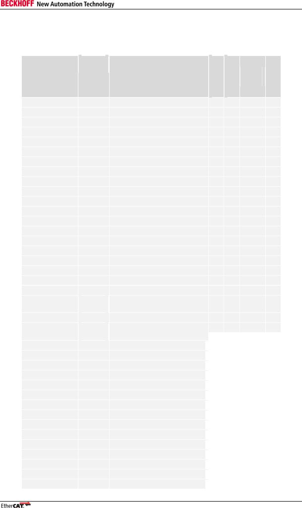
ESC Register Availability
2 ESC Register Availability
Table 2: ESC Register Availability
Address |
Length |
Description |
|
(Byte) |
|
0x0000 |
1 |
Type |
0x0001 |
1 |
Revision |
0x0002:0x0003 |
2 |
Build |
0x0004 |
1 |
FMMUs supported |
0x0005 |
1 |
SyncManagers supported |
0x0006 |
1 |
RAM Size |
0x0007 |
1 |
Port Descriptor |
0x0008:0x0009 |
2 |
ESC Features supported |
0x0010:0x0011 |
2 |
Configured Station Address |
0x0012:0x0013 |
2 |
Configured Station Alias |
0x0020 |
1 |
Write Register Enable |
0x0021 |
1 |
Write Register Protection |
0x0030 |
1 |
ESC Write Enable |
0x0031 |
1 |
ESC Write Protection |
0x0040 |
1 |
ESC Reset ECAT |
0x0041 |
1 |
ESC Reset PDI |
0x0100:0x0101 |
2 |
ESC DL Control |
0x0102:0x0103 |
2 |
Extended ESC DL Control |
0x0108:0x0109 |
2 |
Physical Read/Write Offset |
0x0110:0x0111 |
2 |
ESC DL Status |
0x0120 |
5 bits |
AL Control |
|
[4:0] |
|
0x0120:0x0121 |
2 |
AL Control |
0x0130 |
5 bits |
AL Status |
|
[4:0] |
|
0x0130:0x0131 |
2 |
AL Status |
0x0134:0x0135 |
2 |
AL Status Code |
0x0138 |
1 |
RUN LED Override |
0x0139 |
1 |
ERR LED Override |
0x0140 |
1 |
PDI Control |
0x0141 |
1 |
ESC Configuration |
0x014E:0x014F |
2 |
PDI Information |
0x0150 |
1 |
PDI Configuration |
0x0151 |
1 |
DC Sync/Latch Configuration |
0x0152:0x0153 |
2 |
Extended PDI Configuration |
0x0200:0x0201 |
2 |
ECAT Event Mask |
0x0204:0x0207 |
4 |
PDI AL Event Mask |
0x0210:0x0211 |
2 |
ECAT Event Request |
0x0220:0x0223 |
4 |
AL Event Request |
0x0300:0x0307 |
4x2 |
Rx Error Counter[3:0] |
ET1200 |
ET1100 |
IP Core |
ESC20 |
V3.0.2/ |
|||
V3.00c |
|||
x |
x |
x |
x |
x |
x |
x |
x |
x |
x |
x |
x |
x |
x |
x |
x |
x |
x |
x |
x |
x |
x |
x |
x |
x |
x |
x |
- |
x |
x |
x |
x |
x |
x |
x |
x |
x |
x |
x |
x |
x |
x |
c |
x |
x |
x |
c |
x |
x |
x |
c |
x |
x |
x |
c |
x |
x |
x |
c |
- |
- |
- |
c |
- |
x |
x |
x |
x |
x |
x |
x |
x |
x |
x |
c |
x |
x |
x |
x |
x |
x |
x |
x |
x |
x |
x |
x |
- |
x |
x |
x |
x |
|
|
|
|
|
|
|
|
|
|
|
|
|
|
|
|
|
|
|
|
|
|
|
|
|
|
|
|
|
|
|
|
|
|
|
|
|
x |
|
|
|
x |
|
|
|
x |
|
|
|
- |
|
|
|
|
|
|
|
|
|
|
|
|
|
|
||||
|
|
|
x |
|
|
|
x |
|
|
|
c |
|
|
|
x |
|
|
|
|
|
|
|
|
|
|
|
|
||||||
|
|
|
- |
|
|
|
- |
|
|
|
c |
|
|
|
- |
|
|
|
|
|
|
|
|
|
|
|
|
||||||
|
|
|
- |
|
|
|
- |
|
|
|
c |
|
|
|
- |
|
|
|
|
|
|
|
|
|
|
|
|
|
|
||||
|
|
|
x |
|
|
|
x |
|
|
|
x |
|
|
|
x |
|
|
|
|
|
|
|
|
|
|
|
|
|
|
||||
|
|
|
x |
|
|
|
x |
|
|
|
x |
|
|
|
x |
|
|
|
|
|
|
|
|
|
|
|
|
||||||
|
|
|
- |
|
|
|
- |
|
|
|
c |
|
|
|
- |
|
|
|
|
|
|
|
|
|
|
|
|
|
|
||||
|
|
|
x |
|
|
|
x |
|
|
|
x |
|
|
|
x |
|
|
|
|
|
|
|
|
|
|
|
|
|
|
||||
|
|
|
x |
|
|
|
x |
|
|
|
x |
|
|
|
x |
|
|
|
|
|
|
|
|
|
|
|
|
|
|
||||
|
|
|
x |
|
|
|
x |
|
|
|
x |
|
|
|
x |
|
|
|
|
|
|
|
|
|
|
|
|
|
|
||||
|
|
|
x |
|
|
|
x |
|
|
|
x |
|
|
|
x |
|
|
|
|
|
|
|
|
|
|
|
|
|
|
||||
|
|
|
x |
|
|
|
x |
|
|
|
r/c |
|
|
|
x |
|
|
|
|
|
|
|
|
|
|
|
|
|
|
||||
|
|
|
x |
|
|
|
x |
|
|
|
x |
|
|
|
x |
|
|
|
|
|
|
|
|
|
|
|
|
|
|
||||
|
|
|
x |
|
|
|
x |
|
|
|
x |
|
|
|
x |
|
|
|
|
|
|
|
|
|
|
|
|
|
|
||||
|
|
|
x |
|
|
|
x |
|
|
|
x |
|
|
|
x |
|
Slave Controller – Register Description |
II-7 |

ESC Register Availability
Address |
Length |
Description |
|
(Byte) |
ET1200 |
|
|
ET1100

IP Core
V3.0.2/
V3.00c
 ESC20
ESC20
0x0308:0x030B |
4x1 |
Forwarded Rx Error |
x |
x |
x |
- |
|
|
counter[3:0] |
|
|
|
|
0x030C |
1 |
ECAT Processing Unit Error |
- |
x |
c |
- |
|
|
Counter |
|
|
|
|
0x030D |
1 |
PDI Error Counter |
- |
x |
c |
- |
0x030E |
1 |
PDI Error Code |
- |
- |
c |
- |
0x0310:0x0313 |
4x1 |
Lost Link Counter[3:0] |
x |
x |
c |
x |
0x0400:0x0401 |
2 |
Watchdog Divider |
x |
x |
r/c |
x |
0x0410:0x0411 |
2 |
Watchdog Time PDI |
x |
x |
c |
x |
0x0420:0x0421 |
2 |
Watchdog Time Process Data |
x |
x |
x |
x |
0x0440:0x0441 |
2 |
Watchdog Status Process Data |
x |
x |
x |
x |
0x0442 |
1 |
Watchdog Counter Process |
x |
x |
c |
- |
|
|
Data |
|
|
|
|
0x0443 |
1 |
Watchdog Counter PDI |
x |
x |
c |
- |
0x0500:0x050F |
16 |
SII EEPROM Interface |
x |
x |
x |
x |
0x0510:0x0515 |
6 |
MII Management Interface |
x |
x |
c |
x |
0x0516:0x0517 |
2 |
MII Management Access State |
- |
- |
c |
- |
0x0518:0x051B |
4 |
PHY Port Status[3:0] |
- |
- |
c |
- |
0x0600:0x06FC |
16x13 |
FMMU[15:0] |
3 |
8 |
0-8 |
4 |
0x0800:0x087F |
16x8 |
SyncManager[15:0] |
4 |
8 |
0-8 |
4 |
0x0900:0x090F |
4x4 |
DC – Receive Times[3:0] |
x |
x |
rt |
x |
0x0910:0x0917 |
8 |
DC – System Time |
x |
s/l |
dc |
x |
0x0918:0x091F |
8 |
DC – Receive Time EPU |
x |
s/l |
dc |
x |
0x0920:0x0935 |
24 |
DC – Time Loop Control Unit |
x |
s/l |
dc |
x |
0x0936 |
1 |
DC – Receive Time Latch |
x |
- |
- |
x |
|
|
mode |
|
|
|
|
0x0980 |
1 |
DC – Cyclic Unit Control |
x |
s |
dc |
x |
0x0981 |
1 |
DC – Activation |
x |
s |
dc |
x |
0x0982:0x0983 |
2 |
DC – Pulse length of |
x |
s |
dc |
x |
|
|
SyncSignals |
|
|
|
|
0x0984 |
1 |
DC – Activation Status |
- |
- |
dc |
- |
0x098E:0x09A7 |
26 |
DC – SYNC Out Unit |
x |
s |
dc |
x |
0x09A8 |
1 |
DC – Latch0 Control |
x |
l |
dc |
x |
0x09A9 |
1 |
DC – Latch1 Control |
x |
l |
dc |
x |
0x09AE |
1 |
DC – Latch0 Status |
x |
l |
dc |
x |
0x09B0:0x09B7 |
8 |
DC – Latch0 Positive Edge |
x |
l |
dc |
x |
0x09B8:0x09BF |
8 |
DC – Latch0 Negative Edge |
x |
l |
dc |
x |
0x09C0:0x09C7 |
8 |
DC – Latch1 Positive Edge |
x |
l |
dc |
x |
0x09C7:0x09CF |
8 |
DC – Latch1 Negative Edge |
x |
l |
dc |
x |
0x09F0:0x09F3 |
12 |
DC – SyncManager Event |
- |
s/l |
c |
- |
0x09F8:0x09FF |
|
Times |
|
|
|
|
0x0E00:0x0E03 |
4 |
Power-On Values (Bits) |
8 |
16 |
- |
- |
0x0E00:0x0E07 |
8 |
Product ID |
- |
- |
x |
- |
0x0E08:0x0E0F |
8 |
Vendor ID |
- |
- |
x |
- |
II-8 |
Slave Controller – Register Description |
ESC Register Availability
Address |
Length |
Description |
|
(Byte) |
ET1200 |
|
|
ET1100

IP Core
V3.0.2/
V3.00c
 ESC20
ESC20
|
0x0F00:0x0F03 |
|
|
|
4 |
|
|
|
Digital I/O Output Data |
|
|
|
|
x |
|
|
|
x |
|
|
|
|
io |
|
|
|
x |
|
|
|
|
|
|
|
|
|
|
|
|
|
|||||||||||||||||
|
0x0F10:0x0F17 |
|
|
|
8 |
|
|
|
General Purpose Outputs |
|
|
|
2 |
|
|
|
2 |
|
|
|
0-8 |
|
|
|
- |
|
||
|
|
|
|
|
|
|
|
|
[Byte] |
|
|
|
|
|
|
|
|
|
|
|
|
|
|
|
|
|
|
|
|
|
|
|
|
|
|
|
|
|
|
|
|||||||||||||||||
|
0x0F18:0x0F1F |
|
|
|
8 |
|
|
|
General Purpose Inputs [Byte] |
|
|
|
- |
|
|
|
2 |
|
|
|
0-8 |
|
|
|
- |
|
||
|
|
|
|
|
|
|
|
|
|
|
|
|
|
|
|
|
|
|
|
|
|
|
|
|
|
|||
|
0x0F80:0x0FFF |
|
|
|
128 |
|
|
|
User RAM |
|
|
|
|
x |
|
|
|
x |
|
|
|
|
x |
|
|
|
x |
|
|
|
|
|
|
|
|
|
|
|
|
|
|
|
|
|
|
|
|
|
|
|
|
|
|
|
|||
|
0x1000:0x1003 |
|
|
|
4 |
|
|
|
Digital I/O Input Data |
|
|
|
|
io |
|
|
|
io |
|
|
|
|
io |
|
|
|
io |
|
|
|
|
|
|
|
|
|
|
|
|
|
|
|
|
||||||||||||||
|
0x1000 ff. |
|
|
|
|
|
|
|
Process Data RAM [Kbyte] |
|
|
|
1 |
|
|
|
8 |
|
|
|
0-60 |
|
|
|
4 |
|
||
|
|
Table 3: ESC Register Availability Legend |
|
|||
|
|
|
|
|
|
|
|
Symbol |
|
|
|
Description |
|
|
|
|
|
|
|
|
|
x |
|
|
|
Available |
|
|
|
|
|
|
|
|
|
- |
|
|
|
Not available |
|
|
|
|
|
|
|
|
|
r |
|
|
|
Read only |
|
|
|
|
|
|
|
|
|
c |
|
|
|
Configurable |
|
|
|
|
|
|
|
|
|
dc |
|
|
|
Available if Distributed Clocks with all |
|
|
|
|
|
|
Sync/Latch signals are enabled |
|
|
|
|
|
|
|
|
|
|
|
|
|
|
|
|
rt |
|
|
|
Available if Receive Times or Distributed Clocks |
|
|
|
|
|
|
are enabled (always available for 3-4 ports) |
|
|
|
|
|
|
|
|
|
s |
|
|
|
Available if DC SYNC Out Unit enabled |
|
|
|
|
|
|
(Register 0x0140.10=1) |
|
|
|
|
|
|
|
|
|
|
|
|
|
|
|
|
l |
|
|
|
Available if DC Latch In Unit enabled |
|
|
|
|
|
|
(Register 0x0140.11=1) |
|
|
|
|
|
|
|
|
|
|
|
|
|
|
|
|
|
|
|
|
|
|
|
s/l |
|
|
|
Available if DC SYNC Out Unit enabled and/or |
|
|
|
|
|
|
DC Latch In Unit enabled |
|
|
|
|
|
|
(Register 0x0140.10=1 and/or 0x0140.11=1) |
|
|
|
|
|
|
|
|
|
io |
|
|
|
Available if Digital I/O PDI is selected |
|
|
|
|
|
|
|
|
Slave Controller – Register Description |
II-9 |

Type (0x0000)
3 Register description
3.1Type (0x0000)
Table 4: Register Type (0x0000)
|
ESC20 |
|
ET1100 |
|
ET1200 |
|
IP Core |
|
||||
|
|
|
|
|
||||||||
|
|
|
|
|
|
|
|
|
|
|
|
|
|
Bit |
|
|
|
Description |
|
|
|
ECAT |
|
|
|
PDI |
|
|
|
Reset Value |
|
|
|
|
|
|
|
|
|
|
|
|
|
|
|
|
|
|
|
|
|
|
|
|
|
7:0 |
|
|
|
Type of EtherCAT controller |
|
|
|
r/- |
|
|
|
r/- |
|
|
|
Beckhoff: |
|
|
|
|
|
|
|
|
|
|
|
|
|
|
|
|
|
|
|
|
First terminals : |
0x01 |
|
|
|
|
|
|
|
|
|
|
|
|
|
|
|
|
|
|
|||||
|
|
|
|
|
|
|
|
|
|
|
|
|
|
|
|
|
ESC10, ESC20: |
0x02 |
|
|
|
|
|
|
|
|
|
|
|
|
|
|
|
|
|
|
|
First EK1100: |
|
0x03 |
|
|
|
|
|
|
|
|
|
|
|
|
|
|
|
|
|
|
IP Core: |
|
0x04 |
|
|
|
|
|
|
|
|
|
|
|
|
|
|
|
|
|
|
Terminals: |
|
0x05 |
|
|
|
|
|
|
|
|
|
|
|
|
|
|
|
|
|
|
ET1100: |
|
0x11 |
|
|
|
|
|
|
|
|
|
|
|
|
|
|
|
|
|
|
ET1200: |
|
0x12 |
|
|
|
|
|
|
|
|
|
|
|
|
|
|
|
|
|
|
Other vendors: |
|
|
|
|
|
|
|
|
|
|
|
|
|
|
|
|
|
|
|
|
Hilscher: |
0x80-0x88 |
|
|
|
|
|
|
|
|
|
|
|
|
|
|
|
|
|
|
|
|
|
|
|
|
|
|
|
|
|
|
|
|
|
|
|
|
|
|
|
|
TI: |
|
0x90 |
|
|
|
|
|
|
|
|
|
|
|
|
|
|
|
|
|
|
Test: |
|
0xEE |
|
|
|
|
|
|
|
|
|
|
|
|
|
|
|
|
|
|
|
|
|
|
3.2Revision (0x0001)
Table 5: Register Revision (0x0001)
|
|
|
|
|
|
|
|
|
|
|
ESC20 |
|
ET1100 |
|
ET1200 |
|
IP Core |
|
|||||||
|
|
|
|
|
|
|
|
|
|
|
|
|
|
|
|||||||||||
|
|
|
|
|
|
|
|
|
|
|
|
|
|
|
|
|
|
|
|
||||||
|
Bit |
|
|
|
Description |
|
|
|
ECAT |
|
|
|
PDI |
|
|
|
Reset Value |
|
|
||||||
|
|
|
|
|
|
|
|
|
|
|
|
|
|
|
|
|
|
||||||||
|
7:0 |
|
|
|
Revision of EtherCAT controller. |
|
|
|
r/- |
|
|
|
r/- |
|
|
|
ESC dep. |
|
|
||||||
|
|
|
|
|
IP Core: major version X |
|
|
|
|
|
|
|
|
|
|
|
|
|
|
|
|
|
|
|
|
|
|
|
|
|
|
|
|
|
|
|
|
|
|
|
|
|
|
|
|
|
|
|
|
|
|
|
|
|
|
|
|
|
|
|
|
|
|
|
|
|
|
|
|
|
|
|
|
|
|
|
|
|
|
|
|
|
|
|
|
|
|
|
|
|
|
|
|
|
|
|
|
|
|
|
|
|
|
3.3Build (0x0002:0x0003)
Table 6: Register Build (0x0002:0x0003)
|
|
|
|
|
|
|
|
|
|
|
ESC20 |
|
ET1100 |
|
ET1200 |
|
IP Core |
|
|||||||
|
|
|
|
|
|
|
|
|
|
|
|
|
|
|
|||||||||||
|
|
|
|
|
|
|
|
|
|
|
|
|
|
|
|
|
|
|
|
||||||
|
Bit |
|
|
|
Description |
|
|
|
ECAT |
|
|
|
PDI |
|
|
|
Reset Value |
|
|
||||||
|
|
|
|
|
|
|
|
|
|
|
|
|
|
|
|
|
|
||||||||
|
15:0 |
|
|
|
Actual build of EtherCAT controller. |
|
|
|
r/- |
|
|
|
r/- |
|
|
|
ESC dep. |
|
|
||||||
|
|
|
|
|
IP Core: [7:4] = minor version Y, |
|
|
|
|
|
|
|
|
|
|
|
|
|
|
|
|
|
|
|
|
|
|
|
|
|
|
|
|
|
|
|
|
|
|
|
|
|
|
|
|
|
|
|
|
|
|
|
|
|
|
|
|
|
|
|
|
|
|
|
|
|
|
|
|
|
|
|
|
|
|
|
|
|
|
|
|
|
[3:0] = maintenance version Z |
|
|
|
|
|
|
|
|
|
|
|
|
|
|
|
|
|
|
|
|
3.4FMMUs supported (0x0004)
Table 7: Register FMMUs supported (0x0004)
|
|
|
|
|
|
|
|
ESC20 |
|
ET1100 |
|
ET1200 |
|
IP Core |
|
||||||
|
|
|
|
|
|
|
|
|
|
|
|
||||||||||
|
|
|
|
|
|
|
|
|
|
|
|
|
|
|
|
||||||
Bit |
|
|
Description |
|
|
ECAT |
|
|
PDI |
|
|
|
Reset Value |
|
|
||||||
|
|
|
|
|
|
|
|
|
|
|
|
|
|
|
|||||||
7:0 |
|
|
Number of supported FMMU channels (or |
|
|
r/- |
|
|
r/- |
|
|
|
ESC20: 4 |
|
|
||||||
|
|
|
entities) of the EtherCAT Slave Controller. |
|
|
|
|
|
|
|
|
|
|
|
IP Core: depends on |
|
|
||||
|
|
|
|
|
|
|
|
|
|
|
|
|
|
|
|||||||
|
|
|
|
|
|
|
|
|
|
|
|
|
|
configuration |
|
|
|||||
|
|
|
|
|
|
|
|
|
|
|
|
|
|
|
|
|
|||||
|
|
|
|
|
|
|
|
|
|
|
|
|
|
|
ET1100: 8 |
|
|
||||
|
|
|
|
|
|
|
|
|
|
|
|
|
|
|
ET1200: 3 |
|
|
||||
|
|
|
|
|
|
|
|
|
|
|
|
|
|
|
|
|
|
|
|
|
|
II-10 |
Slave Controller – Register Description |

SyncManagers supported (0x0005)
3.5SyncManagers supported (0x0005)
Table 8: Register SyncManagers supported (0x0005)
|
|
|
|
|
|
|
|
|
|
|
ESC20 |
|
ET1100 |
|
ET1200 |
|
IP Core |
|
|||||||
|
|
|
|
|
|
|
|
|
|
|
|
|
|
|
|||||||||||
|
|
|
|
|
|
|
|
|
|
|
|
|
|
|
|
|
|
|
|
||||||
|
Bit |
|
|
|
Description |
|
|
|
ECAT |
|
|
|
PDI |
|
|
|
Reset Value |
|
|
||||||
|
|
|
|
|
|
|
|
|
|
|
|
|
|
|
|
|
|
||||||||
|
7:0 |
|
|
|
Number of supported SyncManager channels |
|
|
|
r/- |
|
|
|
r/- |
|
|
|
ESC20: 4 |
|
|
||||||
|
|
|
|
|
(or entities) of the EtherCAT Slave Controller |
|
|
|
|
|
|
|
|
|
|
|
|
|
IP Core: depends on |
|
|
||||
|
|
|
|
|
|
|
|
|
|
|
|
|
|
|
|
|
|
|
|||||||
|
|
|
|
|
|
|
|
|
|
|
|
|
|
|
|
|
|
configuration |
|
|
|||||
|
|
|
|
|
|
|
|
|
|
|
|
|
|
|
|
|
|
|
|
|
|||||
|
|
|
|
|
|
|
|
|
|
|
|
|
|
|
|
|
|
|
ET1100: 8 |
|
|
||||
|
|
|
|
|
|
|
|
|
|
|
|
|
|
|
|
|
|
|
ET1200: 4 |
|
|
||||
3.6RAM Size (0x0006)
Table 9: Register RAM Size (0x0006)
|
|
|
|
|
|
|
|
|
|
|
ESC20 |
|
ET1100 |
|
ET1200 |
|
IP Core |
|
|||||||
|
|
|
|
|
|
|
|
|
|
|
|
|
|
|
|||||||||||
|
|
|
|
|
|
|
|
|
|
|
|
|
|
|
|
|
|
|
|
||||||
|
Bit |
|
|
|
Description |
|
|
|
ECAT |
|
|
|
PDI |
|
|
|
Reset Value |
|
|
||||||
|
|
|
|
|
|
|
|
|
|
|
|
|
|
|
|
|
|
||||||||
|
7:0 |
|
|
|
Process Data RAM size supported by the |
|
|
|
r/- |
|
|
|
r/- |
|
|
|
ESC20: 4 |
|
|
||||||
|
|
|
|
|
EtherCAT Slave Controller in KByte |
|
|
|
|
|
|
|
|
|
|
|
|
|
IP Core: depends on |
|
|
||||
|
|
|
|
|
|
|
|
|
|
|
|
|
|
|
|
|
|
|
|||||||
|
|
|
|
|
|
|
|
|
|
|
|
|
|
|
|
|
|
configuration |
|
|
|||||
|
|
|
|
|
|
|
|
|
|
|
|
|
|
|
|
|
|
|
|
|
|||||
|
|
|
|
|
|
|
|
|
|
|
|
|
|
|
|
|
|
|
ET1100: 8 |
|
|
||||
|
|
|
|
|
|
|
|
|
|
|
|
|
|
|
|
|
|
|
ET1200: 1 |
|
|
||||
3.7Port Descriptor (0x0007)
Table 10: Register Port Descriptor (0x0007)
|
|
|
|
|
|
|
|
|
|
|
ESC20 |
|
ET1100 |
|
ET1200 |
|
IP Core |
|
|||||||
|
|
|
|
|
|
|
|
|
|
|
|
|
|
|
|||||||||||
|
|
|
|
|
|
|
|
|
|
|
|
|
|
|
|
|
|
|
|
||||||
|
Bit |
|
|
|
Description |
|
|
|
ECAT |
|
|
|
PDI |
|
|
|
Reset Value |
|
|
||||||
|
|
|
|
|
|
|
|
|
|
|
|
|
|
|
|
|
|
|
|
|
|
|
|
|
|
Port configuration: 00: Not implemented
01: Not configured (SII EEPROM)
10:EBUS
11:MII / RMII / RGMII
|
1:0 |
|
|
|
Port 0 |
|
|
|
r/- |
|
|
|
r/- |
|
|
|
ESC and ESC |
|
|
|
|
|
|
|
|
|
|
|
|
|
|
|
|||||
|
|
|
|
|
|
|
|
|
|
|
|
|
configuration dep. |
|
||||
|
|
|
|
|
|
|
|
|
|
|
|
|
|
|
|
|
|
|
|
3:2 |
|
|
|
Port 1 |
|
|
|
r/- |
|
|
|
r/- |
|
|
|
|
|
|
|
|
|
|
|
|
|
|
|
|
|
|
|
|
||||
|
|
|
|
|
|
|
|
|
|
|
|
|
|
|
|
|
|
|
|
5:4 |
|
|
|
Port 2 |
|
|
|
r/- |
|
|
|
r/- |
|
|
|
|
|
|
|
|
|
|
|
|
|
|
|
|
|
|
|
|
|
|
|
|
|
7:6 |
|
|
|
Port 3 |
|
|
|
r/- |
|
|
|
r/- |
|
|
|
|
|
Slave Controller – Register Description |
II-11 |

ESC Features supported (0x0008:0x0009)
3.8ESC Features supported (0x0008:0x0009)
Table 11: Register ESC Features supported (0x0008:0x0009)
ESC20 |
|
ET1100 |
|
ET1200 |
|
IP Core |
|
|
|
[8] |
V2.2.0/ |
V2.02a |
|
|
Bit |
|
|
|
Description |
|
|
|
ECAT |
|
|
|
PDI |
|
|
|
Reset Value |
|
|
|
|
|
|
|
|
|
|
|
|
|
|
|
|
|
|
|
||||||
|
|
0 |
|
|
|
FMMU Operation: |
|
|
|
r/- |
|
|
|
r/- |
|
|
|
0 |
|
|
|
|
|
|
|
|
0: |
Bit oriented |
|
|
|
|
|
|
|
|
|
|
|
|
|
|
|
|
|
|
|
|
|
1: |
Byte oriented |
|
|
|
|
|
|
|
|
|
|
|
|
|
|
|
|
|
|
|
|
|
|
|
|
|
|
|
|
|
|
||||||
|
|
1 |
|
|
|
Reserved |
|
|
|
r/- |
|
|
|
r/- |
|
|
|
0 |
|
|
|
|
|
|
|
|
|
|
|
|
|
|
|
|
|
|
|
|
|||||
|
|
2 |
|
|
|
Distributed Clocks: |
|
|
|
r/- |
|
|
|
r/- |
|
|
|
ESC20: 1 |
|
|
|
|
|
|
|
|
|
0: |
Not available |
|
|
|
|
|
|
|
|
|
|
|
IP Core: depends on |
|
|
|
|
|
|
|
|
|
|
|
|
|
|
|
|
|
|
|
configuration |
|
|
||
|
|
|
|
|
|
1: |
Available |
|
|
|
|
|
|
|
|
|
|
|
|
|
|
|
|
|
|
|
|
|
|
|
|
|
|
|
|
|
|
|
ET1100: 1 |
|
|
||
|
|
|
|
|
|
|
|
|
|
|
|
|
|
|
|
|
|
|
|
|
|
|
|
|
|
|
|
|
|
|
|
|
|
|
|
|
|
|
|
|
|
|
|
|
|
|
|
|
|
|
|
|
|
|
|
|
|
|
|
|
|
|
ET1200: 1 |
|
|
|
|
|
|
|
|
|
|
|
|
|
|
|
|
|
|
|
|||||
|
|
3 |
|
|
|
Distributed Clocks (width): |
|
|
|
r/- |
|
|
|
r/- |
|
|
|
ET1100: 1 |
|
|
|
|
|
|
|
|
|
0: |
32 bit |
|
|
|
|
|
|
|
|
|
|
|
ET1200: 1 |
|
|
|
|
|
|
|
|
|
|
|
|
|
|
|
|
|
|
|
|||||
|
|
|
|
|
|
|
|
|
|
|
|
|
|
|
|
|
IP Core: depends on |
|
|
||
|
|
|
|
|
|
1: |
64 bit |
|
|
|
|
|
|
|
|
|
|
|
|
|
|
|
|
|
|
|
|
|
|
|
|
|
|
|
|
|
|
|
configuration |
|
|
||
|
|
|
|
|
|
|
|
|
|
|
|
|
|
|
|
|
|
|
|
|
|
|
|
|
|
|
|
|
|
|
|
|
|
|
|
|
|
|
|
|
Others : 0 |
|
|
|
|
|
|
|
|
|
|
|
|
|
|
|
|
|
|
|
|||||
|
|
4 |
|
|
|
Low Jitter EBUS: |
|
|
|
r/- |
|
|
|
r/- |
|
|
|
ET1100: 1 |
|
|
|
|
|
|
|
|
|
0: |
Not available, standard jitter |
|
|
|
|
|
|
|
|
|
|
|
ET1200: 1 |
|
|
|
|
|
|
|
|
|
|
|
|
|
|
|
|
|
|
|
|||||
|
|
|
|
|
|
|
|
|
|
|
|
|
|
|
|
|
Others : 0 |
|
|
||
|
|
|
|
|
|
1: |
Available, jitter minimized |
|
|
|
|
|
|
|
|
|
|
|
|
|
|
|
|
|
|
|
|
|
|
|
|
|
|
|
|
|
|
|
|
|
|
||
|
|
|
|
|
|
|
|
|
|
|
|
|
|
|
|
|
|||||
|
|
5 |
|
|
|
Enhanced Link Detection EBUS: |
|
|
|
r/- |
|
|
|
r/- |
|
|
|
ET1100: 1 |
|
|
|
|
|
|
|
|
|
0: |
Not available |
|
|
|
|
|
|
|
|
|
|
|
ET1200: 1 |
|
|
|
|
|
|
|
|
|
|
|
|
|
|
|
|
|
|
|
|||||
|
|
|
|
|
|
|
|
|
|
|
|
|
|
|
|
|
Others : 0 |
|
|
||
|
|
|
|
|
|
1: |
Available |
|
|
|
|
|
|
|
|
|
|
|
|
|
|
|
|
|
|
|
|
|
|
|
|
|
|
|
|
|
|
|
|
|
|
||
|
|
|
|
|
|
|
|
|
|
|
|
|
|
|
|
|
|||||
|
|
6 |
|
|
|
Enhanced Link Detection MII: |
|
|
|
r/- |
|
|
|
r/- |
|
|
|
ET1100: 1 |
|
|
|
|
|
|
|
|
|
0: |
Not available |
|
|
|
|
|
|
|
|
|
|
|
ET1200: 1 |
|
|
|
|
|
|
|
|
|
|
|
|
|
|
|
|
|
|
|
|||||
|
|
|
|
|
|
|
|
|
|
|
|
|
|
|
|
|
Others : 0 |
|
|
||
|
|
|
|
|
|
1: |
Available |
|
|
|
|
|
|
|
|
|
|
|
|
|
|
|
|
|
|
|
|
|
|
|
|
|
|
|
|
|
|
|
|
|
|
||
|
|
|
|
|
|
|
|
|
|
|
|
|
|
|
|
|
|||||
|
|
7 |
|
|
|
Separate Handling of FCS Errors: |
|
|
|
r/- |
|
|
|
r/- |
|
|
|
IP Core: 1 |
|
|
|
|
|
|
|
|
|
0: |
Not supported |
|
|
|
|
|
|
|
|
|
|
|
ET1100: 1 |
|
|
|
|
|
|
|
|
|
|
|
|
|
|
|
|
|
|
|
|||||
|
|
|
|
|
|
|
|
|
|
|
|
|
|
|
|
|
ET1200: 1 |
|
|
||
|
|
|
|
|
|
1: |
Supported, frames with wrong FCS and |
|
|
|
|
|
|
|
|
|
|
|
|
|
|
|
|
|
|
|
|
|
|
|
|
|
|
|
|
|
|
|
Others : 0 |
|
|
||
|
|
|
|
|
|
|
additional nibble will be counted |
|
|
|
|
|
|
|
|
|
|
|
|
|
|
|
|
|
|
|
|
|
|
|
|
|
|
|
|
|
|
|
|
|
|
|
|
|
|
|
|
|
|
|
separately in Forwarded RX Error |
|
|
|
|
|
|
|
|
|
|
|
|
|
|
|
|
|
|
|
|
|
Counter |
|
|
|
|
|
|
|
|
|
|
|
|
|
|
|
|
|
|
|
|
|
|
|
|
|
|
|
|
|
|
|
|||||
|
|
8 |
|
|
|
Enhanced DC SYNC Activation |
|
|
|
r/- |
|
|
|
r/- |
|
|
|
IP Core: |
|
|
|
|
|
|
|
|
|
|
|
|
|
|
|
|
|
depends on version |
|
|
|||||
|
|
|
|
|
|
0: |
Not available |
|
|
|
|
|
|
|
|
|
|
|
|
|
|
|
|
|
|
|
|
|
|
|
|
|
|
|
|
|
|
|
|||||
|
|
|
|
|
|
|
|
|
|
|
|
|
|
|
|
|
Others : 0 |
|
|
||
|
|
|
|
|
|
1: |
Available |
|
|
|
|
|
|
|
|
|
|
|
|
|
|
|
|
|
|
|
|
|
|
|
|
|
|
|
|
|
|
|
|
|
|
||
|
|
|
|
|
|
NOTE: This feature refers to registers 0x981[7:3], |
|
|
|
|
|
|
|
|
|
|
|
|
|
|
|
|
|
|
|
|
|
0x0984 |
|
|
|
|
|
|
|
|
|
|
|
|
|
|
|
|
|
|
|
|
|
|
|
|
|
|
|
|
|
|
|
|
|
|
|||
|
|
|
|
|
|
|
|
|
|
|
|
|
|
|
|
||||||
|
|
9 |
|
|
|
EtherCAT LRW command support: |
|
|
|
r/- |
|
|
|
r/- |
|
|
|
0 |
|
|
|
|
|
|
|
|
0: |
Supported |
|
|
|
|
|
|
|
|
|
|
|
|
|
|
|
|
|
|
|
|
|
1: |
Not supported |
|
|
|
|
|
|
|
|
|
|
|
|
|
|
|
|
|
|
|
|
|
|
|
|
|
|
|
|
|
|
||||||
|
|
10 |
|
|
|
EtherCAT read/write command support |
|
|
|
r/- |
|
|
|
r/- |
|
|
|
0 |
|
|
|
|
|
|
|
|
|
(BRW, APRW, FPRW): |
|
|
|
|
|
|
|
|
|
|
|
|
|
|
|
|
|
|
|
|
|
0: |
Supported |
|
|
|
|
|
|
|
|
|
|
|
|
|
|
|
|
|
|
|
|
1: |
Not supported |
|
|
|
|
|
|
|
|
|
|
|
|
|
|
|
|
|
|
|
|
|
|
|
|
|
|
|
|
|
|
||||||
|
|
11 |
|
|
|
Fixed FMMU/SyncManager configuration |
|
|
|
r/- |
|
|
|
r/- |
|
|
|
0 |
|
|
|
|
|
|
|
|
|
0: |
Variable configuration |
|
|
|
|
|
|
|
|
|
|
|
|
|
|
|
|
|
|
|
|
|
|
|
|
|
|
|
|
|
|
|
|
|
|||
|
|
|
|
|
|
1: |
Fixed configuration (refer to |
|
|
|
|
|
|
|
|
|
|
|
|
|
|
|
|
|
|
|
|
|
documentation of supporting ESCs) |
|
|
|
|
|
|
|
|
|
|
|
|
|
|
|
|
|
|
|
|
|
|
|
|
|
|
|
|
|
|
||||||
|
|
15:12 |
|
|
|
Reserved |
|
|
|
r/- |
|
|
|
r/- |
|
|
|
0 |
|
|
|
|
|
|
|
|
|
|
|
|
|
|
|
|
|
|
|
|
|
|
|
|
|
II-12 |
|
|
|
|
|
|
|
|
Slave Controller – Register Description |
||||||||||||
Configured Station Address (0x0010:0x0011)
3.9Configured Station Address (0x0010:0x0011)
Table 12: Register Configured Station Address (0x0010:0x0011)
|
ESC20 |
|
ET1100 |
|
ET1200 |
|
IP Core |
|
||||
|
|
|
|
|
||||||||
|
|
|
|
|
|
|
|
|
|
|
|
|
|
Bit |
|
|
|
Description |
|
|
|
ECAT |
|
|
|
PDI |
|
|
|
Reset Value |
|
|
||||||
|
|
|
|
|
|
|
|
|
|
|
|
|
|
|
|
|
|
|
|
|
|
|
|
|
|
|
15:0 |
|
|
|
Address used for node addressing (FPxx |
|
|
|
r/w |
|
|
|
r/- |
|
|
|
0 |
|
|
|
|
|
|
||
|
|
|
|
|
commands) |
|
|
|
|
|
|
|
|
|
|
|
|
|
|
|
|
|
|
|
|
3.10 Configured Station Alias (0x0012:0x0013) |
|
|
|
|
|
|
|
|
|
|
|
|
|
|
|
|
|
|
|
|
|||||
|
|
|
|
|
Table 13: Register Configured Station Alias (0x0012:0x0013) |
|
|
||||||||||||||||||
|
|
|
|
|
|
|
|
|
|
|
|
|
|
|
|
|
|
|
|
||||||
|
|
|
|
|
|
|
|
|
|
|
ESC20 |
|
ET1100 |
|
ET1200 |
|
IP Core |
|
|
||||||
|
|
|
|
|
|
|
|
|
|
|
|
|
|
|
|
|
|
|
|
||||||
|
Bit |
|
|
|
Description |
|
|
|
ECAT |
|
|
|
PDI |
|
|
|
Reset Value |
|
|
||||||
|
|
|
|
|
|
|
|
|
|
|
|
|
|
|
|
|
|
|
|||||||
|
15:0 |
|
|
|
Alias Address used for node addressing |
|
|
|
r/- |
|
|
|
r/w |
|
|
|
0 until first EEPROM |
|
|
||||||
|
|
|
|
|
|
|
|
|
|
|
|
|
load, then EEPROM |
|
|
||||||||||
|
|
|
|
|
(FPxx commands). |
|
|
|
|
|
|
|
|
|
|
|
|
|
|
|
|||||
|
|
|
|
|
|
|
|
|
|
|
|
|
|
|
|
|
|
ADR 0x0004 |
|
|
|||||
|
|
|
|
|
The use of this alias is activated by Register |
|
|
|
|
|
|
|
|
|
|
|
|
|
|
|
|||||
|
|
|
|
|
|
|
|
|
|
|
|
|
|
|
|
|
|
|
|
|
|
|
|
|
|
|
|
|
|
|
DL Control Bit 24 (0x0100.24/0x0103.0) |
|
|
|
|
|
|
|
|
|
|
|
|
|
|
|
|
|
|
|
|
|
|
|
|
|
|
|
|
|
|
|
|
|
|
|
|
|
|
|
|
|
|
|
|
|
|
NOTE: EEPROM value is only taken over at first
EEPROM load after power-on or reset.
ESC20 exception: EEPROM value is taken over after each EEPROM reload command.
3.11 Write Register Enable (0x0020)
Table 14: Register Write Register Enable (0x0020)
ESC20 |
|
ET1100 |
|
ET1200 |
|
IP Core |
|
|
|
read |
read: |
|
V2.4.0/ |
|
V2.04a |
|
Bit |
|
|
|
Description |
|
|
|
ECAT |
|
|
|
PDI |
|
|
|
Reset Value |
|
|
|
|
|
|
|
|
|
|
|
|
|
|
|
|
||||
|
0 |
|
|
|
If write register protection is enabled, this |
|
|
|
r/w |
|
|
|
r/- |
|
|
|
0 |
|
|
|
|
|
|
register has to be written in the same |
|
|
|
|
|
|
|
|
|
|
|
|
|
|
|
|
|
|
Ethernet frame (value does not care) before |
|
|
|
|
|
|
|
|
|
|
|
|
|
|
|
|
|
|
other writes to this station are allowed. Write |
|
|
|
|
|
|
|
|
|
|
|
|
|
|
|
|
|
|
protection is still active after this frame (if |
|
|
|
|
|
|
|
|
|
|
|
|
|
|
|
|
|
|
Write Register Protection register is not |
|
|
|
|
|
|
|
|
|
|
|
|
|
|
|
|
|
|
changed). |
|
|
|
|
|
|
|
|
|
|
|
|
|
|
|
|
|
|
|
|
|
|
|
|
|
|
|
|
||||
|
7:1 |
|
|
|
Reserved, write 0 |
|
|
|
r/- |
|
|
|
r/- |
|
|
|
0 |
|
3.12 Write Register Protection (0x0021)
Table 15: Register Write Register Protection (0x0021)
ESC20 |
|
ET1100 |
|
ET1200 |
|
IP Core |
|
|
|
Bit |
Description |
0 Write register protection:
0:Protection disabled
1:Protection enabled
Registers 0x0000-0x0137, 0x013A-0x0F0F are write protected, except for 0x0030.
7:1 |
Reserved, write 0 |
|
|
|
ECAT |
|
|
|
PDI |
|
|
|
Reset Value |
|
|
|
|
|
|
|
|
|
|
|
|||
|
|
|
r/w |
|
|
|
r/- |
|
|
|
0 |
|
|
|
|
|
|
|
|
|
|
|
|
|
|
|
|
|
|
|
|
|
|
|
|
|
|
|
|
|
|
|
|
|
|
|
|
|
|
|
|
|
|
|
r/- |
|
|
|
r/- |
|
|
|
0 |
|
|
|
|
|
|
|
|
|
|
|
|||
|
|
|
|
|
|
|
|
|
|
|
|
|
Slave Controller – Register Description |
II-13 |

ESC Write Enable (0x0030)
3.13 ESC Write Enable (0x0030)
Table 16: Register ESC Write Enable (0x0030)
ESC20 |
|
ET1100 |
|
ET1200 |
|
IP Core |
|
|
|
read |
read: |
|
V2.4.0/ |
|
V2.04a |
|
Bit |
|
|
|
Description |
|
|
|
ECAT |
|
|
|
PDI |
|
|
|
Reset Value |
|
|
||||||||
|
|
|
|
|
|
|
|
|
|
|
|
|
|
|
|
|
|
|
|
|
|
|
|||||
|
0 |
|
|
|
If ESC write protection is enabled, this |
|
|
|
r/w |
|
|
|
r/- |
|
|
|
0 |
|
|
|
|
|
|
||||
|
|
|
|
|
register has to be written in the same |
|
|
|
|
|
|
|
|
|
|
|
|
|
|
|
|
|
|
|
|
|
|
|
|
|
|
|
Ethernet frame (value does not care) before |
|
|
|
|
|
|
|
|
|
|
|
|
|
|
|
|
|
|
|
|
|
|
|
|
|
|
|
other writes to this station are allowed. ESC |
|
|
|
|
|
|
|
|
|
|
|
|
|
|
|
|
|
|
|
|
|
|
|
|
|
|
|
write protection is still active after this frame |
|
|
|
|
|
|
|
|
|
|
|
|
|
|
|
|
|
|
|
|
|
|
|
|
|
|
|
(if ESC Write Protection register is not |
|
|
|
|
|
|
|
|
|
|
|
|
|
|
|
|
|
|
|
|
|
|
|
|
|
|
|
changed). |
|
|
|
|
|
|
|
|
|
|
|
|
|
|
|
|
|
|
|
|
|
|
|
|
|
|
|
|
|
|
|
|
|
|
|
|
|
|
|
|
|
|
|
|
|
|||||
|
7:1 |
|
|
|
Reserved, write 0 |
|
|
|
r/- |
|
|
|
r/- |
|
|
|
0 |
|
|
|
|
|
|
||||
3.14 ESC Write Protection (0x0031) |
|
|
|
|
|
|
|
|
|
|
|
|
|
|
|
|
|
|
|
|
|
||||||
|
|
|
|
|
|
Table 17: Register ESC Write Protection (0x0031) |
|
|
|
|
|
|
|
|
|
|
|||||||||||
|
|
|
|
|
|
|
|
|
|
|
|
|
|
|
|
|
|
|
|
|
|
||||||
|
|
|
|
|
|
|
|
|
|
|
|
ESC20 |
|
|
ET1100 |
|
ET1200 |
|
IP Core |
|
|
||||||
|
|
|
|
|
|
|
|
|
|
|
|
|
|
|
|
|
|
|
|
||||||||
|
Bit |
|
|
|
Description |
|
|
|
ECAT |
|
|
|
PDI |
|
|
|
Reset Value |
|
|
||||||||
|
|
|
|
|
|
|
|
|
|
|
|
|
|
|
|
|
|
|
|
||||||||
|
0 |
|
|
|
Write protect: |
|
|
|
r/w |
|
|
|
r/- |
|
|
|
0 |
|
|
|
|
|
|
||||
|
|
|
|
|
0: |
Protection disabled |
|
|
|
|
|
|
|
|
|
|
|
|
|
|
|
|
|
|
|
|
|
|
|
|
|
|
|
|
|
|
|
|
|
|
|
|
|
|
|
|
|
|
|
|
|
|
|||
|
|
|
|
|
1: |
Protection enabled |
|
|
|
|
|
|
|
|
|
|
|
|
|
|
|
|
|
|
|
|
|
|
|
|
|
|
All areas are write protected, except for 0x0030. |
|
|
|
|
|
|
|
|
|
|
|
|
|
|
|
|
|
|
|
|
|
|
|
|
|
|
|
|
|
|
|
|
|
|
|
|
|
|
|
|
|
|
|
|
||||||
|
|
|
|
|
|
|
|
|
|
|
|
|
|
|
|
|
|
|
|
||||||||
|
7:1 |
|
|
|
Reserved, write 0 |
|
|
|
r/- |
|
|
|
r/- |
|
|
|
0 |
|
|
|
|
|
|
||||
|
|
|
|
|
|
|
|
|
|
|
|
|
|
|
|
|
|
|
|
|
|
|
|
|
|
|
|
II-14 |
Slave Controller – Register Description |

|
|
|
|
|
|
|
|
|
|
|
|
|
|
|
|
|
ESC Reset ECAT (0x0040) |
|||||||||
3.15 ESC Reset ECAT (0x0040) |
|
|
|
|
|
|
|
|
|
|
|
|
|
|
|
|
|
|
|
|
||||||
|
|
|
|
|
|
Table 18: Register ESC Reset ECAT (0x0040) |
|
|
|
|
|
|
|
|
|
|
||||||||||
|
|
|
|
|
|
|
|
|
|
|
|
|
|
|
|
|
|
|
|
|
|
|
|
|
|
|
|
|
|
|
|
|
|
|
|
|
|
|
ESC20 |
|
ET1100 |
|
ET1200 |
|
IP Core |
|
|||||||
|
|
|
|
|
|
|
|
|
|
|
|
|
|
|
|
|
|
|
|
|
||||||
|
|
Bit |
|
|
|
Description |
|
|
|
ECAT |
|
|
|
PDI |
|
|
|
Reset Value |
|
|
||||||
|
|
|
|
|
|
|
|
|
|
|
|
|
|
|
|
|
|
|
|
|
|
|
|
|
|
|
|
|
Write |
|
|
|
|
|
|
|
|
|
|
|
|
|
|
|
|
|
|
|
|
|
|
|
|
|
|
|
|
|
|
|
|
|
|
|
|
|
|
|
|
|
|
|
|
|||||||
|
|
7:0 |
|
|
|
A reset is asserted after writing 0x52 (‘R’), |
|
|
|
r/w |
|
|
|
r/- |
|
|
|
0 |
|
|
|
|
|
|
||
|
|
|
|
|
|
0x45 (‘E’) and 0x53 (‘S’) in this register with 3 |
|
|
|
|
|
|
|
|
|
|
|
|
|
|
|
|
|
|
|
|
|
|
|
|
|
|
consecutive frames. |
|
|
|
|
|
|
|
|
|
|
|
|
|
|
|
|
|
|
|
|
|
|
|
|
|
|
|
|
|
|
|
|
|
|
|
|
|
|
|
|
|
|
|
|
|
|
|
|
|
Read |
|
|
|
|
|
|
|
|
|
|
|
|
|
|
|
|
|
|
|
|
|
|
|
|
|
|
|
|
|
|
|
|
|
|
|
|
|
|
|
|
|
|
|
||||||||
|
|
1:0 |
|
|
|
Progress of the reset procedure: |
|
|
|
r/w |
|
|
|
r/- |
|
|
|
00 |
|
|
|
|
|
|||
|
|
|
|
|
|
01: after writing 0x52 |
|
|
|
|
|
|
|
|
|
|
|
|
|
|
|
|
|
|
|
|
|
|
|
|
|
|
|
|
|
|
|
|
|
|
|
|
|
|
|
|
|
|
|
|
|
|
|
10:after writing 0x45 (if 0x52 was written before)
|
00: else |
|
|
|
7:2 |
Reserved, write 0 |
r/- |
r/- |
0 |
3.16 ESC Reset PDI (0x0041)
Table 19: Register ESC Reset PDI (0x0041)
ESC20 |
|
ET1100 |
|
ET1200 |
|
IP Core |
|
|
|
V2.2.0/ |
V2.02a |
|
Bit |
|
|
|
Description |
|
|
|
ECAT |
|
|
|
PDI |
|
|
|
Reset Value |
|
|
|
|
|
|
|
|
|
|
|
|
|
|
|
|||||
|
|
|
|
|
|
|
|
|
|
|
|
|
|
|
|
|
|
|
 Write
Write
|
7:0 |
|
|
|
A reset is asserted after writing 0x52 (‘R’), |
|
|
|
r/- |
|
|
|
r/w |
|
|
|
0 |
|
|
|
|
|
|
|
0x45 (‘E’) and 0x53 (‘S’) in this register with 3 |
|
|
|
|
|
|
|
|
|
|
|
|
|
|
|
|
|
|
|
|
|
|
|
|
|
|
|
|
|
|
|
|
||
|
|
|
|
|
consecutive commands. |
|
|
|
|
|
|
|
|
|
|
|
|
|
|
|
|
|
|
|
|
|
|
|
|
|
|
|
|
|
|
|
|
|
|
|
Read |
|
|
|
|
|
|
|
|
|
|
|
|
|
|
|
|
|
|
|
|
|
|
|
|
|
|
|
|
|
|
|
|
|
|||||
|
1:0 |
|
|
|
Progress of the reset procedure: |
|
|
|
r/- |
|
|
|
r/w |
|
|
|
00 |
|
|
|
|
|
|
|
01: |
after writing 0x52 |
|
|
|
|
|
|
|
|
|
|
|
|
|
|
|
|
|
|
10: after writing 0x45 (if 0x52 was written |
|
|
|
|
|
|
|
|
|
|
|
|
|
|
|
|
|
|
|
|
before) |
|
|
|
|
|
|
|
|
|
|
|
|
|
|
|
|
|
|
00: |
else |
|
|
|
|
|
|
|
|
|
|
|
|
|
|
|
|
|
|
|
|
|
|
|
|
|
|
|
|
|||||
|
7:2 |
|
|
|
Reserved, write 0 |
|
|
|
r/- |
|
|
|
r/- |
|
|
|
0 |
|
|
|
|
|
|
|
|
|
|
|
|
|
|
|
|
|
|
|
|
|
|
Slave Controller – Register Description |
II-15 |

ESC DL Control (0x0100:0x0103)
3.17 ESC DL Control (0x0100:0x0103)
Table 20: Register ESC DL Control (0x0100:0x0103)
ESC20 |
[1] |
[23:19] |
ET1100 |
[23:20] |
-0003 |
ET1200 |
IP Core |
[23:20] |
[24] config. |
-0003 |
V2.4.0/ |
|
V2.04a |
|
[23:20] |
|
V2.4.3/ |
|
V2.04d |
|
[19] |
|
Bit |
|
|
|
Description |
|
|
|
ECAT |
|
|
|
PDI |
|
|
|
Reset Value |
|
|
|
|
|
|
|
|
|
|
|
|
|
|
|
|||||
|
|
|
|
|
|
|
|
|
|
|
|
|
|
|
||||
|
0 |
|
|
|
Forwarding rule: |
|
|
|
r/w |
|
|
|
r/- |
|
|
|
1 |
|
0:EtherCAT frames are processed, Non-EtherCAT frames are forwarded without processing
1:EtherCAT frames are processed, NonEtherCAT frames are destroyed
|
|
|
|
|
The source MAC address is changed for |
|
|
|
|
|
|
|
|
|
|
|
|
|
|
|
|
|
|
every frame (SOURCE_MAC[1] is set to 1 – |
|
|
|
|
|
|
|
|
|
|
|
|
|
|
|
|
|
|
locally administered address) regardless of |
|
|
|
|
|
|
|
|
|
|
|
|
|
|
|
|
|
|
the forwarding rule. |
|
|
|
|
|
|
|
|
|
|
|
|
|
|
|
|
|
|
|
|
|
|
|
|
|
|
|
|
|
|
||
|
1 |
|
|
|
Temporary use of settings in Register 0x101: |
|
|
|
r/w |
|
|
|
r/- |
|
|
|
0 |
|
0:permanent use
1:use for about 1 second, then revert to previous settings
|
7:2 |
|
|
|
Reserved, write 0 |
|
|
|
r/- |
|
|
|
r/- |
|
|
|
0 |
|
|
|
|
|
|
|
|
|
|
|
|
|
|
|
|
|
|||||
|
9:8 |
|
|
|
Loop Port 0: |
|
|
|
r/w* |
|
|
|
r/- |
|
|
|
00 |
|
|
|
|
|
00: |
Auto |
|
|
|
|
|
|
|
|
|
|
|
|
|
||
|
|
|
01: |
Auto Close |
|
|
|
|
|
|
|
|
|
|
|
|
|
||
10:Open
11:Closed
|
|
|
|
|
NOTE: |
|
|
|
|
|
|
|
|
|
|
|
|
|
|
|
|
|
|
|
Loop open means sending/receiving over this port |
|
|
|
|
|
|
|
|
|
|
|
|
|
|
|
|
|
|
|
is enabled, loop closed means sending/receiving |
|
|
|
|
|
|
|
|
|
|
|
|
|
|
|
|
|
|
|
is disabled and frames are forwarded to the next |
|
|
|
|
|
|
|
|
|
|
|
|
|
|
|
|
|
|
|
open port internally. |
|
|
|
|
|
|
|
|
|
|
|
|
|
|
|
|
|
|
|
Auto: loop closed at link down, opened at link up |
|
|
|
|
|
|
|
|
|
|
|
|
|
|
|
|
|
|
|
Auto Close: loop closed at link down, opened with |
|
|
|
|
|
|
|
|
|
|
|
|
|
|
|
|
|
|
|
writing 01 again after link up (or receiving a valid |
|
|
|
|
|
|
|
|
|
|
|
|
|
|
|
|
|
|
|
Ethernet frame at the closed port) |
|
|
|
|
|
|
|
|
|
|
|
|
|
|
|
|
|
|
|
Open: loop open regardless of link state |
|
|
|
|
|
|
|
|
|
|
|
|
|
|
|
|
|
|
|
Closed: loop closed regardless of link state |
|
|
|
|
|
|
|
|
|
|
|
|
|
|
|
|
|
|
|
|
|
|
|
|
|
|
|
|
|
|
|
|
|
|
|
|
|
|
|
|
|
|
|
|
|
|
|
|
|
|
|
|
||
|
11:10 |
|
|
|
Loop Port 1: |
|
|
|
r/w* |
|
|
|
r/- |
|
|
|
00 |
|
|
|
|
|
|
|
00: |
Auto |
|
|
|
|
|
|
|
|
|
|
|
|
|
|
|
|
|
|
01: |
Auto Close |
|
|
|
|
|
|
|
|
|
|
|
|
|
|
|
|
|
|
10: |
Open |
|
|
|
|
|
|
|
|
|
|
|
|
|
|
|
|
|
|
11: |
Closed |
|
|
|
|
|
|
|
|
|
|
|
|
|
|
|
|
|
|
|
|
|
|
|
|
|
|
|
|
|||||
|
13:12 |
|
|
|
Loop Port 2: |
|
|
|
r/w* |
|
|
|
r/- |
|
|
|
00 |
|
|
|
|
|
|
|
00: |
Auto |
|
|
|
|
|
|
|
|
|
|
|
|
|
|
|
|
|
|
|
|
|
|
|
|
|
|
|
|
|
|
|
||
|
|
|
|
|
01: |
Auto Close |
|
|
|
|
|
|
|
|
|
|
|
|
|
|
|
|
|
|
10: |
Open |
|
|
|
|
|
|
|
|
|
|
|
|
|
|
|
|
|
|
11: |
Closed |
|
|
|
|
|
|
|
|
|
|
|
|
|
II-16 |
Slave Controller – Register Description |

ESC DL Control (0x0100:0x0103)
Bit |
Description |
ECAT |
|
15:14 |
Loop Port 3: |
r/w* |
|
|
00: |
Auto |
|
|
01: |
Auto Close |
|
|
10: |
Open |
|
|
11: |
Closed |
|
|
18:16 |
|
|
RX FIFO Size (ESC delays start of |
|
|
r/w |
||
|
|
|
|
|
|||||
|
|
|
|
forwarding until FIFO is at least half full). |
|
|
|
||
|
|
|
|
RX FIFO Size/RX delay reduction** : |
|
|
|
||
|
|
|
|
Value: |
EBUS: |
MII: |
|
|
|
|
|
0: |
-50 ns |
-40 ns (-80 ns***) |
|
|
|
||
|
|
1: |
-40 ns |
-40 ns (-80 ns***) |
|
|
|
||
|
|
2: |
-30 ns |
-40 ns |
|
|
|
||
|
|
3: |
-20 ns |
-40 ns |
|
|
|
||
|
|
4: |
-10 ns |
no change |
|
|
|
||
|
|
5: |
no change |
no change |
|
|
|
||
|
|
6: |
no change |
no change |
|
|
|
||
7:default default
NOTE: EEPROM value is only taken over at first
EEPROM load after power-on or reset
|
19 |
|
|
EBUS Low Jitter: |
|
|
r/w |
|
|
|
|
|
|||
|
|
|
|
|
|
|
|
0:Normal jitter
1:Reduced jitter
|
21:20 |
|
|
|
Reserved, write 0 |
|
|
|
r/w |
|
|
|
|
|
|
|
|||
|
|
|
|
|
|
|
|
|
|
|
|
|
|
|
|
|
|
|
|
|
22 |
|
|
|
EBUS remote link down signaling time: |
|
|
|
r/w |
|
|
|
|
|
|
|
|
|
|
0:Default (~660 ms)
1:Reduced (~80 µs)
|
23 |
|
|
|
Reserved, write 0 |
|
|
|
r/w |
|
|
|
|
|
|
|
|||
|
|
|
|
|
|
|
|
|
|
|
|
|
|
|
|
|
|
|
|
|
24 |
|
|
|
Station alias: |
|
|
|
r/w |
0:Ignore Station Alias
1:Alias can be used for all configured address command types (FPRD,
FPWR, …)
|
31:25 |
|
|
|
Reserved, write 0 |
|
|
|
r/- |
|
|
|
|
|
|
|
|
|
|
PDI |
|
|
|
Reset Value |
|
|
|
|
|
|
|
|
||
|
|
|
|
|
|
|
|
|
|
|
|
r/- |
|
|
|
ET1200: 11 |
|
|
|
|
|
|
|
|
others: 00 |
|
|
|
|
|
|
|
|
|
|
|
|
|
|
|
|
|
|
|
|
|
|
|
|
|
|
|
|
|
|
r/- |
|
7 |
|
|
|
|
|
|
|
IP Core since |
|
|
|
|
|
|
V2.4.3/V2.04d: |
|
|
|
|
|
|
7, later EEPROM |
|
|
|
|
|
|
ADR 0x0005[11:9] |
|
|
|
|
|
|
inverted |
|
|
|
|
|
|
|
|
|
|
|
|
|
|
|
|
|
|
|
|
|
|
|
|
|
r/- |
|
|
|
0 |
|
|
|
|
|
|
|
|
|
|
|
|
|
|
|
|
|
|
|
|
|
|
r/- |
|
|
|
0, later EEPROM |
|
|
|
|
|
|
|
|
ADR 0x0005[5:4] |
|
|
|
|
|
|
|
|
|
|
|
|
|
r/- |
|
|
|
0, later EEPROM |
|
|
|
|
|
|
|
|
ADR 0x0005[6] |
|
|
|
|
|
|
|
|
|
|
|
|
|
|
|
|
|
|
|
|
|
|
|
|
|
|
|
|
|
|
|
r/- |
|
|
|
0, later EEPROM |
|
|
|
|
|
|
|
|
ADR 0x0005[7] |
|
|
|
|
|
|
|
|||
|
|
|
r/- |
|
|
|
0 |
|
|
|
|
|
|
|
|
|
|
|
|
|
|
|
|
|
|
|
|
|
r/- |
|
0 |
*Loop configuration changes are delayed until the end of a currently received or transmitted frame at the port.
**The possibility of RX FIFO Size reduction depends on the clock source accuracy of the ESC and of every connected EtherCAT/Ethernet devices (master, slave, etc.). RX FIFO Size of 7 is sufficient for 100ppm accuracy, FIFO Size 0 is possible with 25ppm accuracy (frame size of 1518/1522 Byte).
***IP Core since V3.0.0/V3.00c only
Slave Controller – Register Description |
II-17 |

Physical Read/Write Offset (0x0108:0x0109)
3.18 Physical Read/Write Offset (0x0108:0x0109)
Table 21: Register Physical Read/Write Offset (0x0108:0x0109)
|
|
|
|
|
|
|
|
|
|
|
ESC20 |
|
ET1100 |
|
ET1200 |
|
IP Core |
|
|||||||
|
|
|
|
|
|
|
|
|
|
|
|
|
|
|
|||||||||||
|
|
|
|
|
|
|
|
|
|
|
|
|
|
|
|
|
|
|
|
||||||
|
Bit |
|
|
|
Description |
|
|
|
ECAT |
|
|
|
PDI |
|
|
|
Reset Value |
|
|
||||||
|
|
|
|
|
|
|
|
|
|
|
|
|
|
|
|
|
|
|
|
||||||
|
15:0 |
|
|
|
Offset of R/W Commands (FPRW, APRW) |
|
|
|
r/w |
|
|
|
r/- |
|
|
|
0 |
|
|
|
|
|
|
||
|
|
|
|
|
between Read address and Write address. |
|
|
|
|
|
|
|
|
|
|
|
|
|
|
|
|
|
|
|
|
|
|
|
|
|
RD_ADR = ADR and WR_ADR = ADR + |
|
|
|
|
|
|
|
|
|
|
|
|
|
|
|
|
|
|
|
|
|
|
|
|
|
R/W-Offset |
|
|
|
|
|
|
|
|
|
|
|
|
|
|
|
|
|
|
|
|
|
|
|
|
|
|
|
|
|
|
|
|
|
|
|
|
|
|
|
|
|
|
|
|
|
|
II-18 |
Slave Controller – Register Description |
Loading...