


 Loading...
Hardware Data Sheet Section III
ET1810 / ET1811 / ET1812
 Slave Controller
IP Core for Altera® FPGAs
Release 3.0.10
Section I – Technology
(Online at http://www.beckhoff.com)
Section II – Register Description
(Online at http://www.beckhoff.com)
Section III – Hardware Description
Installation, Configuration, Resource consumption, Interface specification
Version 1.0
Date: 2015-01-20

DOCUMENT ORGANIZATION
DOCUMENT ORGANIZATION
The Beckhoff EtherCAT Slave Controller (ESC) documentation covers the following Beckhoff ESCs:
ET1200
ET1100
EtherCAT IP Core for Altera® FPGAs
EtherCAT IP Core for Xilinx® FPGAs
ESC20
The documentation is organized in three sections. Section I and section II are common for all Beckhoff ESCs, Section III is specific for each ESC variant.
The latest documentation is available at the Beckhoff homepage (http://www.beckhoff.com).
Section I – Technology (All ESCs)
Section I deals with the basic EtherCAT technology. Starting with the EtherCAT protocol itself, the frame processing inside EtherCAT slaves is described. The features and interfaces of the physical layer with its two alternatives Ethernet and EBUS are explained afterwards. Finally, the details of the functional units of an ESC like FMMU, SyncManager, Distributed Clocks, Slave Information Interface, Interrupts, Watchdogs, and so on, are described.
Since Section I is common for all Beckhoff ESCs, it might describe features which are not available in a specific ESC. Refer to the feature details overview in Section III of a specific ESC to find out which features are available.
Section II – Register Description (All ESCs)
Section II contains detailed information about all ESC registers. This section is also common for all Beckhoff ESCs, thus registers, register bits, or features are described which might not be available in a specific ESC. Refer to the register overview and to the feature details overview in Section III of a specific ESC to find out which registers and features are available.
Section III – Hardware Description (Specific ESC)
Section III is ESC specific and contains detailed information about the ESC features, implemented registers, configuration, interfaces, pinout, usage, electrical and mechanical specification, and so on. Especially the Process Data Interfaces (PDI) supported by the ESC are part of this section.
Additional Documentation
Application notes and utilities can also be found at the Beckhoff homepage. Pinout configuration tools for ET1100/ET1200 are available. Additional information on EtherCAT IP Cores with latest updates regarding design flow compatibility, FPGA device support and known issues are also available.
Trademarks
Beckhoff®, TwinCAT®, EtherCAT®, Safety over EtherCAT®, TwinSAFE® and XFC® are registered trademarks of and licensed by Beckhoff Automation GmbH & Co. KG. Other designations used in this publication may be trademarks whose use by third parties for their own purposes could violate the rights of the owners.
Patent Pending
The EtherCAT Technology is covered, including but not limited to the following German patent applications and patents: DE10304637, DE102004044764, DE102005009224, DE102007017835 with corresponding applications or registrations in various other countries.
Disclaimer
The documentation has been prepared with care. The products described are, however, constantly under development. For that reason the documentation is not in every case checked for consistency with performance data, standards or other characteristics. In the event that it contains technical or editorial errors, we retain the right to make alterations at any time and without warning. No claims for the modification of products that have already been supplied may be made on the basis of the data, diagrams and descriptions in this documentation.
Copyright
© Beckhoff Automation GmbH & Co. KG 01/2015.
The reproduction, distribution and utilization of this document as well as the communication of its contents to others without express authorization are prohibited. Offenders will be held liable for the payment of damages. All rights reserved in the event of the grant of a patent, utility model or design.
III-II |
Slave Controller – IP Core for Altera FPGAs |
DOCUMENT HISTORY
DOCUMENT HISTORY
Version Comment
1.0Initial release EtherCAT IP Core for Altera FPGAs 3.0.10
Slave Controller – IP Core for Altera FPGAs |
III-III |

CONTENTS
|
|
|
CONTENTS |
|
1 |
Overview |
|
|
1 |
|
1.1 |
Frame processing order |
2 |
|
|
1.2 |
Scope of this document |
3 |
|
|
1.3 |
Scope of Delivery |
3 |
|
|
1.4 |
Target FPGAs |
4 |
|
|
1.5 |
Designflow requirements |
4 |
|
|
1.6 |
Tested FPGA/Designflow combinations |
5 |
|
|
1.7 |
Release Notes |
6 |
|
|
|
1.7.1 |
Major differences between V2.4.x and V3.0.x |
12 |
|
|
1.7.2 |
Reading IP Core version from device |
12 |
|
1.8 |
Design flow |
13 |
|
|
1.9 |
OpenCore Plus Evaluation |
14 |
|
|
1.10 |
Simulation |
15 |
|
2 |
Features and Registers |
16 |
||
|
2.1 |
Features |
|
16 |
|
2.2 |
Registers |
|
19 |
|
2.3 |
Extended ESC Features in User RAM |
22 |
|
3 |
IP Core Installation |
|
26 |
|
|
3.1 |
Installation on Windows PCs |
26 |
|
|
|
3.1.1 |
System Requirements |
26 |
|
|
3.1.2 |
Installation |
26 |
|
3.2 |
Installation on Linux PCs |
27 |
|
|
|
3.2.1 |
System Requirements |
27 |
|
|
3.2.2 |
Installation |
27 |
|
3.3 |
Files located in the lib folder |
27 |
|
|
3.4 |
License File |
28 |
|
|
3.5 |
IP Core Vendor ID package |
29 |
|
|
3.6 |
Integrating the EtherCAT IP Core into the Altera Designflow |
30 |
|
|
|
3.6.1 |
Software Templates for example designs with NIOS processor |
30 |
3.7EtherCAT Slave Information (ESI) / XML device description for example designs 30
4 |
IP Core Usage |
|
31 |
|
|
4.1 |
IP Catalog |
31 |
|
|
4.2 |
Qsys |
|
31 |
5 |
IP Core Configuration |
|
32 |
|
|
5.1 |
Documentation |
33 |
|
|
5.2 |
Parameters |
34 |
|
|
|
5.2.1 |
Product ID tab |
34 |
|
|
5.2.2 |
Physical Layer tab |
35 |
|
|
5.2.3 |
Internal Functions tab |
37 |
|
|
|
|
|
III-IV |
|
|
|
Slave Controller – IP Core for Altera FPGAs |

|
|
|
|
CONTENTS |
|
|
5.2.4 |
Feature Details tab |
39 |
|
|
5.2.5 |
Process Data Interface tab |
41 |
6 |
Example Designs |
|
49 |
|
|
6.1 |
EBV Cyclone III DBC3C40 with Digital I/O |
50 |
|
|
|
6.1.1 |
Configuration and resource consumption |
50 |
|
|
6.1.2 |
Functionality |
50 |
|
|
6.1.3 |
Implementation |
50 |
|
|
6.1.4 |
SII EEPROM |
50 |
|
|
6.1.5 |
Downloadable configuration file |
51 |
|
6.2 |
EBV Cyclone IV DBC4CE55 with NIOS |
52 |
|
|
|
6.2.1 |
Configuration and resource consumption |
52 |
|
|
6.2.2 |
Functionality |
52 |
|
|
6.2.3 |
Implementation |
52 |
|
|
6.2.4 |
SII EEPROM |
53 |
|
|
6.2.5 |
Downloadable configuration file |
53 |
|
6.3 |
Altera Cyclone IV DE2-115 with NIOS and MII |
54 |
|
|
|
6.3.1 |
Configuration and resource consumption |
54 |
|
|
6.3.2 |
Functionality |
54 |
|
|
6.3.3 |
Implementation |
55 |
|
|
6.3.4 |
SII EEPROM |
55 |
|
|
6.3.5 |
Downloadable configuration file |
55 |
|
6.4 |
Altera Cyclone IV DE2-115 with NIOS and RGMII |
56 |
|
|
|
6.4.1 |
Configuration and resource consumption |
56 |
|
|
6.4.2 |
Functionality |
56 |
|
|
6.4.3 |
Downloadable configuration file |
56 |
7 |
FPGA Resource Consumption |
57 |
||
8 |
IP Core Signals |
|
59 |
|
|
8.1 |
General Signals |
59 |
|
|
|
8.1.1 |
Clock source example schematics |
60 |
|
8.2 |
SII EEPROM Interface Signals |
61 |
|
|
8.3 |
LED Signals |
61 |
|
|
8.4 |
Distributed Clocks SYNC/LATCH Signals |
62 |
|
|
8.5 |
Physical Layer Interface |
63 |
|
|
|
8.5.1 |
MII Interface |
64 |
|
|
8.5.2 |
RMII Interface |
66 |
|
|
8.5.3 |
RGMII Interface |
67 |
|
8.6 |
PDI Signals |
70 |
|
|
|
8.6.1 |
General PDI Signals |
70 |
|
|
8.6.2 |
Digital I/O Interface |
70 |
|
|
8.6.3 |
SPI Slave Interface |
71 |
|
|
8.6.4 |
Asynchronous 8/16 Bit µController Interface |
71 |
|
|
|
||
|
Slave Controller – IP Core for Altera FPGAs |
III-V |
||

CONTENTS
|
|
8.6.5 |
Avalon On-Chip Bus |
72 |
|
|
8.6.6 |
AXI3 On-Chip Bus |
73 |
9 |
Ethernet Interface |
|
74 |
|
|
9.1 |
PHY Management interface |
74 |
|
|
|
9.1.1 |
PHY Management Interface Signals |
74 |
|
|
9.1.2 |
PHY Address Configuration |
74 |
|
|
9.1.3 |
Separate external MII management interfaces |
75 |
|
|
9.1.4 |
MII management timing specifications |
75 |
|
9.2 |
MII Interface |
76 |
|
|
|
9.2.1 |
MII Interface Signals |
77 |
|
|
9.2.2 |
TX Shift Compensation |
78 |
|
|
9.2.3 |
MII Timing specifications |
79 |
|
|
9.2.4 |
MII example schematic |
80 |
|
9.3 |
RMII Interface |
81 |
|
|
|
9.3.1 |
RMII Interface Signals |
81 |
|
|
9.3.2 |
RMII example schematic |
82 |
|
9.4 |
RGMII Interface |
83 |
|
|
|
9.4.1 |
RGMII Interface Signals |
83 |
|
|
9.4.2 |
RGMII example schematic |
85 |
|
|
9.4.3 |
RGMII RX timing options |
85 |
|
|
9.4.4 |
RGMII TX timing options |
85 |
10 |
PDI Description |
|
87 |
|
|
10.1 |
Digital I/O Interface |
88 |
|
|
|
10.1.1 |
Interface |
88 |
|
|
10.1.2 |
Configuration |
89 |
|
|
10.1.3 |
Digital Inputs |
89 |
|
|
10.1.4 |
Digital Outputs |
89 |
|
|
10.1.5 |
Output Enable |
90 |
|
|
10.1.6 |
SyncManager Watchdog |
90 |
|
|
10.1.7 |
SOF |
91 |
|
|
10.1.8 |
OUTVALID |
91 |
|
|
10.1.9 |
Timing specifications |
91 |
|
10.2 |
SPI Slave Interface |
94 |
|
|
|
10.2.1 |
Interface |
94 |
|
|
10.2.2 |
Configuration |
94 |
|
|
10.2.3 |
SPI access |
95 |
|
|
10.2.4 |
Address modes |
95 |
|
|
10.2.5 |
Commands |
96 |
|
|
10.2.6 |
Interrupt request register (AL Event register) |
96 |
|
|
10.2.7 |
Write access |
96 |
|
|
10.2.8 |
Read access |
96 |
|
|
|
|
|
III-VI |
|
|
Slave Controller – IP Core for Altera FPGAs |
|

|
|
|
|
CONTENTS |
|
|
10.2.9 |
SPI access errors and SPI status flag |
97 |
|
|
10.2.10 |
2 Byte and 4 Byte SPI Masters |
98 |
|
|
10.2.11 |
Timing specifications |
99 |
|
10.3 |
Asynchronous 8/16 bit µController Interface |
105 |
|
|
|
10.3.1 |
Interface |
105 |
|
|
10.3.2 |
Configuration |
105 |
|
|
10.3.3 |
µController access |
106 |
|
|
10.3.4 |
Write access |
106 |
|
|
10.3.5 |
Read access |
106 |
|
|
10.3.6 |
µController access errors |
107 |
|
|
10.3.7 |
Connection with 16 bit µControllers without byte addressing |
107 |
|
|
10.3.8 |
Connection with 8 bit µControllers |
108 |
|
|
10.3.9 |
Timing Specification |
109 |
|
10.4 |
Avalon Slave Interface |
113 |
|
|
|
10.4.1 |
Interface |
113 |
|
|
10.4.2 |
Configuration |
114 |
|
|
10.4.3 |
Interrupts |
114 |
|
|
10.4.4 |
Data Bus With and SyncManager Configuration |
114 |
|
|
10.4.5 |
Timing specifications |
115 |
|
10.5 |
AXI3 On-Chip Bus |
117 |
|
|
|
10.5.1 |
Interface |
117 |
|
|
10.5.2 |
Configuration |
119 |
|
|
10.5.3 |
Interrupts |
119 |
|
|
10.5.4 |
Timing specifications |
120 |
11 |
Distributed Clocks SYNC/LATCH Signals |
122 |
||
|
11.1 |
Signals |
|
122 |
|
11.2 |
Timing specifications |
122 |
|
12 |
SII EEPROM Interface (I²C) |
123 |
||
|
12.1 |
Signals |
|
123 |
|
12.2 |
EEPROM Emulation |
123 |
|
|
12.3 |
Timing specifications |
123 |
|
13 |
Electrical Specifications |
124 |
||
14 |
Synthesis Constraints |
|
125 |
|
15 |
Appendix |
|
|
129 |
|
15.1 |
Support and Service |
129 |
|
|
|
15.1.1 |
Beckhoff’s branch offices and representatives |
129 |
|
15.2 |
Beckhoff Headquarters |
129 |
|
Slave Controller – IP Core for Altera FPGAs |
III-VII |

TABLES |
|
|
TABLES |
|
|
Table 1: IP Core Main Features .............................................................................................................. |
|
1 |
Table 2: Frame Processing Order ........................................................................................................... |
|
2 |
Table 3: Tested FPGA/Designflow combinations.................................................................................... |
|
5 |
Table 4: Release notes............................................................................................................................ |
|
6 |
Table 5: Register Revision (0x0001) ..................................................................................................... |
|
12 |
Table 6: Register Build (0x0002:0x0003) .............................................................................................. |
|
12 |
Table 7: IP Core Feature Details ........................................................................................................... |
|
16 |
Table 8: Legend..................................................................................................................................... |
|
18 |
Table 9: Register availability.................................................................................................................. |
|
19 |
Table 10: Legend................................................................................................................................... |
|
21 |
Table 11: Extended ESC Features (Reset values of User RAM – 0x0F80:0x0FFF) |
............................ 22 |
|
Table 12: Contents of lib folder.............................................................................................................. |
|
27 |
Table 13: Resource consumption Digital I/O example design DBC3C40 ............................................. |
50 |
|
Table 14: Resource consumption NIOS example design DBC4CE55.................................................. |
52 |
|
Table 15: Resource consumption NIOS example design DE2-115 MII ................................................ |
54 |
|
Table 16: Resource consumption NIOS example design DE2-115 RGMII........................................... |
56 |
|
Table 17: Typical need of Logic Cells (LE) for main configurable functions ......................................... |
57 |
|
Table 18: EtherCAT IP Core configuration for typical EtherCAT Devices ............................................ |
58 |
|
Table 19: General Signals ..................................................................................................................... |
|
59 |
Table 20: SII EEPROM Signals............................................................................................................. |
|
61 |
Table 21: LED Signals........................................................................................................................... |
|
61 |
Table 22: DC SYNC/LATCH signals ..................................................................................................... |
|
62 |
Table 23: Physical Layer General ......................................................................................................... |
|
63 |
Table 24: PHY Interface MII .................................................................................................................. |
|
64 |
Table 25: PHY Interface RMII................................................................................................................ |
|
66 |
Table 26: PHY Interface RGMII............................................................................................................. |
|
67 |
Table 27: General PDI Signals .............................................................................................................. |
|
70 |
Table 28: Digital I/O PDI........................................................................................................................ |
|
70 |
Table 29: SPI PDI .................................................................................................................................. |
|
71 |
Table 30: 8/16 Bit µC PDI...................................................................................................................... |
|
71 |
Table 31: 8 Bit µC PDI........................................................................................................................... |
|
71 |
Table 32: 16 Bit µC PDI......................................................................................................................... |
|
72 |
Table 33: Avalon PDI............................................................................................................................. |
|
72 |
Table 34: AXI3 PDI ................................................................................................................................ |
|
73 |
Table 35: PHY management Interface signals...................................................................................... |
|
74 |
Table 36: MII management timing characteristics................................................................................. |
|
75 |
Table 37: MII Interface signals .............................................................................................................. |
|
77 |
Table 38: MII TX Timing characteristics ................................................................................................ |
|
79 |
Table 39: MII timing characteristics ....................................................................................................... |
|
79 |
Table 40: RMII Interface signals............................................................................................................ |
|
82 |
Table 41: RGMII Interface signals ......................................................................................................... |
|
84 |
Table 42: Available PDIs for EtherCAT IP Core .................................................................................... |
|
87 |
Table 43: IP core digital I/O signals....................................................................................................... |
|
88 |
Table 44: Input/Output byte reference................................................................................................... |
|
88 |
Table 45: Digital I/O timing characteristics IP Core............................................................................... |
|
91 |
Table 46: SPI signals............................................................................................................................. |
|
94 |
Table 47: Address modes...................................................................................................................... |
|
95 |
Table 48: SPI commands CMD0 and CMD1......................................................................................... |
|
96 |
Table 49: Interrupt request register transmission.................................................................................. |
|
96 |
Table 50: Write access for 2 and 4 Byte SPI Masters........................................................................... |
|
98 |
Table 51: SPI timing characteristics IP Core ......................................................................................... |
|
99 |
Table 52: Read/Write timing diagram symbols.................................................................................... |
|
100 |
Table 53: µController signals............................................................................................................... |
|
105 |
Table 54: 8 bit µController interface access types .............................................................................. |
|
106 |
Table 55: 16 bit µController interface access types ............................................................................ |
|
106 |
Table 56: µController timing characteristics IP Core ........................................................................... |
|
109 |
Table 57: Avalon signals ..................................................................................................................... |
|
113 |
Table 58: Avalon timing characteristics ............................................................................................... |
|
115 |
Table 59: AXI3 signals......................................................................................................................... |
|
117 |
Table 60: AXI timing characteristics .................................................................................................... |
|
120 |
III-VIII |
Slave Controller – IP Core for Altera FPGAs |
|

|
TABLES |
Table 61: Distributed Clocks signals ................................................................................................... |
122 |
Table 62: DC SYNC/LATCH timing characteristics IP Core ............................................................... |
122 |
Table 63: I²C EEPROM signals ........................................................................................................... |
123 |
Table 64: EEPROM timing characteristics IP Core ............................................................................. |
123 |
Table 65: AC Characteristics............................................................................................................... |
124 |
Table 66: Forwarding Delays............................................................................................................... |
124 |
Table 67: EtherCAT IP Core constraints ............................................................................................. |
125 |
Slave Controller – IP Core for Altera FPGAs |
III-IX |

FIGURES |
|
|
FIGURES |
|
|
Figure 1: EtherCAT IP Core Block Diagram ............................................................................................ |
|
1 |
Figure 2: Frame Processing .................................................................................................................... |
|
2 |
Figure 3: Design flow............................................................................................................................. |
|
13 |
Figure 4: Files installed with EtherCAT IP Core setup .......................................................................... |
|
26 |
Figure 5: License Setup......................................................................................................................... |
|
28 |
Figure 6: Qsys with EtherCAT IP Core.................................................................................................. |
|
31 |
Figure 7: EtherCAT IP Core Configuration Interface............................................................................. |
|
32 |
Figure 8: Documentation ....................................................................................................................... |
|
33 |
Figure 9: Product ID tab ........................................................................................................................ |
|
34 |
Figure 10: Physical Layer tab ................................................................................................................ |
|
35 |
Figure 11: Internal Functions tab........................................................................................................... |
|
37 |
Figure 12: Feature Details tab ............................................................................................................... |
|
39 |
Figure 13: Available PDI Interfaces ....................................................................................................... |
|
41 |
Figure 14: Register Process Data Interface .......................................................................................... |
|
42 |
Figure 15: Register PDI – Digital I/O Configuration............................................................................... |
|
43 |
Figure 16: Register PDI – µC-Configuration.......................................................................................... |
|
45 |
Figure 17: Register PDI – SPI Configuration......................................................................................... |
|
46 |
Figure 18: Register PDI – Avalon Interface Configuration .................................................................... |
|
47 |
Figure 19: Register PDI – AXI3 Interface Configuration ....................................................................... |
|
48 |
Figure 20: EtherCAT IP Core clock source (MII)................................................................................... |
|
60 |
Figure 21: EtherCAT IP Core clock source (RMII) ................................................................................ |
|
60 |
Figure 22: EtherCAT IP Core clock source (RGMII) ............................................................................. |
|
60 |
Figure 23: PHY management Interface signals..................................................................................... |
|
74 |
Figure 24: Example schematic with two individual MII management interfaces ................................... |
75 |
|
Figure 25: MII Interface signals ............................................................................................................. |
|
77 |
Figure 26: MII TX Timing Diagram ........................................................................................................ |
|
78 |
Figure 27: MII timing RX signals............................................................................................................ |
|
79 |
Figure 28: MII example schematic......................................................................................................... |
|
80 |
Figure 29: RMII Interface signals........................................................................................................... |
|
81 |
Figure 30: RMII example schematic ...................................................................................................... |
|
82 |
Figure 31: RGMII Interface signals........................................................................................................ |
|
84 |
Figure 32: RGMII example schematic ................................................................................................... |
|
85 |
Figure 33: IP core digital I/O signals ..................................................................................................... |
|
88 |
Figure 34: Digital Output Principle Schematic ....................................................................................... |
|
90 |
Figure 35: Digital Input: Input data sampled at SOF, I/O can be read in the same frame .................... |
92 |
|
Figure 36: Digital Input: Input data sampled with LATCH_IN................................................................ |
92 |
|
Figure 37: Digital Input: Input data sampled with SYNC0/1 .................................................................. |
|
92 |
Figure 38: Digital Output timing ............................................................................................................. |
|
93 |
Figure 39: OUT_ENA timing.................................................................................................................. |
|
93 |
Figure 40: SPI master and slave interconnection.................................................................................. |
|
94 |
Figure 41: Basic SPI_DI/SPI_DO timing (*refer to timing diagram for relevant edges of SPI_CLK) .. |
100 |
|
Figure 42: SPI read access (2 byte addressing, 1 byte read data) with Wait State byte .................... |
101 |
|
Figure 43: SPI read access (2 byte addressing, 2 byte read data) with Wait State byte .................... |
102 |
|
Figure 44: SPI write access (2 byte addressing, 1 byte write data) .................................................... |
103 |
|
Figure 45: SPI write access (3 byte addressing, 1 byte write data) .................................................... |
104 |
|
Figure 46: µController interconnection ................................................................................................ |
|
105 |
Figure 47: Connection with 16 bit µControllers without byte addressing ............................................ |
107 |
|
Figure 48: Connection with 8 bit µControllers (BHE and DATA[15:8] should not be left open) .......... |
108 |
|
Figure 49: Read access (without preceding write access) .................................................................. |
|
110 |
Figure 50: Write access (write after rising edge nWR, without preceding write access) .................... |
111 |
|
Figure 51: Sequence of two write accesses and a read access ......................................................... |
111 |
|
Figure 52: Write access (write after falling edge nWR) ....................................................................... |
|
112 |
Figure 53: Avalon signals .................................................................................................................... |
|
113 |
Figure 54: Avalon Read Access (W=1) ............................................................................................... |
|
116 |
Figure 55: Avalon Read Access (D=8 Bit, W=4) ................................................................................. |
|
116 |
Figure 56: Avalon Write Access (4 accesses)..................................................................................... |
|
116 |
Figure 57: AXI3 signals ....................................................................................................................... |
|
117 |
Figure 58: AXI Read Access ............................................................................................................... |
|
121 |
Figure 59: AXI Write Access................................................................................................................ |
|
121 |
Figure 60: Distributed Clocks signals .................................................................................................. |
|
122 |
III-X |
Slave Controller – IP Core for Altera FPGAs |
|
|
FIGURES |
Figure 61: LatchSignal timing .............................................................................................................. |
122 |
Figure 62: SyncSignal timing............................................................................................................... |
122 |
Figure 63: I²C EEPROM signals.......................................................................................................... |
123 |
Slave Controller – IP Core for Altera FPGAs |
III-XI |
ABBREVIATIONS
|
ABBREVIATIONS |
µC |
Microcontroller |
ADR |
Address |
AL |
Application Layer |
AMBA® |
Advanced Microcontroller Bus Architecture from ARM® |
AXITM |
Advanced eXtensible Interface Bus, an AMBA interconnect. Used as On-Chip-bus |
BHE |
Bus High Enable |
CMD |
Command |
CS |
Chip Select |
DC |
Distributed Clock |
DL |
Data Link Layer |
ECAT |
EtherCAT |
ESI |
EtherCAT Slave Information |
EOF |
End of Frame |
ESC |
EtherCAT Slave Controller |
FMMU |
Fieldbus Memory Management Unit |
FPGA |
Field Programmable Gate Array |
GPI |
General Purpose Input |
GPO |
General Purpose Output |
HDL |
Hardware Description Language |
IP |
Intellectual Property |
IRQ |
Interrupt Request |
LC |
Logic Cell |
LE |
Logic Element |
MAC |
Media Access Controller |
MDIO |
Management Data Input / Output |
MI |
(PHY) Management Interface |
MII |
Media Independent Interface |
MISO |
Master In – Slave Out |
MOSI |
Master Out – Slave In |
PDI |
Process Data Interface |
PLD |
Programmable Logic Device |
PLL |
Phase Locked Loop |
RBF |
Raw Binary File |
RD |
Read |
RMII |
Reduced Media Independent Interface |
SM |
SyncManager |
SoC |
System on a Chip |
SOF |
Start of Frame |
SOPC |
System on a programmable Chip |
SPI |
Serial Peripheral Interface |
VHDL |
Very High Speed Integrated Circuit Hardware Description Language |
WR |
Write |
III-XII |
Slave Controller – IP Core for Altera FPGAs |
Overview
1 Overview
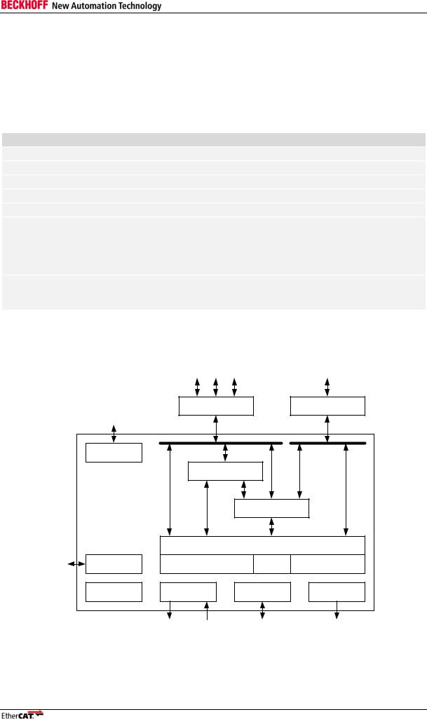
The EtherCAT IP Core is a configurable EtherCAT Slave Controller (ESC). It takes care of the EtherCAT communication as an interface between the EtherCAT fieldbus and the slave application. The EtherCAT IP Core is delivered as a configurable system so that the feature set fits the requirements perfectly and brings costs down to an optimum.
Feature
Ports
FMMUs
SyncManagers
RAM
Distributed Clocks
Process Data Interfaces
Other features
Table 1: IP Core Main Features
IP Core configurable features
1-3 MII ports or 1-3 RGMII ports 1-2 RMII ports
0-8
0-8
0-60 KB
Yes, 32 bit or 64 bit
32 Bit Digital I/O (unidirectional)
SPI Slave
8/16 bit asynchronous µController Interface
Avalon® on-chip bus
AMBA® AXI3TM on-chip bus
Example designs for easy start up included
Slave applications can run on-chip if the appropriate FPGAs with sufficient resources are used
The general functionality of the EtherCAT IP Core is shown in Figure 1:
MII ports
|
|
|
0 |
1 |
2 |
SPI / µC / Digital I/O / |
|
|
|
|
|
Avalon / AXI3 |
|||
|
|
|
|
|
|
|
|
|
|
|
AutoForwarder + |
|
PDI |
||
|
|
|
Loopback |
|
|||
|
PHY MI |
|
|
|
|||
|
|
|
|
|
|
|
|
|
|
|
|
ECAT Interface |
|
PDI Interface |
|
|
PHY |
|
|
|
|
|
|
|
Management |
|
|
|
|
|
|
|
|
|
|
FMMU |
|
|
|
|
ECAT |
|
|
|
SyncManager |
|
|
|
|
|
|
|
|
|
|
|
Processing |
|
|
|
|
|
|
|
Unit |
|
|
|
|
|
|
|
|
|
|
|
ESC address space |
|
|
Reset |
Reset |
|
Registers |
User RAM |
|
Process RAM |
|
|
Monitoring |
Distributed |
|
EEPROM |
|
Status |
|
|
Clocks |
|
|
||||
|
|
|
|
|
|
||
|
|
SYNC |
LATCH |
I²C EEPROM |
|
LEDs |
|
Figure 1: EtherCAT IP Core Block Diagram
Slave Controller – IP Core for Altera FPGAs |
III-1 |
Overview
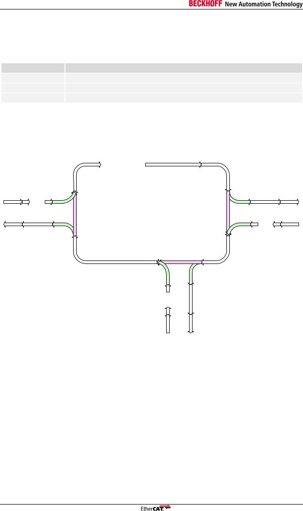
1.1Frame processing order
The frame processing order of the EtherCAT IP Core is as follows (logical port numbers are used):
Table 2: Frame Processing Order
Number of Ports Frame processing order
10→EtherCAT Processing Unit→0
20→EtherCAT Processing Unit→1 / 1→0
30→EtherCAT Processing Unit→1 / 1→2 / 2→0 (log. Ports 0,1, and 2)
Figure 2 shows the frame processing in general:
Port 0
Forwarder
Auto-
port 0 open or all ports closed |
port 0 closed |
Loopback function |
EtherCAT
Processing Unit
EtherCAT IP Core
Loopback function
port 2 closed
Loopback function |
port 1 closed |
open |
-Auto Forwarder |
port1 |
|
|
1 |
Port 1
port 2 open
Auto-
Forwarder
Port 2
Figure 2: Frame Processing
Frame Processing Example with Ports 0 and 1
A frame received at port 0 goes via the Auto-Forwarder and the Loopback function to the EtherCAT Processing Unit which processes it. Then, the frame is sent to port 1. If port 1 is open, the frame is sent out at port 1. If it is closed, the frame is forwarded by the Loopback function to port 2. Since port 2 is not configured, the Loopback function of port 2 forwards the frame to the Loopback function of port 0, and then it is sent out at port 0 – back to the master.
III-2 |
Slave Controller – IP Core for Altera FPGAs |

Overview
1.2Scope of this document
Purpose of this document is to describe the installation and configuration of the EtherCAT IP Core for Altera FPGAs. Furthermore, the signals and registers of the IP Core depending on the chosen configuration are described.
This documentation was made with the assumption that the user is familiar with the handling of the Altera Quartus® Development Environment.
1.3Scope of Delivery
The EtherCAT IP Core installation file includes:
EtherCAT IP Core (encrypted VHDL library)
Example designs
The following files which contain customer specific information are required to synthesize the IP Core. They are delivered independently of the installation file.
License File to decrypt EtherCAT IP Core: license_<company>_<Dongle/MAC ID>_<date>.dat
Encrypted Vendor ID package: pk_ECAT_VENDORID_<company>_Altera.vhd
Slave Controller – IP Core for Altera FPGAs |
III-3 |

Overview
1.4Target FPGAs
The EtherCAT IP Core for Altera® FPGAs is targeted at these FPGA families:
Altera Cyclone® II, Cyclone III, Cyclone III LS, Cyclone IV E+GX, Cyclone V
Altera Cyclone V SoC
Altera Stratix®, Stratix II, Stratix III, Stratix IV, Stratix V
Altera Arria® GX, Arria II GX, Arria II GZ, Arria V
Altera Stratix® GX, Stratix II GX
Intel® AtomTM Processor E6x5C (formerly Stellarton)
Altera MAX10
The EtherCAT IP Core is designed to support a wide range of FPGAs without modifications, because it does not instantiate dedicated FPGA resources, or rely on device specific features. Thus, the IP Core is easily portable to new FPGA families.
The complexity of the IP Core is highly configurable, so its demands for logic resources, memory blocks, and FPGA speed cover a wide range. Thus, it is not possible to run any IP Core configuration on any target FPGA with any speed grade. I.e., there are IP Core configurations requiring a faster speed grade, or a larger FPGA, or even a more powerful FPGA family.
It is necessary to run through the whole synthesis process – including timing checks –, to evaluate if the selected FPGA is suitable for a certain IP Core configuration before making the decision for the FPGA. Please consider a security margin for the logic resources to allow for minor enhancements and bug fixes of the IP Core and the user logic.
1.5Designflow requirements
For synthesis of the EtherCAT IP Core for Altera FPGAs, at least one of the following Altera Quartus II versions is needed (with latest service pack):
Altera Quartus II version 13.0
Altera Quartus II version 13.1
Altera Quartus II version 14.0
Altera Quartus II version 14.1
Higher Quartus II versions are probably supported. Installation of the latest service pack is recommended. A free version (“Web Edition”) is available from Altera (http://www.altera.com).
Optionally for using the EtherCAT IP Core with a NIOS® based Qsys design, you will need
Altera Nios II Embedded Design Suite
III-4 |
Slave Controller – IP Core for Altera FPGAs |
Overview
1.6Tested FPGA/Designflow combinations
The EtherCAT IP Core has been synthesized successfully with different Quartus II versions and FPGA families. Table 3 lists combinations of FPGA devices and design tools versions which have been synthesized or even tested in real hardware. This list does not claim to be complete, it just illustrates that the EtherCAT IP Core is designed to comply with a broad spectrum of FPGAs.
|
|
Table 3: Tested FPGA/Designflow combinations |
|
||
IP |
Family |
Device |
Designflow |
Test |
Used Example |
Core |
|
|
|
|
Designs |
|
Cyclone III |
EP3C40 |
Quartus II 13.1.4 |
Hardware |
DBC3C40 Digital |
|
|
|
|
|
I/O |
|
|
|
Cyclone III LS |
|
|
|
EP3CLS200 |
|
|
|
Quartus II 13.1.4 |
|
|
|
Synthesis |
|
|
|
|
|
|
|
|
|
|
|
|
|
|
|
|
|
|
|
|
|
|
||||
|
|
|
|
|
|
|
|
|
|
|
|
|
|
|
|
|||||
|
|
|
Cyclone IV E |
|
|
|
EP4CE55 |
|
|
|
Quartus II 14.1 |
|
|
|
Hardware |
|
|
|
DBC4CE55 Nios |
|
|
|
|
|
|
|
|
|
|
|
|
|
|
|
|
|
|||||
|
|
|
Cyclone IV E |
|
|
|
EP4CE115 |
|
|
|
Quartus II 14.1 |
|
|
|
Hardware |
|
|
|
DE2-115 Nios |
|
|
|
|
|
|
|
|
|
|
|
|
|
|
|
|
|
|
||||
|
|
|
Cyclone V |
|
|
|
5CEBA2 |
|
|
|
Quartus II 14.1 |
|
|
|
Synthesis |
|
|
|
|
|
|
|
|
|
|
|
|
|
|
|
|
|
|
|
|
|
|
||||
|
|
|
Cyclone V SoC |
|
|
|
5CSEMA5 |
|
|
|
Quartus II 14.1 |
|
|
|
Synthesis |
|
|
|
|
|
|
|
|
|
|
|
|
|
|
|
|
|
|
|
|
|
|
||||
|
|
|
Stratix III |
|
|
|
EP3SE50 |
|
|
|
Quartus II 13.1.4 |
|
|
|
Synthesis |
|
|
|
|
|
|
|
|
|
|
|
|
|
|
|
|
|
|
|
|
|
|
||||
|
|
|
Stratix IV E |
|
|
|
EP4SE230 |
|
|
|
Quartus II 14.1 |
|
|
|
Synthesis |
|
|
|
|
|
3.0.10 |
|
|
|
|
||||||||||||||||
|
|
|
|
|
|
|
|
|
|
|
|
|
|
|
|
|
|
|
|
|
|
|
Stratix IV GT |
|
|
|
EP4S40G |
|
|
|
Quartus II 14.1 |
|
|
|
Synthesis |
|
|
|
|
|
|
|
|
|
|
|
|
|
|
|
|
|
|
|
|
|
|
|
||||
|
|
|
|
|
|
|
|
|
|
|
|
|
|
|
|
|
||||
|
|
|
Stratix IV GX |
|
|
|
EP4SGX70 |
|
|
|
Quartus II 14.1 |
|
|
|
Synthesis |
|
|
|
|
|
|
|
|
|
|
|
|
|
|
|
|
|
|
|
|
|
|
||||
|
|
|
Stratix V |
|
|
|
5SGSMD4 |
|
|
|
Quartus II 14.1 |
|
|
|
Synthesis |
|
|
|
|
|
|
|
|
|
|
|
|
|
|
|
|
|
|
|
|
|
|
||||
|
|
|
Arria II GX |
|
|
|
EP2AGX45 |
|
|
|
Quartus II 14.1 |
|
|
|
Synthesis |
|
|
|
|
|
|
|
|
|
|
|
|
|
|
|
|
|
|
|
|
|
|
||||
|
|
|
Arria V |
|
|
|
5AGXMB3 |
|
|
|
Quartus II 14.1 |
|
|
|
Synthesis |
|
|
|
|
|
|
|
|
|
|
|
|
|
|
|
|
|
|
|
|
|
|
||||
|
|
|
Arria V GZ |
|
|
|
5AGZME5 |
|
|
|
Quartus II 14.1 |
|
|
|
Synthesis |
|
|
|
|
|
|
|
|
|
|
|
|
|
|
|
|
|
|
|
|
|
|
||||
|
|
|
Intel Atom |
|
|
|
EP2AGXE |
|
|
|
Quartus II 13.1.4 |
|
|
|
Synthesis |
|
|
|
|
|
|
|
|
E6x5C |
|
|
|
6XXFPGA |
|
|
|
|
|
|
|
|
|
|
|
|
|
|
|
|
|
|
|
|
|
|
|
|
|
|
|
|
|
|
||||
|
|
|
MAX10 |
|
|
|
10M40DA |
|
|
|
Quartus II 14.1 |
|
|
|
Synthesis |
|
|
|
|
|
|
|
|
|
|
|
|
|
|
|
|
|
|
|
|
|
|
|
|
|
|
NOTE: Synthesis test means analysis, synthesis, fitter, and assembler. Hardware test means the design was operational using real hardware.
NOTE: Turn on Analysis & Synthesis option: Auto RAM Replacement, otherwise the RAM inside the IP Core will be implemented with individual registers.
Refer to the Hardware Data Sheet Section III Addendum available at the Beckhoff homepage (http://www.beckhoff.com) for latest updates regarding device support, design flow compatibility, and known issues.
Slave Controller – IP Core for Altera FPGAs |
III-5 |
Overview
1.7Release Notes
EtherCAT IP Core updates deliver feature enhancements and removed restrictions. Feature enhancements are not mandatory regarding conformance to the EtherCAT standard. Restrictions have to be judged whether they are relevant in the user’s configuration or not, or if workarounds are possible.
Table 4: Release notes
|
Version |
|
|
|
Release notes |
|
|
|
|
|
|
||
|
|
|
|
|
|
|
3.0.0Update to Quartus II 11.0 with Qsys support
(3/2013) |
|
|
Removed small/medium/large register sets, added updated preset configurations |
|
|
Enhancements: |
|
|
|
|
Increased PDI performance |
|
|
Support for 8/16/32/64 bit Avalon and AXI3TM interface |
|
|
|
Support for RGMII ports (added DE2-115 RGMII example design) |
|
|
|
|
|
|
|
Native support for FX PHYs |
|
|
|
Support for individual PHY address configuration and reading out this |
|
|
|
|
configuration |
|
|
Support for static or dynamic PHY address configuration |
|
|
|
Support for 0 KB Process RAM, DC Sync/Latch signals individually configurable, |
|
|
|
|
LED test added |
|
|
Support for PDI SyncManager/IRQ acknowledge by Write command |
|
|
|
Device emulation is now configured in the GUI statically. |
|
|
|
Restrictions of this version, which are removed in V3.0.1: |
|
|
|
Distributed Clocks are not available |
|
|
|
AXI PDI is not available |
|
|
|
RMII is not available |
|
|
|
A time limit of 1 hour for evaluation purposes is enabled even without OpenCore |
|
|
|
|
Plus |
|
|
The DBC3C40 and DBC4CE55 example designs are occasionally causing the |
|
|
|
|
PHY port 0 to fall into Isolate mode |
|
|
Restrictions of this version, which are removed in V3.0.2: |
|
EEPROM Emulation is not available
General purpose output byte 7 is not available Restrictions of this version, which are removed in V3.0.5:
The AXI PDI may occasionally write incorrect data if simultaneous read and write accesses occur repeatedly.
RX FIFO size is not initialized by SII EEPROM
Restrictions of this version, which are removed in V3.0.6:
The ERR LED does not allow overriding using the ERR LED Override register 0x0139 while AL Status register Error Indication bit 0x0130[4] is set.
Restrictions of this version, which are removed in V3.0.9:
The AXI PDI may not complete an access occasionally if overlapping read and write accesses occur, causing the processor to wait endlessly.
The AXI PDI does not execute read accesses correctly if ARSIZE is smaller than the AXI bus width.
Restrictions of this version, which are removed in V3.0.10:
The last 4 Kbyte Process Data RAM (0xF000:0xFFFF) cannot be used in the 60 Kbyte RAM configuration.
The AXI PDI may write to wrong bytes if the write data is valid before the address,
III-6 |
Slave Controller – IP Core for Altera FPGAs |
Overview
|
Version |
|
|
|
Release notes |
|
|
|
|
|
|
||
|
|
|
|
|
|
|
which is typically true for AXI4LITE.
The AXI PDI may read additional bytes after the intended bytes.
The AXI PDI may write additional bytes to byte lanes without byte enable, if User RAM (0x0F80:0x0FFF) or Process Data RAM (0x01000 ff.) is written, if the actual write address on the bus is 32 bit aligned (AWADDR[1:0]=00), and if one or more of the lower byte enables/byte strobes (WSTRB) is not set.
3.0.1Enhancements:
|
|
|
Integration into Quartus II 13.0 added |
(3/2013) |
|||
|
|
Removed PDI_AXI_IRQ_DC_SYNC0/1 signals to support Quartus II 12.1/13.0 |
|
|
|
|
(use Qsys IRQ bridge to use DC SyncSignals as interrupts) |
|
|
Restrictions of previous versions which are removed in this version: |
|
|
|
Distributed Clocks are available |
|
|
|
AXI PDI is available |
|
|
|
|
RMII is available |
|
|
|
|
|
|
A time limit of 1 hour for evaluation purposes is only enabled with OpenCore Plus |
|
|
|
The DBC3C40 and DBC4CE55 example designs are preventing the PHY port 0 |
|
|
|
|
from falling into Isolate mode |
|
|
Restrictions of this version, which are removed in V3.0.2: |
|
EEPROM Emulation is not available
General purpose output byte 7 is not available Restrictions of this version, which are removed in V3.0.5:
The AXI PDI may occasionally write incorrect data if simultaneous read and write accesses occur repeatedly.
RX FIFO size is not initialized by SII EEPROM
Restrictions of this version, which are removed in V3.0.6:
The ERR LED does not allow overriding using the ERR LED Override register 0x0139 while AL Status register Error Indication bit 0x0130[4] is set.
Restrictions of this version, which are removed in V3.0.9:
The AXI PDI may not complete an access occasionally if overlapping read and write accesses occur, causing the processor to wait endlessly.
The AXI PDI does not execute read accesses correctly if ARSIZE is smaller than the AXI bus width.
Restrictions of this version, which are removed in V3.0.10:
The last 4 Kbyte Process Data RAM (0xF000:0xFFFF) cannot be used in the 60 Kbyte RAM configuration.
The AXI PDI may write to wrong bytes if the write data is valid before the address, which is typically true for AXI4LITE.
The AXI PDI may read additional bytes after the intended bytes.
The AXI PDI may write additional bytes to byte lanes without byte enable, if User RAM (0x0F80:0x0FFF) or Process Data RAM (0x01000 ff.) is written, if the actual write address on the bus is 32 bit aligned (AWADDR[1:0]=00), and if one or more of the lower byte enables/byte strobes (WSTRB) is not set.
Slave Controller – IP Core for Altera FPGAs |
III-7 |
Overview
|
Version |
|
|
|
Release notes |
|
|
|
|
|
|
||
|
|
|
|
|
|
|
3.0.2Enhancements:
(5/2013) |
|
MI link detection: relaxed checking of PHY register 9 (1000Base-T Master-Slave |
|
|
Control register) |
|
|
Restrictions of previous versions which are removed in this version: |
EEPROM Emulation is available
General purpose output byte 7 is available Restrictions of this version, which are removed in V3.0.5:
The AXI PDI may occasionally write incorrect data if simultaneous read and write accesses occur repeatedly.
RX FIFO size is not initialized by SII EEPROM
Restrictions of this version, which are removed in V3.0.6:
The ERR LED does not allow overriding using the ERR LED Override register 0x0139 while AL Status register Error Indication bit 0x0130[4] is set.
Restrictions of this version, which are removed in V3.0.9:
The AXI PDI may not complete an access occasionally if overlapping read and write accesses occur, causing the processor to wait endlessly.
The AXI PDI does not execute read accesses correctly if ARSIZE is smaller than the AXI bus width.
Restrictions of this version, which are removed in V3.0.10:
The last 4 Kbyte Process Data RAM (0xF000:0xFFFF) cannot be used in the 60 Kbyte RAM configuration.
The AXI PDI may write to wrong bytes if the write data is valid before the address, which is typically true for AXI4LITE.
The AXI PDI may read additional bytes after the intended bytes.
The AXI PDI may write additional bytes to byte lanes without byte enable, if User RAM (0x0F80:0x0FFF) or Process Data RAM (0x01000 ff.) is written, if the actual write address on the bus is 32 bit aligned (AWADDR[1:0]=00), and if one or more of the lower byte enables/byte strobes (WSTRB) is not set.
III-8 |
Slave Controller – IP Core for Altera FPGAs |
Overview
|
Version |
|
|
|
Release notes |
|
|
|
|
|
|
||
|
|
|
|
|
|
|
3.0.5Enhancements:
(2/2014) |
|
Improved MegaWizard GUI: shows on-chip bus speed and configuration details |
|
|
Example designs using Qsys include .qip file instead of .qsys file (Qsys |
|
|
constraints are used now) |
|
|
Restrictions of previous versions which are removed in this version: |
|
|
The AXI PDI writes correct data if simultaneous read and write accesses occur |
|
|
repeatedly. |
|
|
RX FIFO size is properly initialized by SII EEPROM |
|
|
Restrictions of this version, which are removed in V3.0.6: |
|
|
The ERR LED does not allow overriding using the ERR LED Override register |
|
|
0x0139 while AL Status register Error Indication bit 0x0130[4] is set. |
|
|
Restrictions of this version, which are removed in V3.0.9: |
|
|
|
|
|
The AXI PDI may not complete an access occasionally if overlapping read and |
|
|
write accesses occur, causing the processor to wait endlessly. |
|
|
The AXI PDI does not execute read accesses correctly if ARSIZE is smaller than |
|
|
the AXI bus width. |
|
|
Restrictions of this version, which are removed in V3.0.10: |
|
|
The last 4 Kbyte Process Data RAM (0xF000:0xFFFF) cannot be used in the 60 |
|
|
Kbyte RAM configuration. |
|
|
The AXI PDI may write to wrong bytes if the write data is valid before the address, |
|
|
which is typically true for AXI4LITE. |
|
|
The AXI PDI may read additional bytes after the intended bytes. |
|
|
The AXI PDI may write additional bytes to byte lanes without byte enable, if User |
|
|
RAM (0x0F80:0x0FFF) or Process Data RAM (0x01000 ff.) is written, if the actual |
|
|
write address on the bus is 32 bit aligned (AWADDR[1:0]=00), and if one or more |
|
|
of the lower byte enables/byte strobes (WSTRB) is not set. |
Slave Controller – IP Core for Altera FPGAs |
III-9 |
Overview
|
Version |
|
|
|
Release notes |
|
|
|
|
|
|
||
|
|
|
|
|
|
|
3.0.6Enhancements:
(4/2014) |
|
The Sync/Latch PDI Configuration register 0x0151 shows the same value as |
|
|
previous IP Core versions. The actual configuration is not affected, since it is fixed |
|
|
by the IP Core configuration. |
|
|
Avalon/AXI timing: Quartus might infer an additional clock control buffer into the |
|
|
on-chip-bus clock signal, causing higher jitter/delay. This clock buffer is now |
|
|
avoided, leading to better timing results. |
|
|
Added support for unaligned AXI burst transfers. |
|
|
Restrictions of previous versions which are removed in this version: |
|
|
The ERR LED allows overriding using the ERR LED Override register 0x0139 |
|
|
while AL Status register Error Indication bit 0x0130[4] is set. The override flag is |
|
|
now cleared upon a rising edge of 0x0130[4], and it can be set again afterwards. |
|
|
Restrictions of this version, which are removed in V3.0.9: |
|
|
|
|
|
The AXI PDI may not complete an access occasionally if overlapping read and |
|
|
write accesses occur, causing the processor to wait endlessly. |
|
|
The AXI PDI does not execute read accesses correctly if ARSIZE is smaller than |
|
|
the AXI bus width. |
|
|
Restrictions of this version, which are removed in V3.0.10: |
The last 4 Kbyte Process Data RAM (0xF000:0xFFFF) cannot be used in the 60 Kbyte RAM configuration.
The AXI PDI may write to wrong bytes if the write data is valid before the address, which is typically true for AXI4LITE.
The AXI PDI may read additional bytes after the intended bytes.
The AXI PDI may write additional bytes to byte lanes without byte enable, if User RAM (0x0F80:0x0FFF) or Process Data RAM (0x01000 ff.) is written, if the actual write address on the bus is 32 bit aligned (AWADDR[1:0]=00), and if one or more of the lower byte enables/byte strobes (WSTRB) is not set.
3.0.9Enhancements:
(9/2014) |
|
The Altera DE2-115 example designs have been updated to support Quartus 14.0 |
|
|
(connected PLL areset signal) |
|
|
The PDI watchdog status 0x0110[1] now shows value ‘1’ (watchdog reloaded) if |
|
|
the PDI watchdog is configured to be not available. |
|
|
The ESI XML device description does not use special data types anymore. |
|
|
Restrictions of previous versions which are removed in this version: |
|
|
The AXI PDI completes accesses if overlapping read and write accesses occur. |
|
|
The AXI PDI executes read accesses correctly if ARSIZE is smaller than the AXI |
|
|
bus width. |
|
|
Restrictions of this version, which are removed in V3.0.10: |
|
|
The last 4 Kbyte Process Data RAM (0xF000:0xFFFF) cannot be used in the 60 |
|
|
Kbyte RAM configuration. |
|
|
The AXI PDI may write to wrong bytes if the write data is valid before the address, |
|
|
which is typically true for AXI4LITE. |
|
|
The AXI PDI may read additional bytes after the intended bytes. |
|
|
The AXI PDI may write additional bytes to byte lanes without byte enable, if User |
|
|
RAM (0x0F80:0x0FFF) or Process Data RAM (0x01000 ff.) is written, if the actual |
|
|
write address on the bus is 32 bit aligned (AWADDR[1:0]=00), and if one or more |
|
|
of the lower byte enables/byte strobes (WSTRB) is not set. |
III-10 |
Slave Controller – IP Core for Altera FPGAs |
Overview
Version
3.0.10
(1/2015)
Release notes
The EL9800/FB1122 example designs have been removed because these evaluation boards are no longer available.
Enhancements:
For EEPROM Emulation, the CRC error bit 0x0502[11] can be written via PDI to indicate CRC errors during a reload command.
Restrictions of previous versions which are removed in this version:
The last 4 Kbyte Process Data RAM (0xF000:0xFFFF) can be used in the 60 Kbyte RAM configuration.
The AXI PDI does not write to wrong bytes if the write data is valid before the address.
The AXI PDI does not read additional bytes after the intended bytes.
The AXI PDI does not write to byte lanes without byte enable.
Slave Controller – IP Core for Altera FPGAs |
III-11 |
Overview
1.7.1Major differences between V2.4.x and V3.0.x
The EtherCAT IP Core V3.0.x versions have these advantages compared with the V2.4.x versions:
Increased PDI performance (average latency internally at least by a factor of 2 faster; worst case latency even better)
Support for 8/16/32/64 bit Avalon and AXI3TM interface
Support for RGMII ports
Native support for FX PHYs
Flexible PHY address configuration
Support for PDI SyncManager/IRQ acknowledge by Write command (required for wide on-chip- busses)
More detailed configuration
The higher PDI performance increases the resource requirements of the V3.0.x versions compared with the V2.4.x versions. New development is focused on the V3.0.x versions.
1.7.2Reading IP Core version from device
The IP Core version, denoted as X.Y.Z (e.g., 2.4.0), consists of three values X, Y, and Z. These values can be read out in registers 0x0001 and 0x0002.
|
|
Table 5: Register Revision (0x0001) |
|
|
||
|
|
|
|
|
|
|
Bit |
|
Description |
|
ECAT |
|
PDI |
|
|
|
|
|
|
|
7:0 |
|
IP Core major version X |
|
r/- |
|
r/- |
|
|
|
|
|
|
|
|
|
Table 6: Register Build (0x0002:0x0003) |
||
Bit |
Description |
|
ECAT |
PDI |
3:0 |
IP Core maintenance version Z |
r/- |
r/- |
|
7:4 |
IP Core minor version Y |
r/- |
r/- |
|
15:8 |
Patch level: |
|
r/- |
r/- |
|
0x00: |
original release |
|
|
|
0x01-0x0F: |
patch level of original release |
|
|
Reset Value
IP Core dep.
Reset Value
IP Core dep.
IP Core dep.
IP Core dep.
III-12 |
Slave Controller – IP Core for Altera FPGAs |

Overview
1.8Design flow
The design flow for creating an EtherCAT Slave Controller based on the EtherCAT IP Core is shown in the following picture:
Production |
Development |
|
Vendor ID |
Evaluation |
|
|
|
package |
|
VHDL |
Application |
|
|
|
specific ESC |
encrypted |
Vendor |
|
|
Verilog |
|
|||
|
VHDL |
ID |
|
|
Schematic |
sources |
|
||
|
|
|
||
User logic |
|
IP Core |
|
|
|
|
installation |
|
|
|
Synthesis |
or |
|
|
|
MAC ID |
MAC ID |
||
|
|
|||
|
|
Dongle |
Dongle |
|
|
|
License file (full) |
License file (eval) |
|
|
bit- |
|
|
bit- |
|
stream |
|
|
stream |
|
|
|
|
(OpenCore Plus) |
|
FPGA configuration file |
|
|
FPGA configuration file |
Download |
Download |
|
|
Download |
utility |
utility |
|
|
utility |
Buy-out license / |
|
|
|
|
Quantity-based license |
|
|
|
JTAG |
(license agreement) |
|
|
|
|
|
|
|
tethered |
|
grants permission |
|
|
|
(else timebomb) |
FPGA |
FPGA |
|
|
FPGA |
FPGA |
|
|
|
|
FPGA |
|
|
|
(OpenCore Plus) |
Customer
Figure 3: Design flow
Slave Controller – IP Core for Altera FPGAs |
III-13 |

Overview
1.9OpenCore Plus Evaluation
The EtherCAT IP Core for Altera FPGAs supports OpenCore Plus evaluation. A special License File with OpenCore Plus support is issued for each user, together with the IP Core Vendor ID package. For further information on OpenCore Plus, refer to the Altera Application Note 320 “OpenCore Plus Evaluation of Megafunctions”, available from Altera (http://www.altera.com).
A design with an OpenCore Plus EtherCAT IP Core is subject to some restrictions:
Only a time limited programming file (<design_name>_time_limited.sof) for the Altera Quartus II Programmer is generated. Other programming files (e.g., .rbf, .pof) are not generated.
For hardware testing, the ESC design has to be connected to the PC running the Altera Quartus II Programmer using a programming adapter with a JTAG connection. The EtherCAT IP Core is fully functional while the adapter is connected.
If the connection is interrupted, the EtherCAT IP Core will discontinue its function after approximately 1 hour.
The OpenCore Plus version slightly increases the resource consumption of the IP Core.
The OpenCore Plus programming file must not be distributed/sold.
A vendor ID package is required for both evaluation and full license. It is recommended to use an evaluation vendor ID (package) for evaluation, and the original vendor ID for production. The evaluation vendor ID is beginning with “0xE.......” and ends with the original vendor ID digits.
Evaluation vendor IDs cannot pass the EtherCAT conformance tests.
OpenCore Plus Issues
Sometimes additional top-level pins appear in the OpenCore Plus design, these signals should be grounded externally if possible. This is a Quartus OpenCore Plus integration issue, not an EtherCAT IP Core issue. The signals will not appear if a full license is used. Additionally, do not use incremental synthesis together with OpenCore Plus, since this was found to produce defective designs similar to the OpenCore Plus integration issue.
Sometimes timing requirements are not met with OpenCore Plus. Experience shows that timing violations related to the clock altera_reserved_tck can be ignored.
Upgrading to a Full License
A design using an OpenCore Plus EtherCAT IP Core does not have to be changed when upgrading to a full license, only the full License File has to be installed instead of the OpenCore Plus License File. A re-generation of the EtherCAT IP Core (running through the MegaWizard) and a new synthesis run is necessary to generate the unlimited programming files.
III-14 |
Slave Controller – IP Core for Altera FPGAs |

Overview
1.10 Simulation
A behavioral simulation model of the EtherCAT IP core is not available because of its size and complexity. Thus, simulation of the entire EtherCAT IP Core is not supported, and the EDA Netlist Writer cannot be used for designs which contain the EtherCAT IP Core. In most cases, simulation of the EtherCAT IP Core is not necessary, as the IP Core was thoroughly tested and the interfaces are standardized (Ethernet, Avalon) or simple and well described. Problems at the interface level can often be solved with a scope shot of the interface signals.
Nevertheless, customer designs using the Avalon or AXI on-chip bus can easily be simulated using a Bus Functional Model of the on-chip bus slave interface instead of a simulation model of the entire EtherCAT IP Core.
From the processor’s view, the EtherCAT IP Core is a memory (or a bunch of registers). For processor bus verification, the EtherCAT IP Core can be substituted by another IP core with Avalon/AXI slave interface which behaves like a memory as well. The EtherCAT IP Core can be replaced for simulation by e.g.:
Altera On-Chip Memory slave
Avalon/AXI slave created with the Qsys
Slave Controller – IP Core for Altera FPGAs |
III-15 |
Features and Registers
2 Features and Registers
2.1Features
Table 7: IP Core Feature Details
|
|
|
|
|
IP Core |
|
|
|
|
|
|
|
|
|
Feature |
|
|
|
Altera® |
|
|
|
|
|
|
V3.0.10 |
|
|
|
|
|
|
|
|
|
|
|
||||
|
EtherCAT Ports |
|
|
|
1-3 |
|
|
|
|
|
|||
|
Permanent ports |
|
|
|
1-3 |
|
|
|
|
|
|
|
|
|
Optional Bridge port 3 (EBUS or |
|
|
|
- |
|
|
MII) |
|
|
|
|
|
|
|
|
|
|
|
|
|
|
|
|
|||
|
EBUS ports |
|
|
|
- |
|
|
|
|
|
|||
|
MII ports |
|
|
|
0-3 |
|
|
|
|
|
|||
|
RMII ports |
|
|
|
0-2 |
|
|
|
|
|
|||
|
RGMII ports |
|
|
|
0-3 |
|
|
|
|
|
|
||
|
Port 0 |
|
|
|
x |
|
|
|
|
|
|
||
|
Ports 0, 1 |
|
|
|
x |
|
|
|
|
|
|
||
|
Ports 0, 1, 2 |
|
|
|
x |
|
|
|
|
|
|||
|
Ports 0, 1, 3 |
|
|
|
- |
|
|
|
|
|
|||
|
Ports 0, 1, 2, 3 |
|
|
|
- |
|
|
|
|
|
|||
|
EtherCAT mode |
|
|
|
Direct |
|
|
|
|
|
|||
|
Slave Category |
|
|
|
Full Slave |
|
|
|
|
|
|
||
|
Position addressing |
|
|
|
x |
|
|
|
|
|
|
||
|
Node addressing |
|
|
|
x |
|
|
|
|
|
|
||
|
Logical addressing |
|
|
|
x |
|
|
|
|
|
|
||
|
Broadcast addressing |
|
|
|
x |
|
|
|
|
|
|
|
|
Physical Layer General Features
FIFO Size configurable |
x |
|
(0x0100[18:16]) |
||
|
||
FIFO Size default from SII |
x |
|
EEPROM |
||
|
||
Auto-Forwarder checks CRC and |
x |
|
SOF |
||
|
||
Forwarded RX Error indication, |
|
|
detection and Counter |
x |
|
(0x0308:0x030B) |
|
|
Lost Link Counter |
c |
|
(0x0310:0x0313) |
||
|
||
Prevention of circulating frames |
x |
|
Fallback: Port 0 opens if all ports |
x |
|
are closed |
||
|
||
VLAN Tag and IP/UDP support |
x |
|
Enhanced Link Detection per port |
x |
|
configurable |
||
|
||
General Ethernet Features |
|
|
(MII/RMII/RGMII) |
|
|
MII Management Interface |
c |
|
(0x0510:0x051F) |
||
|
||
Supported PHY Address Offsets |
any |
|
Individual port PHY addresses |
x |
|
Port PHY addresses readable |
x |
|
Link Polarity configurable |
User logic |
|
Enhanced Link Detection |
x |
|
supported |
||
|
||
FX PHY support (native) |
x |
|
PHY reset out signals |
x |
|
Link detection using PHY signal |
x |
|
(LED) |
||
|
||
MI link status and configuration |
c |
|
MI controllable by PDI |
x |
|
(0x0516:0x0517) |
||
|
||
MI read error (0x0510.13) |
x |
|
MI PHY configuration update |
x |
|
status (0x0518.5) |
||
|
||
MI preamble suppression |
x |
|
Additional MCLK |
x |
|
Gigabit PHY configuration |
x |
|
Gigabit PHY register 9 relaxed |
x |
|
check |
||
|
||
FX PHY configuration |
x |
|
Transparent Mode |
- |
IP Core |
|
IP Core |
IP Core |
|||
Altera |
® |
|
Altera |
® |
||
|
Feature |
Altera® |
|
|||
V3.0.0- |
|
V3.0.10 |
V3.0.0- |
|||
3.0.9 |
|
|
3.0.9 |
|
||
|
|
|
|
|||
1-3 |
|
MII Features |
|
|
|
|
1-3 |
|
CLK25OUT as PHY clock source |
User logic |
User logic |
||
- |
|
Bootstrap TX Shift settings |
c |
c |
|
|
|
|
|
|
|
||
|
|
Automatic TX Shift setting (with |
c |
c |
|
|
- |
|
TX_CLK) |
|
|||
|
|
|
|
|||
0-3 |
|
TX Shift not necessary (PHY |
- |
- |
|
|
|
|
TX_CLK as clock source) |
|
|||
0-2 |
|
|
|
|
||
|
|
|
|
|
||
0-3 |
|
FIFO size reduction steps |
2 |
2 |
|
|
|
|
|
|
|
||
x |
|
PDI General Features |
|
|
|
|
|
|
|
|
|
||
x |
|
Increased PDI performance |
x |
x |
|
|
|
|
|
|
|
||
x |
|
Extended PDI Configuration |
x |
x |
|
|
|
(0x0152:0x0153) |
|
||||
|
|
|
|
|
||
- |
|
PDI Error Counter (0x030D) |
c |
c |
|
|
|
|
|
||||
- |
|
PDI Error Code (0x030E) |
c |
c |
|
|
|
|
|
||||
Direct |
CPU_CLK output (10, 20, 25 |
|
|
|
||
|
|
User logic |
User logic |
|||
Full Slave |
MHz) |
|||||
|
|
|
||||
x |
|
SOF, EOF, WD_TRIG and |
x |
x |
|
|
|
|
WD_STATE independent of PDI |
|
|||
x |
|
|
|
|
||
|
|
|
|
|
||
x |
|
Available PDIs and PDI features |
- |
- |
|
|
|
depending on port configuration |
|
||||
|
|
|
|
|
||
x |
|
PDI selection at run-time (SII |
|
|
|
|
|
|
- |
- |
|
||
|
|
EEPROM) |
|
|||
|
|
|
|
|
||
x |
|
PDI active immediately (SII |
x |
x |
|
|
|
EEPROM settings ignored) |
|
||||
|
|
|
|
|
||
x |
|
PDI function acknowledge by |
c |
c |
|
|
|
write |
|
||||
|
|
|
|
|
||
x |
|
PDI Information register |
c |
c |
|
|
|
0x014E:0x014F |
|
||||
|
|
|
|
|
||
|
|
Digital I/O PDI |
x |
x |
|
|
x |
|
Digital I/O width [bits] |
8/16/24/32 |
8/16/24/32 |
||
|
|
|||||
|
|
PDI Control register value |
4 |
4 |
|
|
c |
|
(0x0140:0x0141) |
|
|||
|
|
|
|
|||
x |
|
Control/Status signals: |
7 |
7 |
|
|
|
|
|
|
|
||
|
|
LATCH_IN |
x |
x |
|
|
x |
|
SOF |
x |
x |
|
|
|
|
|
||||
x |
|
OUTVALID |
x |
x |
|
|
x |
|
WD_TRIG |
x |
x |
|
|
|
|
|
|
|
||
|
|
OE_CONF |
- |
- |
|
|
|
|
OE_EXT |
x |
x |
|
|
|
|
EEPROM_ |
x |
x |
|
|
c |
|
Loaded |
|
|||
|
|
|
|
|||
|
|
|
|
|
WD_STATE |
|
|
|
|
x |
|
|
|
x |
|
|
any |
|
|||||||||||||
|
|
|
|
|
|
|
|
|
|
|
|
|
|
|
|
|
|
|
|
|
EOF |
|
|
|
|
x |
|
|
|
x |
|
|
x |
|
|||||||||||||
|
|
|
|
|
|
|
|
|
|
|
|
|
|
|
|
|
x |
|
|
|
Granularity of direction |
|
|
|
|
8 |
|
|
|
8 |
|
|
|
|
|
configuration [bits] |
|
|
|
|
|
|
|
||||
|
|
|
|
|
|
|
|
|
|
|
|
|
|
|
|
|
User logic |
|
|
|
Bidirectional mode |
|
|
|
|
- (User |
|
|
|
- (User |
|
|
|
|
|
|
|
|
|
|
|
|
|
|
|||
|
x |
|
|
|
|
|
|
|
|
logic) |
|
|
|
logic) |
|
|
|
|
|
|
|
|
|
|
|
|
|
|
|
|
|
|
|
|
|
|
Output high-Z if WD expired |
|
|
|
|
User logic |
|
|
|
User logic |
|
|
|
|
|
|
|
|
|
|
|
|
|
|
|
|
|
|
x |
|
|
|
|
|
|
|
|
|
|
|
|
|
|
|
|
|
|
Output 0 if WD expired |
|
|
|
|
x |
|
|
|
x |
|
|
|
|
|
|
|
|
|
|
|
|
|
|
|
|||
|
x |
|
|
|
Output with EOF |
|
|
|
|
x |
|
|
|
x |
|
|
|
|
|
|
|
|
|
|
|
|
|
|
|||
|
x |
|
|
|
Output with DC SyncSignals |
|
|
|
|
x |
|
|
|
x |
|
|
|
|
|
|
|
|
|
|
|
|
|
|
|
|
|
|
|
|
|
|
Input with SOF |
|
|
|
|
x |
|
|
|
x |
|
|
c |
|
|||||||||||||
|
|
|
|
|
|
|
|
|
|
|
|
|
|
|
|
|
|
|
|
|
Input with DC SyncSignals |
|
|
|
|
x |
|
|
|
x |
|
|
x |
|
|
|
SPI Slave PDI |
|
|
|
|
x |
|
|
|
x |
|
|
|
|
|
|
|
|
|
|
|
|
|
|
|||
|
|
|
|
|
|
|
|
|
|
|
|
|
|
|
|
|
x |
|
|
|
Max. SPI clock [MHz] |
|
|
|
30 |
|
|
|
30 |
|
|
|
|
|
|
|
|
|
|
|
|
|
|
|
|
|
|
|
x |
|
|
|
SPI modes configurable |
|
|
|
|
x |
|
|
|
x |
|
|
|
|
|
(0x0150[1:0]) |
|
|
|
|
|
|
|
|
|||
|
|
|
|
|
|
|
|
|
|
|
|
|
|
|
|
|
|
|
|
|
|
|
|
|
|
|
|
|
|
|
|
|
x |
|
|
|
SPI_IRQ driver configurable |
|
|
|
|
x |
|
|
|
x |
|
|
|
|
|
|
(0x0150[3:2]) |
|
|
|
|
|
|
|
|
||
|
x |
|
|
|
|
|
|
|
|
|
|
|
|
|
|
|
|
|
|
|
|
|
|
|
|
|
|
|
|
|
|
|
x |
|
|
|
SPI_SEL polarity configurable |
|
|
|
|
x |
|
|
|
x |
|
|
|
|
|
(0x0150.4) |
|
|
|
|
|
|
|
|
|||
|
|
|
|
|
|
|
|
|
|
|
|
|
|
|
|
|
x |
|
|
|
Data out sample mode |
|
|
|
|
x |
|
|
|
x |
|
|
|
|
|
|
configurable (0x0150.5) |
|
|
|
|
|
|
|
|
||
|
|
|
|
|
|
|
|
|
|
|
|
|
|
|
|
|
x |
|
|
|
Busy signaling |
- |
|
- |
|
||||||
|
|
|
|
|
|
|
|||||||||
-
III-16 |
Slave Controller – IP Core for Altera FPGAs |
Features and Registers
Feature
Wait State byte(s)
Number of address extension byte(s)
2/4 Byte SPI master support
Extended error detection (read busy violation)
SPI_IRQ delay
Status indication
EEPROM_
Loaded signal
Asynchronous µController PDI
Extended µC configuration bits 0x0150[7:4], 0x0152:0x0153
ADR[15:13] available (000b if not
available)
EEPROM_Loaded signal
RD polarity configurable (0x0150.7)
Read BUSY delay (0x0152.0)
Write after first edge (0x0152.2)
Synchronous µController PDI
On-Chip Bus PDI
Avalon®
OPB®
PLB v4.6®
AXI3TM
AXI4TM
AXI4 LITETM
Bus clock [MHz] (N=1,2,3,…)
Data bus width [bits]
Prefetch cycles
DC SyncSignals available directly and as IRQ
Bus clock multiplier in register 0x0150[6:0]
EEPROM_
Loaded signal
EtherCAT Bridge (port 3, EBUS/MII)
General Purpose I/O
GPO bits
GPI bits
GPIO available independent of
PDI or port configuration
GPIO available without PDI
Concurrent access to GPO by
ECAT and PDI
ESC Information
Basic Information (0x0000:0x0006)
Port Descriptor (0x0007)
ESC Features supported (0x0008:0x0009)
Extended ESC Feature Availability in User RAM (0x0F80 ff.)
Write Protection (0x0020:0x0031)
Data Link Layer Features
ECAT Reset (0x0040)
PDI Reset (0x0041)
ESC DL Control (0x0100:0x0103) bytes
EtherCAT only mode (0x0100.0)
Temporary loop control (0x0100.1)
FIFO Size configurable (0x0100[18:16])
Configured Station Address (0x0010:0x0011)
Configured Station Alias (0x0100.24, 0x0012:0x0013)
IP Core |
IP Core |
|
IP Core |
IP Core |
||
Altera |
® |
|
Altera |
® |
||
Altera® |
|
Feature |
Altera® |
|
||
V3.0.10 |
V3.0.0- |
|
V3.0.10 |
V3.0.0- |
||
3.0.9 |
|
|
3.0.9 |
|
||
|
|
|
|
|
||
x |
x |
Physical Read/Write Offset |
c |
c |
|
|
(0x0108:0x0109) |
||
|
|
|
|
|
any |
any |
Application Layer Features |
|
|
|
|
|
|
x |
x |
Extended AL Control/Status bits |
x |
x |
|
|
(0x0120[15:5], 0x0130[15:5]) |
||
|
|
|
|
|
x |
x |
AL Status Emulation (0x0140.8) |
x |
x |
|
|
|||
x |
x |
AL Status Code (0x0134:0x0135) |
c |
c |
x |
x |
Interrupts |
|
|
|
x |
|
|
|
x |
|
|
|
ECAT Event Mask |
|
|
|
|
|
|
|
|
(0x0200:0x0201) |
|
||
|
|
|
|
|
|
|
|
|
|
|
|
|
|
|
|
|
|
|
|
||
|
8/16 bit |
|
|
|
8/16 bit |
|
|
|
AL Event Mask (0x0204:0x0207) |
|
|
|
|
|
|
|
|
|
|
|
|
|
x |
|
|
|
x |
|
|
|
ECAT Event Request |
|
|
|
|
|
|
|
|
(0x0210:0x0211) |
|
||
|
|
|
|
|
|
|
|
|
|
|
|
|
|
|
|
|
|
|
|
|
|
|
x |
|
|
|
x |
|
|
|
AL Event Request |
|
|
|
|
|
|
|
|
(0x0220:0x0223) |
|
||
|
|
|
|
|
|
|
|
|
|
|
|
|
|
|
|
|
|
|
|
||
|
x |
|
|
|
x |
|
|
|
SyncManager activation changed |
|
|
|
|
|
|
|
|
|
|
(0x0220.4) |
|
|
- |
|
|
|
- |
|
|
|
SyncManager watchdog |
|
|
|
|
|
|
|
|
|
|
|
|
|
|
|
|
|
|
|
|
|
expiration (0x0220.6) |
|
|
x |
|
|
|
x |
|
||||
|
|
|
|
|
|
|
|
|
||
|
|
|
|
|
|
|
|
|
Error Counters |
|
|
x |
|
|
|
x |
|
||||
|
|
|
|
|
|
|
|
|
||
|
|
|
|
|
|
|
|
|
RX Error Counter |
|
|
- |
|
|
|
- |
|
||||
|
|
|
|
|
|
|
(0x0300:0x0307) |
|
||
|
|
|
|
|
|
|
|
|
|
|
|
x |
|
|
|
x |
|
|
|
Forwarded RX Error Counter |
|
|
|
|
|
|
|
|
|
|
|
|
|
x |
|
|
|
x |
|
|
|
(0x0308:0x030B) |
|
|
|
|
|
|
|
|
|
|||
|
- |
|
|
|
- |
|
|
|
ECAT Processing Unit Error |
|
|
|
|
|
|
|
|
|
|
Counter (0x030C) |
|
|
- |
|
|
|
- |
|
||||
|
|
|
|
|
|
|
|
|
||
|
|
|
|
|
|
|
|
|
PDI Error Counter (0x030D) |
|
|
x |
|
|
|
x |
|
||||
|
|
|
|
|
|
|
|
|
||
|
|
|
|
|
|
|
|
|
Lost Link Counter |
|
|
- |
|
|
|
- |
|
||||
|
|
|
|
|
|
|
(0x0310:0x0313) |
|
||
|
|
|
|
|
|
|
|
|
|
|
|
- |
|
|
|
- |
|
|
|
Watchdog |
|
|
|
|
|
|
|
|
|
|
|
|
|
any |
|
|
|
any |
|
|
|
Watchdog Divider configurable |
|
|
|
|
|
|
|
|
|
|
|
|
|
8/16/32/64 |
|
|
|
8/16/32/64 |
|
|
|
(0x0400:0x0401) |
|
|
|
|
|
|
|
|
|
|||
|
1 |
|
|
|
1 |
|
|
|
Watchdog Process Data |
|
|
|
|
|
|
|
|
|
|
|
|
x |
x |
x |
- |
x |
0/8/16/ |
32/64 |
0/8/16/ |
32/64 |
x |
x |
x |
x |
x |
x |
x |
c |
c |
c |
4 |
x |
x |
x |
x |
x |
x
x
x
-
x |
0/8/16/ |
32/64 |
0/8/16/ |
32/64 |
x |
x |
x |
x |
x |
x |
x |
c |
c |
c |
4 |
x |
x |
x |
x |
x |
Watchdog PDI
Watchdog Counter Process Data (0x0442)
Watchdog Counter PDI (0x0443)
SII EEPROM Interface (0x0500:0x050F)
EEPROM sizes supported
EEPROM size reflected in 0x0502.7
EEPROM controllable by PDI
EEPROM Emulation by PDI
EEPROM Emulation CRC error 0x0502[11] PDI writable
Read data bytes (0x0502.6)
Internal Pull-Ups for
EEPROM_CLK and
EEPROM_DATA
FMMUs
Bit-oriented operation
SyncManagers
Watchdog trigger generation for 1 Byte Mailbox configuration independent of reading access
SyncManager Event Times (+0x8[7:6])
Buffer state (+0x5[7:6])
Distributed Clocks
Width
Sync/Latch signals
SyncManager Event Times (0x09F0:0x09FF)
DC Receive Times
DC Time Loop Control controllable by PDI
DC activation by EEPROM (0x0140[11:10])
x
c
x
x
x
x
x
x
c
c
c
c
x
x
x
x
1 Kbyte-
4 Mbyte
x
x
c
x
4
User logic
0-8
x
0-8
x
c
x
c
32/64
4 (0-2 Sync-
Signals,
0- 2
Latch-
Signals)
c
c
c
-
x
c
x
x
x
x
x
x
c
c
c
c
x x
x
x
1 Kbyte-
4 Mbyte
x
x
c
-
4
User logic
0-8 x 0-8
x
c
x
c
32/64
4 (0-2 Sync-
Signals,
0- 2
Latch-
Signals)
c
c
c
-
Slave Controller – IP Core for Altera FPGAs |
III-17 |
Features and Registers
Feature
Propagation delay measurement with traffic (BWR/FPWR 0x900 detected at each port)
LatchSignal state in Latch Status register (0x09AE:0x09AF)
SyncSignal Auto-Activation (0x0981.3)
SyncSignal 32 or 64 bit Start
Time (0x0981.4)
SyncSignal Late Activation (0x0981[6:5])
SyncSignal debug pulse (0x0981.7)
SyncSignal Activation State 0x0984)
Reset filters after writing filter depth
ESC Specific Registers (0x0E00:0x0EFF)
Product and Vendor ID
POR Values
FPGA Update (online)
Process RAM and User RAM
Process RAM (0x1000 ff.) [Kbyte]
User RAM (0x0F80:0x0FFF)
Extended ESC Feature
Availability in User RAM
Additional EEPROMs
SII EEPROM (I²C)
FPGA configuration EEPROM
LED Signals
RUN LED
RUN LED override
Link/Activity(x) LED per port
PERR(x) LED per port
Device ERR LED
STATE_RUN LED
Optional LED states
RUN LED: Bootstrap
RUN LED: Booting
RUN LED: Device identification
RUN LED: loading SII EEPROM
Error LED: SII EEPROM loading error
Error LED: Invalid hardware configuration
Error LED: Process data watchdog timeout
Error LED: PDI watchdog timeout
Link/Activity: local autonegotiation error
IP Core
Altera®
V3.0.10
x
x
x
x
x
x
x
x
x
-
-
0-60
x
x |
1-2 |
c |
(EEPROM |
of µC |
used) |
x |
c |
c |
x |
- |
c |
c |
x |
c |
c |
c |
c |
- |
c |
c |
- |
IP Core |
Altera® |
V3.0.0- |
3.0.9 |
x |
x |
x |
x |
x |
x |
x |
x |
x |
- |
- |
0-60 |
x |
x |
1-2 |
c |
(EEPROM |
of µC |
used) |
x |
c |
c |
x |
- |
c |
c |
x |
c |
c |
c |
c |
- |
c |
c |
- |
|
|
IP Core |
IP Core |
|
|
|
Altera |
® |
|
Feature |
|
Altera® |
|
|
|
|
V3.0.10 |
V3.0.0- |
|
|
|
3.0.9 |
|
|
|
|
|
|
|
|
Link/Activity: remote auto- |
- |
- |
|
|
negotiation error |
|
||
|
|
|
|
|
|
Link/Activity: unknown PHY auto- |
|
|
|
|
- |
|
|
|
- |
|
|
negotiation error |
|
|
|
|
|
|
|
|
||
|
|
|
|
|
|
|
|
|
|
|
|
|
|
|
|
|
|
|
|
|
|||
|
LED test |
|
|
|
|
c |
|
|
|
c |
|
|
|
|
|
|
|
|
|
|
|
|
|
|
Clock supply |
|
|
|
|
|
|
|
|
|
|
|
|
|
|
|
|
|
|
||||
|
Crystal |
|
|
|
- |
|
|
|
- |
|
|
|
|
|
|
|
|
|
|
|
|||
|
Crystal oscillator |
|
|
|
|
x |
|
|
|
x |
|
|
|
|
|
|
|
|
|
|
|||
|
TX_CLK from PHY |
|
|
|
|
x |
|
|
|
x |
|
|
|
|
|
|
|
|
|
|
|||
|
25ppm clock source accuracy |
|
|
|
|
x |
|
|
|
x |
|
|
|
|
|
|
|
|
|
|
|||
|
Internal PLL |
|
|
|
|
User logic |
|
|
|
User logic |
|
|
|
|
|
|
|
|
|
|
|
||
|
Power Supply Voltages |
|
|
|
|
FPGA |
|
|
|
FPGA |
|
|
|
|
|
|
dep. |
|
|
|
dep. |
|
|
|
|
|
|
|
|
|
|
|
|
||
|
|
|
|
|
|
|
|
|
|
||
|
I/O Voltage |
|
|
|
|
FPGA |
|
|
|
FPGA |
|
|
|
|
|
|
dep. |
|
|
|
dep. |
|
|
|
|
|
|
|
|
|
|
|
|
||
|
|
|
|
|
|
|
|
|
|
||
|
Core Voltage |
|
|
|
|
FPGA |
|
|
|
FPGA |
|
|
|
|
|
|
dep. |
|
|
|
dep. |
|
|
|
|
|
|
|
|
|
|
|
|
||
|
|
|
|
|
|
||||||
|
Internal LDOs |
|
|
|
- |
|
|
|
- |
|
|
|
|
|
|
|
|
|
|
|
|
||
|
Package |
|
|
|
|
FPGA |
|
|
|
FPGA |
|
|
|
|
|
|
dep. |
|
|
|
dep. |
|
|
|
|
|
|
|
|
|
|
|
|
||
|
|
|
|
|
|
||||||
|
Original Release date |
|
|
|
|
1/2015 |
|
|
|
3/2013 |
|
|
|
|
|
|
|
|
|
|
|
|
|
Configuration and Pinout calculator |
- |
- |
|
(XLS) |
|||
|
|
||
Register Configuration |
individual |
individual |
|
Complete IP Core evaluation |
x |
x |
|
License device required |
- |
- |
|
Example designs/ |
|
|
|
pre-synthesized time-limited evaluation |
4/4 |
6/6 |
|
core included |
|
|
|
FB1120 Digital I/O |
- |
- |
|
FB1120 SPI |
- |
- |
|
FB1122 Digital I/O |
- |
x/x |
|
FB1122 SPI |
- |
x/x |
|
DBC2C20 Digital I/O |
- |
- |
|
DBC2C20 NIOS® |
- |
- |
|
DBC3C40 Digital I/O |
x/x |
x/x |
|
DBC3C40 NIOS |
- |
- |
|
DBC4CE55 NIOS |
x/x |
x/x |
|
DE2-115 NIOS MII |
x/x |
x/x |
|
DE2-115 NIOS RGMII |
x/x |
x/x |
Table 8: Legend
Symbol Description
x available
-not available
|
c |
|
|
|
configurable |
|
|
|
|
|
|
||
|
|
|
|
|
||
|
User logic |
|
|
|
Functionality can be added by user logic inside the FPGA |
|
|
|
|
|
|
||
|
red |
|
|
|
Feature changed in this version |
|
III-18 |
Slave Controller – IP Core for Altera FPGAs |
Loading...