


Texas Instruments LT1014MJB, LT1014MJ, LT1014MFKB, LT1014DMDW, LT1014DIN Datasheet
...
|
|
|
LT1014, LT1014A, LT1014D |
|||||
|
|
QUAD PRECISION OPERATIONAL AMPLIFIERS |
||||||
|
|
SLOS039C ± JULY 1989 ± REVISED SEPTEMBER 1999 |
||||||
D |
Single-Supply Operation: |
|
DW PACKAGE |
|
||||
|
Input Voltage Range Extends to Ground, |
|
|
(TOP VIEW) |
|
|||
|
and Output Swings to Ground While |
1OUT |
1 |
|
16 |
4OUT |
||
|
Sinking Current |
|
||||||
|
|
1IN± |
2 |
|
15 |
4IN± |
||
D Input Offset Voltage 300 µV Max at 25°C for |
|
|
||||||
|
1IN+ |
3 |
|
14 |
4IN+ |
|||
|
LT1014 |
|
|
|||||
|
VCC+ |
4 |
|
13 |
VCC±/GND |
|||
D Offset Voltage Temperature Coefficient |
|
|||||||
|
2IN+ |
5 |
|
12 |
3IN+ |
|||
|
2.5 µV/°C Max for LT1014 |
|
|
|||||
|
|
2IN± |
6 |
|
11 |
3IN± |
||
D Input Offset Current 1.5 nA Max at 25°C for |
2OUT |
7 |
|
10 |
3OUT |
|||
|
LT1014 |
|
NC |
8 |
|
9 |
NC |
|
D High Gain 1.2 V/µV Min (RL = 2 kΩ), 0.5 V/µV |
|
|
|
|
|
|
|
|
|
Min (RL = 600 Ω) for LT1014 |
|
J OR N PACKAGE |
|
||||
D Low Supply Current 2.2 mA Max at 25°C for |
|
|
(TOP VIEW) |
|
||||
|
LT 1014 |
1OUT |
|
|
|
4OUT |
||
D Low Peak-to-Peak Noise Voltage |
1 |
|
14 |
|||||
|
0.55 µV Typ |
|
1IN± |
2 |
|
13 |
4IN± |
|
D Low Current Noise 0.07 pA/√ Hz Typ |
|
1IN+ |
3 |
|
12 |
4IN+ |
||
|
VCC+ |
4 |
|
11 |
VCC± |
|||
|
|
|
|
|||||
description |
|
2IN+ |
5 |
|
10 |
3IN+ |
||
|
2IN± |
6 |
|
9 |
3IN± |
|||
|
|
|
|
|||||
|
The LT1014, LT1014A, and LT1014D are quad |
2OUT |
7 |
|
8 |
3OUT |
||
|
precision operational amplifiers with 14-pin |
|
|
|
|
|
|
|
|
industry-standard configuration. They feature low |
|
FK PACKAGE |
|
||||
|
offset-voltage temperature coefficient, high gain, |
|
|
|||||
|
|
|
(TOP VIEW) |
|
||||
|
low supply current, and low noise. |
|
|
|
||||
|
|
1IN± 1OUT |
|
4OUT |
4IN± |
|
||
|
The LT1014, LT1014A, and LT1014D can be |
|
NC |
|
||||
|
operated with both dual ±15 V and single 5 V |
|
3 |
2 |
1 |
20 19 |
|
|
|
power supplies.The common-mode input voltage |
1IN+ |
4IN+ |
|||||
|
range includes ground, and the output voltage can |
4 |
|
|
|
18 |
||
|
NC |
5 |
|
|
|
17 |
NC |
|
|
also swing to within a few milivolts of ground. |
|
|
|
||||
|
VCC+ |
6 |
|
|
|
16 |
VCC±/GND |
|
|
Crossover distortion is eliminated. |
|
|
|
||||
|
NC |
7 |
|
|
|
15 |
NC |
|
|
|
|
|
|
||||
|
The LT1014C and LT1014 AC are characterized |
2IN+ |
8 |
|
|
|
14 |
3IN+ |
|
for operation from 0°C to 70°C. The LT1014I and |
|
9 |
10 11 12 13 |
|
|||
|
|
|
|
|
|
|
|
|
|
LT1014DI are characterized for operation from |
|
2IN± |
2OUT |
NC |
3OUT |
3IN± |
|
|
±40°C to 105°C. The LT1014M, LT1014AM and |
|
|
|||||
|
|
|
|
|
|
|
|
|
|
LT1014DM are characterized for operation over |
NC ± No internal connection |
|
|||||
|
the full military temperature range of ±55°C to |
|
||||||
|
|
|
|
|
|
|
|
|
|
125°C. |
|
|
|
|
|
|
|
Please be aware that an important notice concerning availability, standard warranty, and use in critical applications of Texas Instruments semiconductor products and disclaimers thereto appears at the end of this data sheet.
PRODUCTION DATA information is current as of publication date. Products conform to specifications per the terms of Texas Instruments standard warranty. Production processing does not necessarily include testing of all parameters.
Copyright 1999, Texas Instruments Incorporated
POST OFFICE BOX 655303 •DALLAS, TEXAS 75265 |
1 |

LT1014, LT1014A, LT1014D
QUAD PRECISION OPERATIONAL AMPLIFIERS
SLOS039C ± JULY 1989 ± REVISED SEPTEMBER 1999
AVAILABLE OPTIONS
|
|
|
PACKAGED DEVICES |
|
||
|
VIO max |
|
|
|
|
|
TA |
SMALL |
CHIP |
CERAMIC |
PLASTIC |
||
AT 25°C |
OUTLINE |
CARRIER |
DIP |
DIP |
||
|
|
(DW) |
(FK) |
(J) |
(N) |
|
|
|
|
|
|
|
|
0°C to 70°C |
300 V |
Ð |
Ð |
Ð |
LT1014CN |
|
800 V |
LT1014DDW |
Ð |
Ð |
LT1014DN |
||
|
||||||
|
|
|
|
|
|
|
±40°C to 105°C |
300 V |
Ð |
Ð |
Ð |
LT1014IN |
|
800 V |
LT1014DIDW |
Ð |
Ð |
LT1014DIN |
||
|
||||||
|
|
|
|
|
|
|
±55°C to 125°C |
180 V |
Ð |
LT1014AMFK |
LT1014AMJ |
Ð |
|
300 V |
Ð |
LT1014MFK |
LT1014MJ |
LT1014MN |
||
|
800 V |
LT1014DMDW |
Ð |
Ð |
LT1014DMN |
|
The DW package is available taped and reeled. Add the suffix R to the device type (e.g., LT1014DDWR).
2 |
POST OFFICE BOX 655303 •DALLAS, TEXAS 75265 |

75265 TEXAS DALLAS,• 655303 BOX OFFICE POST
3
VCC+ |
|
|
|
|
|
|
|
|
|
|
|
|
|
9 kΩ |
9 kΩ |
|
1.6 kΩ |
1.6 kΩ |
1.6 kΩ |
|
100 Ω |
1 kΩ |
|
|
800 Ω |
|
Q5 |
|
|
|
|
|
|
|
|
|
|
Q36 |
|
|
Q6 |
Q13 |
Q16 |
Q14 |
Q15 |
Q32 |
|
|
Q35 |
|
|
|
|
|
|
|
|
|
|
|
Q30 |
|
|
|
|
|
|
|
|
|
|
|
|
|
|
|
|
|
|
|
|
Q3 |
|
|
|
|
|
|
|
J1 |
|
|
|
|
|
|
|
|
|
Q25 |
|
|
Q37 |
|
|
|
|
|
Q4 |
|
|
|
|
|
|
|
|
|
|
|
|
|
|
|
|
|
|
Q33 |
|
|
|
|
|
|
|
3.9 kΩ |
|
|
2.4 kΩ |
Q26 |
|
Q41 |
Q1 |
|
Q27 |
|
|
|
|
|
|
|
|
|
|
|
|
|
|
|
2.5 pF |
|
|
|
14 kΩ |
|
||
|
|
|
|
|
21 pF |
|
|
|
|
|||
|
|
|
|
|
|
|
|
|
|
|||
400 Ω |
|
|
|
|
|
|
|
|
|
|
18 Ω |
Q38 |
|
|
|
|
|
|
|
|
|
|
|
||
IN± |
|
|
|
|
|
|
|
|
|
|
OUT |
|
Q21 |
Q2 |
Q28 |
|
|
|
|
|
|
|
|
|
|
400 Ω |
|
|
|
|
|
|
|
|
|
|
|
Q39 |
IN+ |
|
Q12 |
|
|
|
Q18 |
|
4 pF |
Q31 |
|
|
|
|
|
|
|
|
|
|
Q40 |
|||||
|
|
|
|
|
|
|
|
|||||
|
Q22 |
|
|
|
Q29 |
|
|
|
|
|
|
|
|
|
|
|
|
|
|
|
|
|
|
|
|
|
|
|
|
|
|
Q10 |
|
|
|
|
|
|
|
|
|
Q11 |
|
|
|
Q19 |
|
2 kΩ |
|
Q34 |
|
|
|
|
|
|
|
|
|
|
|
|||
|
|
|
|
|
Q8 |
|
|
|
|
|
|
|
|
|
|
|
|
|
|
|
|
10 pF |
|
|
|
|
|
|
Q9 |
Q7 |
10 pF |
Q17 |
|
|
Q23 |
|
|
|
|
|
|
|
|
|
|
|
Q20 |
|
|
Q24 |
|
|
|
|
|
|
|
2 kΩ |
|
|
|
|
600 Ω |
|
|
|
75 pF |
|
5 kΩ |
5 kΩ |
|
|
2 kΩ |
42 kΩ |
|||
|
|
|
|
|
|
|
|
1.3 kΩ |
|
|
30 Ω |
|
VCC± |
|
|
|
|
|
|
|
|
|
|
|
|
Component values are nominal.
amplifier) (each schematic
1999 SEPTEMBER REVISED ± 1989 JULY ± SLOS039C
LT1014D LT1014A, LT1014, AMPLIFIERS OPERATIONAL PRECISION QUAD

LT1014, LT1014A, LT1014D
QUAD PRECISION OPERATIONAL AMPLIFIERS
SLOS039C ± JULY 1989 ± REVISED SEPTEMBER 1999
absolute maximum ratings over operating free-air temperature range (unless otherwise noted)²
Supply voltage (see Note 1): VCC+ . . . . . . . . . . . . . . . . . . . . . . . . . . . . . . . . . . . . . |
. . . . . . . . |
. . . . . . . . . . . . . 22 V |
VCC± . . . . . . . . . . . . . . . . . . . . . . . . . . . . . . . . . . . . . . |
. . . . . . . . |
. . . . . . . . . . . . ±22 V |
Differential input voltage (see Note 2) . . . . . . . . . . . . . . . . . . . . . . . . . . . . . . . . . . . . |
. . . . . . . . |
. . . . . . . . . . . . ±30 V |
Input voltage range, VI (any input) (see Note 1) . . . . . . . . . . . . . . . . . . . . . . . . . . . |
. . . . . . . |
VCC± ± 5 V to VCC+ |
Duration of short-circuit current at (or below) TA = 25°C (see Note 3) . . . . . . . . |
. . . . . . . . |
. . . . . . . . . Unlimited |
Continuous total power dissipation . . . . . . . . . . . . . . . . . . . . . . . . . . . . . . . . . . . . . |
See Dissipation Rating Table |
|
Operating free-air temperature range, TA: LT1014C, LT1014DC . . . . . . . . . . . . . |
. . . . . . . . |
. . . . . ±0°C to 70°C |
LT1014I, LT1014DI . . . . . . . . . . . . . . . |
. . . . . . . . |
. . . ±40°C to 105°C |
LT1014M, LT1014AM, LT1014DM . . |
. . . . . . . . |
. . . ±55°C to 125°C |
Lead temperature 1,6 mm (1/16 inch) from case for 60 seconds: J package . . |
. . . . . . . . |
. . . . . . . . . . . 300°C |
Lead temperature 1,6 mm (1/16 inch) from case for 10 seconds: DW or N package . . . . |
. . . . . . . . . . . 260°C |
|
Case temperature for 60 seconds: FK package . . . . . . . . . . . . . . . . . . . . . . . . . . . |
. . . . . . . . |
. . . . . . . . . . . 260°C |
Storage temperature range, Tstg . . . . . . . . . . . . . . . . . . . . . . . . . . . . . . . . . . . . . . . . |
. . . . . . . . |
. . . ±65°C to 150°C |
² Stresses beyond those listed under ªabsolute maximum ratingsº may cause permanent damage to the device. These are stress ratings only, and functional operation of the device at these or any other conditions beyond those indicated under ªrecommended operating conditionsº is not implied. Exposure to absolute-maximum-rated conditions for extended periods may affect device reliability.
NOTES: 1. All voltage values, except differential voltages, are with respect to the midpoint between VCC+ and VCC±.
2.Differential voltages are at the noninverting input with respect to the inverting input.
3.The output may be shorted to either supply.
DISSIPATION RATING TABLE
PACKAGE |
TA ≤ 25°C |
DERATING FACTOR |
TA = 70°C |
TA = 105°C |
TA = 125°C |
|
POWER RATING |
ABOVE TA = 25°C |
POWER RATING |
POWER RATING |
POWER RATING |
||
|
||||||
DW |
1025 mV |
8.2 mW/°C |
656 mW |
369 mW |
205 mW |
|
FK |
1375 mV |
11.0 mW/°C |
880 mW |
495 mW |
275 mW |
|
J |
1375 mV |
11.0 mW/°C |
880 mW |
495 mW |
275 mW |
|
N |
1150 mV |
9.2 mW/°C |
736 mW |
414 mW |
230 mW |
|
|
|
|
|
|
|
4 |
POST OFFICE BOX 655303 •DALLAS, TEXAS 75265 |
LT1014, LT1014A, LT1014D
QUAD PRECISION OPERATIONAL AMPLIFIERS
SLOS039C ± JULY 1989 ± REVISED SEPTEMBER 1999
electrical characteristics at specified free-air temperature, VCC± = ±15 V, VIC = 0 (unless otherwise noted)
|
|
PARAMETER |
TEST CONDITIONS |
T ² |
|
LT1014C |
|
LT1014DC |
|
UNIT |
||
|
|
|
|
|
|
|
|
|||||
|
|
|
|
|
|
|
|
|||||
|
|
|
|
|
A |
MIN |
TYP³ |
MAX |
MIN |
TYP³ |
MAX |
|
|
|
|
|
|
|
|
||||||
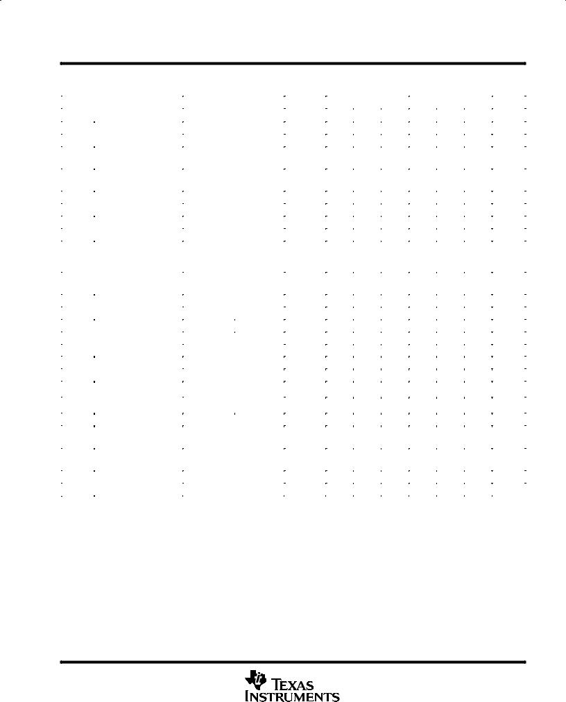
VIO |
Input offset voltage |
RS = 50 Ω |
|
25°C |
|
60 |
300 |
|
200 |
800 |
µV |
|
|
|
|
|
|
|
|
|
|||||
|
Full range |
|
|
550 |
|
|
1000 |
|||||
|
|
|
|
|
|
|
|
|
|
|||
|
|
|
|
|
|
|
|
|
|
|
|
|
aV |
IO |
Temperature coeficient |
|
|
Full range |
|
0.4 |
2.5 |
|
0.7 |
5 |
µV/°C |
|
of input offset voltage |
|
|
|
|
|
|
|
|
|
|
|
|
|
Long-term drift |
|
|
25°C |
|
0.5 |
|
|
0.5 |
|
µV/mo |
|
|
of input offset voltage |
|
|
|
|
|
|
||||
|
|
|
|
|
|
|
|
|
|
|
|
|
|
|
|
|
|
|
|
|
|
|
|
|
|
IIO |
Input offset current |
|
|
25°C |
|
0.15 |
1.5 |
|
0.15 |
1.5 |
nA |
|
|
|
|
|
|
|
|
|
|
||||
|
|
Full range |
|
|
2.8 |
|
|
2.8 |
||||
|
|
|
|
|
|
|
|
|
|
|||
|
|
|
|
|
|
|
|
|
|
|
|
|
IIB |
|
Input bias current |
|
|
25°C |
|
±12 |
±30 |
|
±12 |
±30 |
nA |
|
|
|
|
|
|
|
|
|
|
|||
|
|
|
Full range |
|
|
±38 |
|
|
±38 |
|||
|
|
|
|
|
|
|
|
|
|
|||
|
|
|
|
|
|
|
|
|
|
|
|
|
|
|
|
|
|
|
±15 |
±15.3 |
|
±15 |
±15.3 |
|
|
|
|
Common-mode |
|
|
25°C |
to |
to |
|
to |
to |
|
|
VICR |
|
|
|
13.5 |
13.8 |
|
13.5 |
13.8 |
|
V |
||
input voltage range |
|
|
|
|
|
|||||||
|
|
|
|
Full range |
±15 |
|
|
±15 |
|
|
|
|
|
|
|
|
|
|
|
|
|
|
|||
|
|
|
|
|
to 13 |
|
|
to 13 |
|
|
|
|
|
|
|
|
|
|
|
|
|
|
|
||
|
|
|
|
|
|
|
|
|
|
|
|
|
VOM |
Maximum peak output |
RL = 2 kΩ |
|
25°C |
±12.5 |
±14 |
|
±12.5 |
±14 |
|
V |
|
voltage swing |
|
Full range |
±12 |
|
|
±12 |
|
|
||||
|
|
|
|
|
|
|
|
|
||||
|
|
Large-signal differential |
VO = ±10 V, |
RL = 600 Ω |
25°C |
0.5 |
2 |
|
0.5 |
2 |
|
|
AVD |
|
|
25°C |
1.2 |
8 |
|
1.2 |
8 |
|
V/µV |
||
voltage amplification |
VO = ±10 V, |
RL = 2 kΩ |
|
|
||||||||
|
|
Full range |
0.7 |
|
|
0.7 |
|
|
|
|||
|
|
|
|
|
|
|
|
|
|
|||
|
|
|
|
|
|
|
|
|
|
|
|
|
CMRR |
Common-mode |
VIC = ±15 V to 13.5 V |
25°C |
97 |
117 |
|
97 |
117 |
|
dB |
||
rejection ratio |
VIC = ±15 V to 13 V |
Full range |
94 |
|
|
94 |
|
|
||||
|
|
|
|
|
|
|
||||||
kSVR |
Supply-voltage |
VCC± = ±2 V to ±18 V |
25°C |
100 |
117 |
|
100 |
117 |
|
dB |
||
rejection ratio |
|
|
|
|
|
|
|
|||||
Full range |
97 |
|
|
97 |
|
|
||||||
|
|
( VCC/ VIO) |
|
|
|
|
|
|
|
|||
|
|
Channel separation |
VO = ±10 V, |
RL = 2 kΩ |
25°C |
120 |
137 |
|
120 |
137 |
|
dB |
rid |
|
Differential |
|
|
25°C |
70 |
300 |
|
70 |
300 |
|
MΩ |
|
input resistance |
|
|
|
|
|||||||
|
|
|
|
|
|
|
|
|
|
|
|
|
|
|
|
|
|
|
|
|
|
|
|
|
|
ric |
|
Common-mode |
|
|
25°C |
|
4 |
|
|
4 |
|
GΩ |
|
input resistance |
|
|
|
|
|
|
|||||
|
|
|
|
|
|
|
|
|
|
|
|
|
|
|
|
|
|
|
|
|
|
|
|
|
|
ICC |
Supply current |
|
|
25°C |
|
0.35 |
0.55 |
|
0.35 |
0.55 |
mA |
|
per amplifier |
|
|
Full range |
|
|
0.6 |
|
|
0.6 |
|||
|
|
|
|
|
|
|
|
|
|
|||
|
|
|
|
|
|
|
|
|
|
|
|
|
² Full range is 0°C to 70°C.
³ All typical values are at TA = 25°C.
POST OFFICE BOX 655303 •DALLAS, TEXAS 75265 |
5 |

LT1014, LT1014A, LT1014D
QUAD PRECISION OPERATIONAL AMPLIFIERS
SLOS039C ± JULY 1989 ± REVISED SEPTEMBER 1999
electrical characteristics at specified free-air temperature, VCC± = 5 V, VCC± = 0, VO = 1.4 V, VIC = 0
(unless otherwise noted)
|
PARAMETER |
TEST CONDITIONS |
T ² |
|
LT1014C |
|
LT1014DC |
|
UNIT |
||
|
|
|
|
|
|
|
|||||
|
|
|
|
|
|
|
|||||
|
|
|
|
A |
MIN |
TYP |
MAX |
MIN |
TYP |
MAX |
|
|
|
|
|
|
|
||||||
VIO |
Input offset voltage |
RS = 50 Ω |
|
25°C |
|
90 |
450 |
|
250 |
950 |
µV |
|
Full range |
|
|
570 |
|
|
1200 |
||||
|
|
|
|
|
|
|
|
|
|||
|
|
|
|
|
|
|
|
|
|
|
|
IIO |
Input offset current |
|
|
25°C |
|
0.2 |
2 |
|
0.2 |
2 |
nA |
|
|
Full range |
|
|
6 |
|
|
6 |
|||
|
|
|
|
|
|
|
|
|
|||
|
|
|
|
|
|
|
|
|
|
|
|
IIB |
Input bias current |
|
|
25°C |
|
±15 |
±50 |
|
±15 |
±50 |
nA |
|
|
Full range |
|
|
±90 |
|
|
±90 |
|||
|
|
|
|
|
|
|
|
|
|||
|
|
|
|
|
|
|
|
|
|
|
|
|
Common-mode |
|
|
25°C |
0 |
±0.3 |
|
0 |
±0.3 |
|
|
VICR |
|
|
to 3.5 |
to 3.8 |
|
to 3.5 |
to 3.8 |
|
V |
||
input voltage range |
|
|
|
|
|
||||||
|
|
|
|
|
|
|
|
|
|||
|
|
Full range |
0 to 3 |
|
|
0 to 3 |
|
|
|
||
|
|
|
|
|
|
|
|
|
|||
|
|
|
|
|
|
|
|
|
|
|
|
|
|
Output low, |
No load |
25°C |
|
15 |
25 |
|
15 |
25 |
|
|
|
|
|
|
|
|
|
|
|
|
|
|
|
Output low, |
|
25°C |
|
5 |
10 |
|
5 |
10 |
mV |
|
Maximum peak output |
RL = 600 Ω to GND |
Full range |
|
|
13 |
|
|
13 |
||
|
|
|
|
|
|
||||||
VOM |
Output low, |
Isink = 1 mA |
25°C |
|
220 |
350 |
|
220 |
350 |
|
|
voltage swing |
|
|
|
||||||||
|
|
Output high, |
No load |
25°C |
4 |
4.4 |
|
4 |
4.4 |
|
|
|
|
|
|
|
|
|
|
|
|
|
|
|
|
Output high, |
|
25°C |
3.4 |
4 |
|
3.4 |
4 |
|
V |
|
|
RL = 600 Ω to GND |
Full range |
3.2 |
|
|
3.2 |
|
|
|
|
AVD |
Large-signal differential |
VO = 5 mV to 4 V, |
25°C |
|
1 |
|
|
1 |
|
V/µV |
|
voltage amplification |
RL = 500 Ω |
|
|
|
|
|
|||||
|
|
|
|
|
|
|
|
|
|
||
ICC |
Supply current |
|
|
25°C |
|
0.3 |
0.5 |
|
0.3 |
0.5 |
mA |
per amplifier |
|
|
Full range |
|
|
0.55 |
|
|
0.55 |
||
|
|
|
|
|
|
|
|
|
|||
|
|
|
|
|
|
|
|
|
|
|
|
² Full range is 0°C to 70°C.
operating characteristics, VCC± = ±15 V, VIC = 0, TA = 25°C
|
PARAMETER |
TEST CONDITIONS |
MIN |
TYP |
MAX |
UNIT |
||
|
|
|
|
|
|
|
|
|
SR |
Slew rate |
|
0.2 |
0.4 |
|
V/µs |
||
|
|
|
|
|
|
|
|
|
Vn |
Equivalent input noise voltage |
f = 10 Hz |
|
24 |
|
|
|
|
|
|
|
|
nV/√ |
Hz |
|
||
f = 1 kHz |
|
22 |
|
|
||||
|
|
|
|
|
|
|
||
|
|
|
|
|
|
|
||
VN(PP) |
Peak-to-peak equivalent input noise voltage |
f = 0.1 Hz to 10 Hz |
|
0.55 |
|
µV |
||
|
|
|
|
|
|
|
||
In |
Equivalent input noise current |
f = 10 Hz |
|
0.07 |
|
pA/√ |
Hz |
|
6 |
POST OFFICE BOX 655303 •DALLAS, TEXAS 75265 |

LT1014, LT1014A, LT1014D
QUAD PRECISION OPERATIONAL AMPLIFIERS
SLOS039C ± JULY 1989 ± REVISED SEPTEMBER 1999
electrical characteristics at specified free-air temperature, VCC± = ±15 V, VIC = 0 (unless otherwise noted)
|
|
PARAMETER |
TEST CONDITIONS |
T ² |
|
LT1014I |
|
|
LT1014DI |
|
UNIT |
|
|
|
|
|
|
|
|
|
|||||
|
|
|
|
|
|
|
|
|||||
|
|
|
|
|
A |
MIN |
TYP³ |
MAX |
MIN |
TYP³ |
MAX |
|
|
|
|
|
|
|
|
||||||
VIO |
Input offset voltage |
RS = 50 Ω |
|
25°C |
|
60 |
300 |
|
200 |
800 |
µV |
|
|
|
|
|
|
|
|
|
|||||
|
Full range |
|
|
550 |
|
|
1000 |
|||||
|
|
|
|
|
|
|
|
|
|
|||
|
|
|
|
|
|
|
|
|
|
|
|
|
aV |
IO |
Temperature coeficient |
|
|
Full range |
|
0.4 |
2.5 |
|
0.7 |
5 |
µV/°C |
|
of input offset voltage |
|
|
|
|
|
|
|
|
|
|
|
|
|
Long-term drift |
|
|
25°C |
|
0.5 |
|
|
0.5 |
|
µV/mo |
|
|
of input offset voltage |
|
|
|
|
|
|
||||
|
|
|
|
|
|
|
|
|
|
|
|
|
|
|
|
|
|
|
|
|
|
|
|
|
|
IIO |
Input offset current |
|
|
25°C |
|
0.15 |
1.5 |
|
0.15 |
1.5 |
nA |
|
|
|
|
|
|
|
|
|
|
||||
|
|
Full range |
|
|
2.8 |
|
|
2.8 |
||||
|
|
|
|
|
|
|
|
|
|
|||
|
|
|
|
|
|
|
|
|
|
|
|
|
IIB |
|
Input bias current |
|
|
25°C |
|
±12 |
±30 |
|
±12 |
±30 |
nA |
|
|
|
|
|
|
|
|
|
|
|||
|
|
|
Full range |
|
|
±38 |
|
|
±38 |
|||
|
|
|
|
|
|
|
|
|
|
|||
|
|
|
|
|
|
|
|
|
|
|
|
|
|
|
|
|
|
|
±15 |
±15.3 |
|
±15 |
±15.3 |
|
|
|
|
Common-mode |
|
|
25°C |
to |
to |
|
to |
to |
|
|
VICR |
|
|
|
13.5 |
13.8 |
|
13.5 |
13.8 |
|
V |
||
input voltage range |
|
|
|
|
|
|||||||
|
|
|
|
Full range |
±15 |
|
|
±15 |
|
|
|
|
|
|
|
|
|
|
|
|
|
|
|||
|
|
|
|
|
to 13 |
|
|
to 13 |
|
|
|
|
|
|
|
|
|
|
|
|
|
|
|
||
|
|
|
|
|
|
|
|
|
|
|
|
|
VOM |
Maximum peak |
RL = 2 kΩ |
|
25°C |
±12.5 |
±14 |
|
±12.5 |
±14 |
|
V |
|
output voltage swing |
|
Full range |
±12 |
|
|
±12 |
|
|
||||
|
|
|
|
|
|
|
|
|
||||
|
|
Large-signal differential |
VO = ±10 V, |
RL = 600 Ω |
25°C |
0.5 |
2 |
|
0.5 |
2 |
|
|
AVD |
|
|
25°C |
1.2 |
8 |
|
1.2 |
8 |
|
V/µV |
||
voltage amplification |
VO = ±10 V, |
RL = 2 kΩ |
|
|
||||||||
|
|
Full range |
0.7 |
|
|
0.7 |
|
|
|
|||
|
|
|
|
|
|
|
|
|
|
|||
|
|
|
|
|
|
|
|
|
|
|
|
|
CMRR |
Common-mode |
VIC = ±15 V to 13.5 V |
25°C |
97 |
117 |
|
97 |
117 |
|
dB |
||
rejection ratio |
Full range |
94 |
|
|
94 |
|
|
|||||
|
|
|
|
|
|
|
|
|
||||
|
|
|
|
|
|
|
|
|
|
|
|
|
kSVR |
Supply-voltage |
VCC± = ±2 V to ±18 V |
25°C |
100 |
117 |
|
100 |
117 |
|
dB |
||
rejection ratio |
|
|
|
|
|
|
|
|||||
Full range |
97 |
|
|
97 |
|
|
||||||
|
|
( VCC/ VIO) |
|
|
|
|
|
|
|
|||
|
|
Channel separation |
VO = ±10 V, |
RL = 2 kΩ |
25°C |
120 |
137 |
|
120 |
137 |
|
dB |
rid |
|
Differential |
|
|
25°C |
70 |
300 |
|
70 |
300 |
|
MΩ |
|
input resistance |
|
|
|
|
|||||||
|
|
|
|
|
|
|
|
|
|
|
|
|
|
|
|
|
|
|
|
|
|
|
|
|
|
ric |
|
Common-mode |
|
|
25°C |
|
4 |
|
|
4 |
|
GΩ |
|
input resistance |
|
|
|
|
|
|
|||||
|
|
|
|
|
|
|
|
|
|
|
|
|
|
|
|
|
|
|
|
|
|
|
|
|
|
ICC |
Supply current |
|
|
25°C |
|
0.35 |
0.55 |
|
0.35 |
0.55 |
mA |
|
per amplifier |
|
|
Full range |
|
|
0.6 |
|
|
0.6 |
|||
|
|
|
|
|
|
|
|
|
|
|||
|
|
|
|
|
|
|
|
|
|
|
|
|
² Full range is ±40°C to 105°C.
³ All typical values are at TA = 25°C.
POST OFFICE BOX 655303 •DALLAS, TEXAS 75265 |
7 |
LT1014, LT1014A, LT1014D
QUAD PRECISION OPERATIONAL AMPLIFIERS
SLOS039C ± JULY 1989 ± REVISED SEPTEMBER 1999
electrical characteristics at specified free-air temperature, VCC+ = 5 V, VCC± = 0, VO = 1.4 V, VIC = 0
(unless otherwise noted)
|
PARAMETER |
TEST CONDITIONS |
T ² |
|
LT1014I |
|
|
LT1014DI |
|
UNIT |
|
|
|
|
|
|
|
|
|||||
|
|
|
|
|
|
|
|||||
|
|
|
|
A |
MIN |
TYP |
MAX |
MIN |
TYP |
MAX |
|
|
|
|
|
|
|
||||||
|
|
|
|
|
|
|
|
|
|
|
|
VIO |
Input offset voltage |
RS = 50 Ω |
|
25°C |
|
90 |
450 |
|
250 |
950 |
µV |
|
|
|
|
|
|
|
|
||||
|
Full range |
|
|
570 |
|
|
1200 |
||||
|
|
|
|
|
|
|
|
|
|||
|
|
|
|
|
|
|
|
|
|
|
|
IIO |
Input offset current |
|
|
25°C |
|
0.2 |
2 |
|
0.2 |
2 |
nA |
|
|
|
|
|
|
|
|
|
|||
|
|
Full range |
|
|
6 |
|
|
6 |
|||
|
|
|
|
|
|
|
|
|
|||
|
|
|
|
|
|
|
|
|
|
|
|
IIB |
Input bias current |
|
|
25°C |
|
±15 |
±50 |
|
±15 |
±50 |
nA |
|
|
Full range |
|
|
±90 |
|
|
±90 |
|||
|
|
|
|
|
|
|
|
|
|||
|
|
|
|
|
|
|
|
|
|
|
|
|
Common-mode |
|
|
25°C |
0 |
±0.3 |
|
0 |
±0.3 |
|
|
VICR |
|
|
to 3.5 |
to 3.8 |
|
to 3.5 |
to 3.8 |
|
V |
||
input voltage range |
|
|
|
|
|
||||||
|
|
|
|
|
|
|
|
|
|||
|
|
Full range |
0 to 3 |
|
|
0 to 3 |
|
|
|
||
|
|
|
|
|
|
|
|
|
|||
|
|
|
|
|
|
|
|
|
|
|
|
|
|
Output low, |
No load |
25°C |
|
15 |
25 |
|
15 |
25 |
|
|
|
Output low, |
|
25°C |
|
5 |
10 |
|
5 |
10 |
mV |
|
Maximum peak |
RL = 600 Ω to GND |
Full range |
|
|
13 |
|
|
13 |
||
|
|
|
|
|
|
||||||
VOM |
Output low, |
Isink = 1 mA |
25°C |
|
220 |
350 |
|
220 |
350 |
|
|
output voltage swing |
|
|
|
||||||||
|
Output high, |
No load |
25°C |
4 |
4.4 |
|
4 |
4.4 |
|
|
|
|
|
|
|
|
|||||||
|
|
|
|
|
|
|
|
|
|
|
|
|
|
Output high, |
|
25°C |
3.4 |
4 |
|
3.4 |
4 |
|
V |
|
|
RL = 600 Ω to GND |
Full range |
3.2 |
|
|
3.2 |
|
|
|
|
AVD |
Large-signal differential |
VO = 5 mV to 4 V, |
25°C |
|
1 |
|
|
1 |
|
V/µV |
|
voltage amplification |
RL = 500 Ω |
|
|
|
|
|
|||||
ICC |
Supply current |
|
|
25°C |
|
0.3 |
0.5 |
|
0.3 |
0.5 |
mA |
per amplifier |
|
|
Full range |
|
|
0.55 |
|
|
0.55 |
||
|
|
|
|
|
|
|
|
|
|||
|
|
|
|
|
|
|
|
|
|
|
|
² Full range is ±40°C to 105°C.
operating characteristics, VCC+ = ±15 V, VIC = 0, TA = 25°C
|
PARAMETER |
TEST CONDITIONS |
MIN |
TYP |
MAX |
UNIT |
||
|
|
|
|
|
|
|
|
|
SR |
Slew rate |
|
0.2 |
0.4 |
|
V/µs |
||
Vn |
Equivalent input noise voltage |
f = 10 Hz |
|
24 |
|
|
|
|
|
|
|
|
nV/√ |
Hz |
|
||
f = 1 kHz |
|
22 |
|
|
||||
|
|
|
|
|
|
|
||
|
|
|
|
|
|
|
||
VN(PP) |
Peak-to-peak equivalent input noise voltage |
f = 0.1 Hz to 10 Hz |
|
0.55 |
|
µV |
||
|
|
|
|
|
|
|
||
In |
Equivalent input noise current |
f = 10 Hz |
|
0.07 |
|
pA/√ |
Hz |
|
8 |
POST OFFICE BOX 655303 •DALLAS, TEXAS 75265 |
 Loading...