


 Loading...
PRODUCT |
SAMPLE & |
TECHNICAL |
TOOLS & |
SUPPORT & |
FOLDER |
BUY |
DOCUMENTS |
SOFTWARE |
COMMUNITY |
LP2985-N
SNVS018X –MARCH 2000 –REVISED MAY 2015
LP2985-N Micropower 150-mA Low-Noise Ultra-Low-Dropout Regulator in SOT-23 and DSBGA Packages Designed for Use with Very Low ESR Output Capacitors
1 Features
•Input Voltage Range: 2.5 V to 16 V
•Ultra Low-Dropout Voltage
•Ensured 150 mA Output Current
•Smallest Possible Size (SOT-23 and DSBGA 0.5- mm Pitch Packages)
•Requires Minimum External Components
•Stable With Low-ESR Output Capacitor
•< 1 µA Quiescent Current When Shut Down
•Low Ground Pin Current at All Loads
•Output Voltage Accuracy 1% (A Grade)
•High Peak Current Capability
•Low ZOUT: 0.3 Ω Typical (10 Hz to 1 MHz)
•Overtemperature and Overcurrent Protection
•−40°C to 125°C Junction Temperature Range
•Custom Voltages Available
3 Description
The LP2985-N low noise linear regulator delivers up to 150-mA output current and only requires 300-mV dropout voltage of input to output. Using an optimized VIP (Vertically Integrated PNP) process, the LP2985- N delivers unequaled performance for all batterypowered designs. The LP2985-N device provides 1% tolerance precision output voltage with only 75 µA quiescent current at 1 mA load and 850 µA at 150 mA load. By adding a 10-nF bypass capacitor, the
output noise can be reduced to 30 µVRMS in a 30-kHz bandwidth.
The LP2985-N is designed to work with a ceramic output capacitor with equivalent series resistance (ESR) as low as 5 mΩ. The devices are available with fixed output voltage from 2.5 V to 6.1 V. Contact Texas Instrument Sales for specific voltage option needs.
The smallest SOT-23 and DSBGA packages are available for absolute minimum board space.
2 Applications
•Cellular Phone
•Palmtop and Laptop Computer
•Personal Digital Assistant (PDA)
•Camcorder, Personal Stereo, Camera
Device Information(1)
PART NUMBER |
PACKAGE |
BODY SIZE |
|
SOT-23 (5) |
2.90 mm x 1.60 mm (NOM) |
LP2985-N |
DSBGA (5) |
1.159 mm x 0.981 mm (MAX) |
|
1.464 mm x 1.095 mm (MAX) |
|
|
|
(1)For all available packages, see the orderable addendum at the end of the datasheet.
Simplified Schematic
VIN |
IN |
|
OUT |
VOUT |
CIN |
|
LP2985 |
COUT |
|
1 µF |
|
2.2 |
µF |
|
|
|
|||
|
GND |
|
|
|
ON/OFF |
|
ON/OFF BYPASS |
|
CBYPASS
 0.01 µF
An IMPORTANT NOTICE at the end of this data sheet addresses availability, warranty, changes, use in safety-critical applications, intellectual property matters and other important disclaimers. PRODUCTION DATA.

LP2985-N
SNVS018X –MARCH 2000 –REVISED MAY 2015 www.ti.com
Table of Contents
1 |
Features .................................................................. |
1 |
|
8.4 |
Device Functional Modes........................................ |
13 |
|
2 |
Applications ........................................................... |
1 |
9 |
Application and Implementation ........................ |
15 |
||
3 |
Description ............................................................. |
1 |
|
9.1 |
Application Information............................................ |
15 |
|
4 |
Revision History..................................................... |
2 |
|
9.2 |
Typical Application .................................................. |
15 |
|
5 |
Device Comparison Table..................................... |
3 |
10 |
Power Supply Recommendations ..................... |
22 |
||
6 |
Pin Configuration and Functions ......................... |
4 |
11 |
Layout................................................................... |
22 |
||
7 |
Specifications |
5 |
|
11.1 |
Layout Guidelines ................................................. |
22 |
|
|
11.2 |
Layout Example |
22 |
||||
|
7.1 |
Absolute Maximum Ratings |
5 |
|
|||
|
|
11.3 |
DSBGA Mounting |
22 |
|||
|
7.2 |
ESD Ratings |
5 |
|
|||
|
|
11.4 |
DSBGA Light Sensitivity |
23 |
|||
|
7.3 |
Recommended Operating Conditions |
5 |
|
|||
|
12 Device and Documentation Support |
24 |
|||||
|
7.4 |
Thermal Information .................................................. |
6 |
||||
|
7.5 |
Electrical Characteristics |
6 |
|
12.1 |
Documentation Support ........................................ |
24 |
|
|
12.2 |
Community Resources |
24 |
|||
|
7.6 |
Typical Characteristics |
8 |
|
|||
|
|
12.3 |
Trademarks |
24 |
|||
8 |
Detailed Description |
12 |
|
||||
|
12.4 |
Electrostatic Discharge Caution |
24 |
||||
|
8.1 |
Overview |
12 |
|
|||
|
|
12.5 |
Glossary |
24 |
|||
|
8.2 |
Functional Block Diagram |
12 |
|
|||
|
13 Mechanical, Packaging, and Orderable |
|
|||||
|
8.3 |
Feature Description................................................. |
12 |
24 |
|||
|
|
|
|
|
Information ........................................................... |
||
|
|
|
|
|
|
|
|
4 Revision History
NOTE: Page numbers for previous revisions may differ from page numbers in the current version.
Changes from Revision W (September 2014) to Revision X |
Page |
•Changed pin names in text and app circuit drawing "VOUT" and "VIN" to "OUT" and "IN"; replace Handling Ratings
|
with ESD Ratings; update Thermal Values ........................................................................................................................... |
1 |
• Changed footnote 1 to Ab Max table per new format ........................................................................................................... |
5 |
|
• |
Changed location of storage temperature range from Handling Ratings to Ab Max table..................................................... |
5 |
• |
Added required Application Information section .................................................................................................................. |
15 |
Changes from Revision V (April 2013) to Revision W |
Page |
|
•Added Pin Configuration and Functions section, Handling Rating table, Feature Description section, Device Functional Modes, Application and Implementation section, Power Supply Recommendations section, Layout section, Device and Documentation Support section, and Mechanical, Packaging, and Orderable Information
section ................................................................................................................................................................................... |
1 |
Changes from Revision U (April 2013) to Revision V |
Page |
• Changed layout of National Data Sheet to TI format ........................................................................................................... |
23 |
2 |
Submit Documentation Feedback |
Copyright © 2000–2015, Texas Instruments Incorporated |
Product Folder Links: LP2985-N

|
|
LP2985-N |
www.ti.com |
|
SNVS018X –MARCH 2000–REVISED MAY 2015 |
5 Device Comparison Table |
|
|
|
|
|
DEVICE NUMBER |
PACKAGE |
VOLTAGE OPTION (V) |
|
|
2.5 |
|
|
2.6 |
|
|
2.7 |
|
|
2.8 |
|
|
2.9 |
|
|
3.0 |
|
|
3.1 |
|
SOT-23 |
3.2 |
|
3.3 |
|
|
|
|
|
|
3.6 |
|
|
3.8 |
|
|
4.0 |
LP2985-N |
|
4.5 |
|
|
5.0 |
|
|
5.7 |
|
|
6.1 |
|
|
2.5 |
|
|
2.6 |
|
|
2.7 |
|
DSBGA (YPB) |
2.8 |
|
2.9 |
|
|
|
|
|
|
3.0 |
|
|
3.3 |
|
|
5.0 |
|
DSBGA (YZR) |
3.3 |
Copyright © 2000–2015, Texas Instruments Incorporated |
Submit Documentation Feedback |
3 |
Product Folder Links: LP2985-N

LP2985-N
SNVS018X –MARCH 2000 –REVISED MAY 2015 |
www.ti.com |
6 Pin Configuration and Functions
DBV Package
5 Pin SOT-23
Top View
YPB and YZR Packages
5-Pin DSBGA
Top View
|
|
|
Pin Functions |
||
|
PIN |
|
TYPE |
DESCRIPTION |
|
NAME |
SOT-23 |
DSBGA |
|||
|
|
||||
IN |
1 |
C3 |
I |
Input voltage |
|
GND |
2 |
A1 |
— |
Common ground (device substrate) |
|
ON/OFF |
3 |
A3 |
I |
Logic high enable input |
|
BYPASS |
4 |
B2 |
I/O |
Bypass capacitor for low noise operation |
|
OUT |
5 |
C1 |
O |
Regulated output voltage |
|
4 |
Submit Documentation Feedback |
Copyright © 2000–2015, Texas Instruments Incorporated |
Product Folder Links: LP2985-N

LP2985-N
www.ti.com |
SNVS018X –MARCH 2000–REVISED MAY 2015 |
7 |
Specifications |
|
|
|
7.1 |
Absolute Maximum Ratings |
|
|
|
over operating free-air temperature range (unless otherwise noted)(1)(2) |
|
|
|
|
|
|
MIN |
MAX |
UNIT |
Operating junction temperature |
–40 |
125 |
°C |
|
Lead Temp. (Soldering, 5 sec.) |
|
260 |
°C |
|
Power dissipation(3) |
Internally Limited |
|
||
Input supply voltage (survival) |
–0.3 |
16 |
V |
|
Input supply voltage (operating) |
2.5 |
16 |
V |
|
Shutdown input voltage (survival) |
–0.3 |
16 |
V |
|
Output voltage (survival, See(4)) |
–0.3 |
9 |
V |
|
IOUT (survival) |
Short Circuit Protected |
|
||
Input-output voltage (survival, see(5)) |
–0.3 |
16 |
V |
|
Storage temperature, Tstg |
–65 |
150 |
°C |
|
(1)Stresses beyond those listed under Absolute Maximum Ratings may cause permanent damage to the device. These are stress ratings only, which do not imply functional operation of the device at these or any other conditions beyond those indicated under Recommended Operating Conditions. Exposure to absolute-maximum-rated conditions for extended periods may affect device reliability.
(2)If Military/Aerospace specified devices are required, please contact the Texas Instruments Sales Office/ Distributors for availability and specifications.
(3)The maximum allowable power dissipation is a function of the maximum junction temperature, TJ_MAX, the junction-to-ambient thermal resistance, RθJA, and the ambient temperature, TA. The maximum allowable power dissipation at any ambient temperature is calculated using:
TJ _ MAX TA
PMAX
RTJA
Where the value of RθJA for the SOT-23 package is 175.7°C/W in a typical PC board mounting and 180°C/W for YZR type DSBGA package or 178.8°C/W for YPB type DSBGA package.
Exceeding the maximum allowable dissipation will cause excessive die temperature, and the regulator will go into thermal shutdown.
(4)For 12V option, output voltage survival: –0.3 to +16 V. If used in a dual-supply system where the regulator load is returned to a negative supply, the LP2985-N output must be diode-clamped to ground.
(5)The output PNP structure contains a diode between the IN to OUT pins that is normally reverse-biased. Reversing the polarity from IN to OUT will turn on this diode.
7.2 |
ESD Ratings |
|
|
|
|
|
|
|
|
VALUE |
UNIT |
|
|
|
All pins except 3 and 4 (SOT-23) |
|
|
|
|
Human-body model (HBM), per |
All pins except A3 and B2 |
±1000 |
|
V(ESD) |
Electrostatic discharge |
(DSBGA) |
|
V |
|
ANSI/ESDA/JEDEC JS-001(1) |
|
|
|||
Pins 1, 2, and 5 (SOT-23) |
±2000 |
||||
|
|
|
Pins A1, C1, and C3 (DSBGA) |
|
|
|
|
|
|
|
(1)JEDEC document JEP155 states that 500-V HBM allows safe manufacturing with a standard ESD control process.
7.3 Recommended Operating Conditions
over operating free-air temperature range (unless otherwise noted)
|
|
MIN |
MAX |
UNIT |
VIN |
Supply input voltage |
3.1(1) |
16 |
V |
VON/OFF |
ON/OFF input voltage |
0 |
VIN |
V |
IOUT |
Output current |
|
150 |
mA |
TJ |
Operating junction temperature |
–40 |
125 |
°C |
(1)Recommended minimum VIN is the greater of 3.1 V or VOUT(max) + rated dropout voltage (max) for operating load current.
Copyright © 2000–2015, Texas Instruments Incorporated |
Submit Documentation Feedback |
5 |
Product Folder Links: LP2985-N

LP2985-N
SNVS018X –MARCH 2000 –REVISED MAY 2015 www.ti.com
7.4 Thermal Information
|
|
|
LP2985-N |
|
|
|
THERMAL METRIC(1) |
SOT-23 |
DSBGA (YZR) |
DSBGA (YPB) |
UNIT |
|
|
|
5 PINS |
|
|
RθJA |
Junction-to-ambient thermal resistance |
175.7 |
180 |
178.8 |
|
RθJC(top) |
Junction-to-case (top) thermal resistance |
78 |
1 |
2.1 |
|
RθJB |
Junction-to-board thermal resistance |
30.8 |
109.3 |
146.3 |
°C/W |
ψJT |
Junction-to-top characterization parameter |
2.8 |
7.1 |
1.9 |
|
ψJB |
Junction-to-board characterization parameter |
30.3 |
109.3 |
146.3 |
|
(1)For more information about traditional and new thermal metrics, see the IC Package Thermal Metrics application report, SPRA953.
7.5 Electrical Characteristics
Unless otherwise specified: VIN = VO(NOM) + 1 V, IL = 1 mA, CIN = 1 µF, COUT = 4.7 µF, VON/OFF = 2 V, TJ = 25°C.(1)
|
|
PARAMETER |
TEST CONDITIONS |
TYP |
LP2985AI |
-X.X(2) |
LP2985I-X.X(2) |
UNIT |
||
|
|
MIN |
MAX |
MIN |
MAX |
|||||
|
|
|
|
|
|
|
||||
|
|
|
|
IL = 1 mA |
|
−1 |
1 |
–1.5 |
1.5 |
|
|
|
|
|
1 mA ≤ IL ≤ 50 mA |
|
−1.5 |
1.5 |
–2.5 |
2.5 |
|
VO |
|
|
|
1 mA ≤ IL ≤ 50 mA, –40°C ≤ TJ |
|
−2.5 |
2.5 |
–3.5 |
3.5 |
%VNOM |
|
|
Output voltage tolerance |
≤ 125°C |
|
|
|
|
|
||
|
|
|
|
1 mA ≤ IL ≤ 150 mA |
|
−2.5 |
2.5 |
–3 |
3 |
|
|
|
|
|
1 mA ≤ IL ≤ 150 mA, –40°C ≤ |
|
−3.5 |
3.5 |
–4 |
4 |
|
|
|
|
|
TJ ≤ 125°C |
|
|
|
|
|
|
VO/ |
VIN |
|
Output voltage |
VO(NOM)+1 V ≤ VIN ≤ 16 V |
0.007 |
|
0.014 |
|
0.014 |
%/V |
|
Line regulation |
VO(NOM)+1 V ≤ VIN ≤ 16 V, |
|
|
0.032 |
|
0.032 |
|||
|
|
|
|
–40°C ≤ TJ ≤ 125°C |
|
|
|
|
|
|
|
|
|
|
IL = 0 |
1 |
|
3 |
|
3 |
|
|
|
|
|
IL = 0, –40°C ≤ TJ ≤ 125°C |
|
|
5 |
|
5 |
|
|
|
|
|
IL = 1 mA |
7 |
|
10 |
|
10 |
|
|
|
|
|
IL = 1 mA, –40°C ≤ TJ ≤ 125°C |
|
|
15 |
|
15 |
|
|
|
|
|
IL = 10 mA |
40 |
|
60 |
|
60 |
|
V –V |
|
|
Dropout voltage(3) |
IL = 10 mA, –40°C ≤ TJ ≤ |
|
|
90 |
|
90 |
mV |
O |
|
125°C |
|
|
|
|
|
|||
IN |
|
|
|
|
|
|
|
|
||
|
|
|
|
IL = 50 mA |
120 |
|
150 |
|
150 |
|
|
|
|
|
IL = 50 mA, –40°C ≤ TJ ≤ |
|
|
225 |
|
225 |
|
|
|
|
|
125°C |
|
|
|
|
|
|
|
|
|
|
IL = 150 mA |
280 |
|
350 |
|
350 |
|
|
|
|
|
IL = 150 mA, –40°C ≤ TJ ≤ |
|
|
575 |
|
575 |
|
|
|
|
|
125°C |
|
|
|
|
|
|
(1)Exposing the DSBGA device to direct sunlight will cause misoperation. See DSBGA Light Sensitivity for additional information.
(2)Limits are 100% production tested at 25°C. Limits over the operating temperature range are ensured through correlation using Statistical Quality Control (SQC) methods. The limits are used to calculate TI's Average Outgoing Quality Level (AOQL).
(3)Dropout voltage is defined as the input to output differential at which the output voltage drops 100 mV below the value measured with a 1 V differential.
6 |
Submit Documentation Feedback |
Copyright © 2000–2015, Texas Instruments Incorporated |
Product Folder Links: LP2985-N

LP2985-N
www.ti.com |
SNVS018X –MARCH 2000–REVISED MAY 2015 |
Electrical Characteristics (continued)
Unless otherwise specified: VIN = VO(NOM) + 1 V, IL = 1 mA, CIN = 1 µF, COUT = 4.7 µF, VON/OFF = 2 V, TJ = 25°C.(1)
|
PARAMETER |
TEST CONDITIONS |
TYP |
LP2985AI |
-X.X(2) |
LP2985I-X.X(2) |
UNIT |
|
MIN |
MAX |
MIN MAX |
||||
|
|
|
|
|
|||
|
|
IL = 0 |
65 |
|
95 |
95 |
|
|
|
IL = 0, –40°C ≤ TJ ≤ 125°C |
|
|
125 |
125 |
|
|
|
IL = 1 mA |
75 |
|
110 |
110 |
|
|
|
IL = 1 mA, –40°C ≤ TJ ≤ 125°C |
|
|
170 |
170 |
|
|
|
IL = 10 mA |
120 |
|
220 |
220 |
|
|
|
IL = 10 mA, –40°C ≤ TJ ≤ |
|
|
400 |
400 |
|
|
|
125°C |
|
|
|
|
|
IGND |
Ground pin current |
IL = 50 mA |
350 |
|
600 |
600 |
µA |
IL = 50 mA, –40°C ≤ TJ ≤ |
|
|
1000 |
1000 |
|||
|
|
125°C |
|
|
|
|
|
|
|
IL = 150 mA |
850 |
|
1500 |
1500 |
|
|
|
IL = 150 mA, –40°C ≤ TJ ≤ |
|
|
2500 |
2500 |
|
|
|
125°C |
|
|
|
|
|
|
|
VON/OFF < 0.3 V |
0.01 |
|
0.8 |
0.8 |
|
|
|
VON/OFF < 0.15 V, –40°C ≤ TJ ≤ |
0.05 |
|
2 |
2 |
|
|
|
125°C |
|
|
|
|
|
|
|
High = O/P ON |
1.4 |
|
|
|
|
|
|
High = O/P ON, –40°C ≤ TJ ≤ |
|
1.6 |
|
1.6 |
|
V |
ON/OFF input voltage(4) |
125°C |
|
|
|
|
V |
|
|
|
|
|
|||
ON/OFF |
|
Low = O/P OFF |
0.55 |
|
|
|
|
|
|
|
|
|
|
||
|
|
Low = O/P OFF, –40°C ≤ TJ ≤ |
|
|
0.15 |
0.15 |
|
|
|
125°C |
|
|
|
|
|
|
|
VON/OFF = 0 |
0.01 |
|
|
|
|
|
|
VON/OFF = 0, –40°C ≤ TJ ≤ |
|
|
−2 |
−2 |
|
ION/OFF |
ON/OFF input current |
125°C |
|
|
|
|
µA |
VON/OFF = 5 V |
5 |
|
|
|
|||
|
|
|
|
|
|
||
|
|
VON/OFF = 5 V, –40°C ≤ TJ ≤ |
|
|
15 |
15 |
|
|
|
125°C |
|
|
|
|
|
|
Output noise voltage |
BW = 300 Hz to 50 kHz, |
|
|
|
|
|
en |
COUT = 10 µF |
30 |
|
|
|
µV |
|
(RMS) |
|
|
|
||||
|
CBYPASS = 10 nF |
|
|
|
|
|
|
|
|
|
|
|
|
|
|
VO/ VIN |
Ripple rejection |
f = 1 kHz, CBYPASS = 10 nF |
45 |
|
|
|
dB |
|
|
COUT = 10 µF |
|
|
|
||
|
|
|
|
|
|
|
|
IO(SC) |
Short circuit current |
RL = 0 (Steady State)(5) |
400 |
|
|
|
mA |
IO(PK) |
Peak output current |
VOUT ≥ Vo(NOM) –5% |
350 |
|
|
|
mA |
(4)The ON/OFF input must be properly driven to prevent possible misoperation. For details, refer to ON/OFF Input Operation.
(5)The LP2985-N has foldback current limiting which allows a high peak current when VOUT > 0.5 V, and then reduces the maximum output current as VOUT is forced to ground (see Typical Characteristics curves).
Copyright © 2000–2015, Texas Instruments Incorporated |
Submit Documentation Feedback |
7 |
Product Folder Links: LP2985-N
LP2985-N
SNVS018X –MARCH 2000 –REVISED MAY 2015 |
www.ti.com |
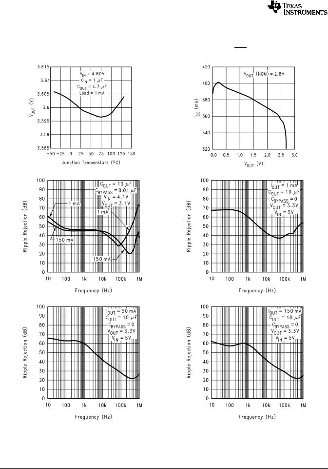
7.6 Typical Characteristics
Unless otherwise specified: CIN = 1 µF, COUT = 4.7 µF, VIN = VOUT(NOM) + 1, TA = 25°C, ON/OFF pin is tied to VIN.
Figure 1. VOUT vs Temperature |
Figure 2. Short Circuit Current vs Output Voltage |
|
|
Figure 3. Ripple Rejection |
Figure 4. Ripple Rejection |
|
|
Figure 5. Ripple Rejection |
Figure 6. Ripple Rejection |
|
|
8 |
Submit Documentation Feedback |
Copyright © 2000–2015, Texas Instruments Incorporated |
Product Folder Links: LP2985-N

LP2985-N
www.ti.com |
SNVS018X –MARCH 2000–REVISED MAY 2015 |
Typical Characteristics (continued)
Unless otherwise specified: CIN = 1 µF, COUT = 4.7 µF, VIN = VOUT(NOM) + 1, TA = 25°C, ON/OFF pin is tied to VIN.
Figure 7. Ripple Rejection |
Figure 8. Ripple Rejection |
|
|
Figure 9. Ripple Rejection |
Figure 10. Ripple Rejection |
|
|
Figure 11. Ripple Rejection |
Figure 12. Output Impedance vs Frequency |
|
|
Copyright © 2000–2015, Texas Instruments Incorporated |
Submit Documentation Feedback |
9 |
Product Folder Links: LP2985-N

LP2985-N
SNVS018X –MARCH 2000 –REVISED MAY 2015 |
www.ti.com |
Typical Characteristics (continued)
Unless otherwise specified: CIN = 1 µF, COUT = 4.7 µF, VIN = VOUT(NOM) + 1, TA = 25°C, ON/OFF pin is tied to VIN.
Figure 13. Output Impedance vs Frequency |
Figure 14. Output Noise Density |
|
|
Figure 15. Output Noise Density |
Figure 16. Ground Pin vs Load Current |
|
|
Figure 17. Dropout Voltage vs Temperature |
Figure 18. Input Current vs Pin |
|
|
10 |
Submit Documentation Feedback |
Copyright © 2000–2015, Texas Instruments Incorporated |
Product Folder Links: LP2985-N
LP2985-N
www.ti.com |
SNVS018X –MARCH 2000–REVISED MAY 2015 |
Typical Characteristics (continued)
Unless otherwise specified: CIN = 1 µF, COUT = 4.7 µF, VIN = VOUT(NOM) + 1, TA = 25°C, ON/OFF pin is tied to VIN.
Figure 19. GND Pin Current vs Temperature |
Figure 20. Instantaneous Short Circuit Current |
|
|
Copyright © 2000–2015, Texas Instruments Incorporated |
Submit Documentation Feedback |
11 |
Product Folder Links: LP2985-N

LP2985-N
SNVS018X –MARCH 2000 –REVISED MAY 2015 |
www.ti.com |
8 Detailed Description
8.1 Overview
The LP2985-N family of fixed-output, ultra-low-dropout and low-noise regulators offers exceptional, cost-effective performance for battery-powered applications. Available in output voltages from 2.5 V to 5 V, the family has an output tolerance of 1% for the A version (1.5% for the non-A version) and is capable of delivering 150-mA continuous load current. Standard regulator features, such as overcurrent and overtemperature protection, are also included.
Using an optimized Vertically Integrated PNP (VIP) process, the LP2985-N contains several features to facilitate battery powered designs:
•Multiple voltage options
•Low dropout voltage, typical dropout of 300 mV at 150 mA load current and 7 mV at 1 mA load.
•Low quiescent current and low ground current, typically 850-μA at 150 mA load, and 75-μA at 1-mA load.
•A shutdown feature is available, allowing the regulator to consume only 0.01-uA typically when the ON/OFF pin is pulled low.
•Over Temperature Protection and Over Current Protection circuitry is designed to safeguard the device during unexpected conditions
•Enhanced Stability: The LP2985-N is stable with output capacitor ESR as low as 5-mΩ, which allows the use of ceramic capacitors on the output.
•Low noise: A BYPASS pin allows for low-noise operation, with a typical output noise of 30 µVRMS, with the use of a 10-nF bypass capacitor.
8.2 Functional Block Diagram
8.3 Feature Description
8.3.1 Multiple Voltage Options
In order to meet different application’s requirement, the LP2985-N family provide multiple fixed output options from 2.5 V to 6.1 V. Please consult factory for custom voltages.
8.3.2 Output Voltage Accuracy
Output voltage accuracy specifies minimum and maximum output voltage error, relative to the expected nominal output voltage stated as a percent. This accuracy error includes the errors introduced by the internal reference and the load and line regulation across the full range of rated load and line operating conditions over temperature, unless otherwise specified by the Electrical Characteristics. Output voltage accuracy also accounts for all variations between manufacturing lots.
12 |
Submit Documentation Feedback |
Copyright © 2000–2015, Texas Instruments Incorporated |
Product Folder Links: LP2985-N

LP2985-N
www.ti.com |
SNVS018X –MARCH 2000–REVISED MAY 2015 |
Feature Description (continued)
8.3.3 Ultra-Low Dropout Voltage
Generally speaking, the dropout voltage often refers to the voltage difference between the input and output
voltage (VDO = VIN – VOUT), where the main current pass-FET is fully on in the ohmic region of operation and is characterized by the classic RDS(ON) of the FET. VDO indirectly specifies a minimum input voltage above the nominal programmed output voltage at which the output voltage is expected to remain within its accuracy
boundary. If the input falls below this VDO limit (VIN < VOUT + VDO), then the output voltage decreases in order to follow the input voltage.
8.3.4 Low Ground Current
LP2985-N uses a vertical PNP process which allows for quiescent currents that are considerably lower than those associated with traditional lateral PNP regulators, typically 850 μA at150 mA load, and 75 μA at 1-mA load.
8.3.5 Sleep Mode
When pull ON/OFF pin to low level, LP2985-N will enter sleep mode, and less than 2-μA quiescent current is consumed. This function is designed for the application which needs a sleep mode to effectively enhance battery life cycle.
8.3.6 Internal Protection Circuitry
8.3.6.1 Short Circuit Protection (Current Limit)
The internal current limit circuit is used to protect the LDO against high-load current faults or shorting events. The LDO is not designed to operate in a steady-state current limit. During a current-limit event, the LDO sources constant current. Therefore, the output voltage falls when load impedance decreases. Note also that if a current limit occurs and the resulting output voltage is low, excessive power may be dissipated across the LDO, resulting in a thermal shutdown of the output.
A fold back feature limits the short-circuit current to protect the regulator from damage under all load conditions. If VOUT is forced below 0 V before EN goes high and the load current required exceeds the fold back current limit, the device may not start up correctly.
8.3.6.2 Thermal Protection
The LP2985-N contains a thermal shutdown protection circuit to turn off the output current when excessive heat is dissipated in the LDO. The thermal time-constant of the semiconductor die is fairly short, and thus the output cycles on and off at a high rate when thermal shutdown is reached until the power dissipation is reduced.
The internal protection circuitry of the LP2985-N is designed to protect against thermal overload conditions. The circuitry is not intended to replace proper heat sinking. Continuously running the device into thermal shutdown degrades its reliability.
8.3.7 Enhanced Stability
The LP2985-N is designed specifically to work with ceramic output capacitors, utilizing circuitry which allows the regulator to be stable across the entire range of output current with an output capacitor whose ESR is as low as 5 mΩ. For output capacitor requirement, please refer to Output Capacitor.
8.3.8 Low Noise
The LP2985-N includes a low-noise reference ensuring minimal noise during operation because the internal reference is normally the dominant term in noise analysis. Further noise reduction can be achieved by adding an external bypass bapacitor between the BYPASS pin and the GND pin.
8.4 Device Functional Modes
8.4.1 Operation with VOUT(TARGET) + 0.6 V ≥ VIN > 16 V
The device operate if the input voltage is equal to, or exceeds VOUT(TARGET) + 0.6 V. At input voltages below the minimum VIN requirement, the devices do not operate correctly and output voltage may not reach target value.
Copyright © 2000–2015, Texas Instruments Incorporated |
Submit Documentation Feedback |
13 |
Product Folder Links: LP2985-N
Loading...