


|
|
OPA |
® |
|
|
||
|
|
||
|
|
|
4364 |
|
O |
|
|
|
PA |
|
|
|
|
43 |
64 |
OPA |
|
|
|
2364 |
|
|
|
OPA |
2363 |
|
|
|
|
|
|
|
OPA |
363 |
|
|
|
|
|
OPA363
OPA2363
OPA364
OPA2364
OPA4364
SBOS259B – SEPTEMBER 2002 – REVISED FEBRUARY 2003
1.8V, 7MHz, 90dB CMRR,
SINGLE-SUPPLY, RAIL-TO-RAIL I/O OPERATIONAL AMPLIFIER
FEATURES
●1.8V OPERATION
●MicroSIZE PACKAGES
●BANDWIDTH: 7MHz
●CMRR: 90dB (typical)
●SLEW RATE: 5V/ s
●LOW OFFSET: 500 V (max)
●QUIESCENT CURRENT: 750 A/Channel (max)
●SHUTDOWN MODE: < 1 A/Channel
APPLICATIONS
●SIGNAL CONDITIONING
●DATA ACQUISITION
●PROCESS CONTROL
●ACTIVE FILTERS
●TEST EQUIPMENT
|
OPA363 |
OPA364 |
OPA2363 |
OPA2364 |
OPA4364 |
|
|
|
|
|
|
SOT23-5 |
|
x |
|
|
|
|
|
|
|
|
|
SOT23-6 |
x |
|
|
|
|
|
|
|
|
|
|
MSOP-8 |
|
|
|
x |
|
|
|
|
|
|
|
MSOP-10 |
|
|
x |
|
|
|
|
|
|
|
|
SO-8 |
x |
x |
|
x |
|
|
|
|
|
|
|
TSSOP-14 |
|
|
|
|
x |
|
|
|
|
|
|
SO-14 |
|
|
|
|
x |
|
|
|
|
|
|
DESCRIPTION
The OPA363 and OPA364 families are high-performance CMOS operational amplifiers optimized for very low voltage, single-supply operation. These miniature, low-cost amplifiers are designed to operate on single supplies from 1.8V (± 0.9V) to 5.5V (± 2.75V). Applications include sensor amplification and signal conditioning in battery-powered systems.
The OPA363 and OPA364 families offer excellent CMRR without the crossover associated with traditional complimentary input stages. This results in excellent performance for driving Analog-to-Digital (A/D) converters without degradation of differential linearity and THD. The input commonmode range includes both the negative and positive supplies. The output voltage swing is within 10mV of the rails.
The OPA363 family includes a shutdown mode. Under logic control, the amplifiers can be switched from normal operation to a standby current that is less than 1 A.
The single version is available in the MicroSIZE SOT23-5 (SOT23-6 for shutdown) and SO-8. The dual version is available in MSOP-8, MSOP-10, and SO-8 packages. Quad packages are available in TSSOP-14 and SO-14 packages. All versions are specified for operation from –40° C to +125° C.
Please be aware that an important notice concerning availability, standard warranty, and use in critical applications of Texas Instruments semiconductor products and disclaimers thereto appears at the end of this data sheet.
PRODUCTION DATA information is current as of publication date. |
Copyright © 2002-2003, Texas Instruments Incorporated |
Products conform to specifications per the terms of Texas Instruments |
|
standard warranty. Production processing does not necessarily include |
|
testing of all parameters. |
|
www.ti.com

ABSOLUTE MAXIMUM RATINGS(1)
.................................................................................Supply Voltage |
+5.5V |
Signal Input Terminals, Voltage(2) ........................... |
–0.5V to (V+) + 0.5V |
Current(2) .................................................. |
± 10mA |
Enable Input ............................................................... |
(V–) – 0.5V to 5.5V |
Output Short-Circuit(3) .............................................................. |
Continuous |
Operating Temperature .................................................. |
–40° C to +150° C |
Storage Temperature ..................................................... |
–65° C to +150° C |
Junction Temperature .................................................................... |
+150° C |
Lead Temperature (soldering, 10s) ............................................... |
+300° C |
|
|
NOTES: (1) Stresses above these ratings may cause permanent damage. Exposure to absolute maximum conditions for extended periods may degrade device reliability. These are stress ratings only, and functional operation of the device at these or any other conditions beyond those specified is not implied. (2) Input terminals are diode-clamped to the power-supply rails. Input signals that can swing more than 0.5V beyond the supply rails should be current limited to 10mA or less. (3) Short-circuit to ground one amplifier per package.
ELECTROSTATIC DISCHARGE SENSITIVITY
This integrated circuit can be damaged by ESD. Texas Instruments recommends that all integrated circuits be handled with appropriate precautions. Failure to observe proper handling and installation procedures can cause damage.
ESD damage can range from subtle performance degradation to complete device failure. Precision integrated circuits may be more susceptible to damage because very small parametric changes could cause the device not to meet its published specifications.
PACKAGE/ORDERING INFORMATION
|
|
|
SPECIFIED |
|
|
|
|
|
PACKAGE |
TEMPERATURE |
PACKAGE |
ORDERING |
TRANSPORT |
PRODUCT |
PACKAGE-LEAD |
DESIGNATOR(1) |
RANGE |
MARKING |
NUMBER |
MEDIA, QUANTITY |
OPA363I |
SOT23-6 |
DBV |
–40° C to +125° C |
A40 |
OPA363IDBVT |
Tape and Reel, 250 |
" |
" |
" |
" |
" |
OPA363IDBVR |
Tape and Reel, 3000 |
|
|
|
|
|
|
|
OPA363I |
SO-8 |
D |
–40° C to +125° C |
OPA363 |
OPA363ID |
Rails, 100 |
" |
" |
" |
" |
" |
OPA363IDR |
Tape and Reel, 2500 |
|
|
|
|
|
|
|
OPA2363I |
MSOP-10 |
DGS |
–40° C to +125° C |
BHK |
OPA2363IDGST |
Tape and Reel, 250 |
" |
" |
" |
" |
" |
OPA2363IDGSR |
Tape and Reel, 2500 |
|
|
|
|
|
|
|
OPA364I |
SOT23-5 |
DBV |
–40° C to +125° C |
A41 |
OPA364IDBVT |
Tape and Reel, 250 |
" |
" |
" |
" |
" |
OPA364IDBVR |
Tape and Reel, 3000 |
|
|
|
|
|
|
|
OPA364I |
SO-8 |
D |
–40° C to +125° C |
OPA364 |
OPA364ID |
Rails, 100 |
" |
" |
" |
" |
" |
OPA364IDR |
Tape and Reel, 2500 |
|
|
|
|
|
|
|
OPA2364I |
MSOP-8 |
DGK |
–40° C to +125° C |
BHL |
OPA2364IDGKT |
Tape and Reel, 250 |
" |
" |
" |
" |
" |
OPA2364IDGKR |
Tape and Reel, 2500 |
|
|
|
|
|
|
|
OPA2364I |
SO-8 |
D |
–40° C to +125° C |
OPA2364 |
OPA2364ID |
Rails, 100 |
" |
" |
" |
" |
" |
OPA2364IDR |
Tape and Reel, 2500 |
|
|
|
|
|
|
|
OPA363AI |
SOT23-6 |
DBV |
–40° C to +125° C |
A40 |
OPA363AIDBVT |
Tape and Reel, 250 |
" |
" |
" |
" |
" |
OPA363AIDBVR |
Tape and Reel, 3000 |
|
|
|
|
|
|
|
OPA363AI |
SO-8 |
D |
–40° C to +125° C |
OPA363A |
OPA363AID |
Rails, 100 |
" |
" |
" |
" |
" |
OPA363AIDR |
Tape and Reel, 2500 |
|
|
|
|
|
|
|
OPA2363AI |
MSOP-10 |
DGS |
–40° C to +125° C |
BHK |
OPA2363AIDGST |
Tape and Reel, 250 |
" |
" |
" |
" |
" |
OPA2363AIDGSR |
Tape and Reel, 2500 |
|
|
|
|
|
|
|
OPA364AI |
SOT23-5 |
DBV |
–40° C to +125° C |
A41 |
OPA364AIDBVT |
Tape and Reel, 250 |
" |
" |
" |
" |
" |
OPA364AIDBVR |
Tape and Reel, 3000 |
|
|
|
|
|
|
|
OPA364AI |
SO-8 |
D |
–40° C to +125° C |
OPA364A |
OPA364AID |
Rails, 100 |
" |
" |
" |
" |
" |
OPA364AIDR |
Tape and Reel, 2500 |
|
|
|
|
|
|
|
OPA2364AI |
SO-8 |
D |
–40° C to +125° C |
OPA2634A |
OPA2364AID |
Rails, 100 |
" |
" |
" |
" |
" |
OPA2364AIDR |
Tape and Reel, 2500 |
|
|
|
|
|
|
|
OPA2364AI |
MSOP-8 |
DGK |
–40° C to +125° C |
BHL |
OPA2364AIDGKT |
Tape and Reel, 250 |
" |
" |
" |
" |
" |
OPA2364AIDGKR |
Tape and Reel, 2500 |
|
|
|
|
|
|
|
OPA4364AI |
SO-14 |
D |
–40° C to +125° C |
OPA4364A |
OPA4364AID |
Rails, 58 |
" |
" |
" |
" |
" |
OPA4364AIDR |
Tape and Reel, 2500 |
|
|
|
|
|
|
|
OPA4364AI |
TSSOP-14 |
PW |
–40° C to +125° C |
OPA4364A |
OPA4364AIPWT |
Tape and Reel, 250 |
" |
" |
" |
" |
" |
OPA4364AIPWR |
Tape and Reel, 2500 |
|
|
|
|
|
|
|
NOTES: (1) For the most current specifications and package information, refer to our web site at www.ti.com.
2 |
OPA363, 2363, 364, 2364, 4364 |
|
www.ti.com |
SBOS259B |
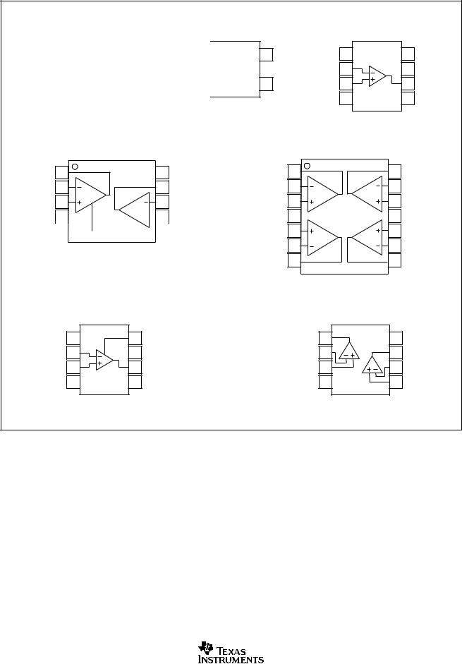
PIN CONFIGURATIONS
Top View
|
|
OPA363(1) |
|
|
|
|
|
|
|
|
|
V+ |
|
|
|
VOUT |
1 |
A40 |
6 |
VOUT |
1 |
||
V– |
2 |
5 |
Enable |
V– |
2 |
||
|
|||||||
|
|
|
|
–In |
|
|
|
|
|
|
|
|
|
||
+In |
3 |
|
4 |
+In |
3 |
||
|
|
|
|
|
|
|
|
|
|
|
|
|
|
|
|
|
|
SOT23-6 |
|
|
|
|
|
|
OPA2363 |
|
VOUT A |
1 |
10 |
+V |
–In A |
2 |
9 |
VOUT B |
|
|
A |
|
+In A |
3 |
8 |
–In B |
|
|
B |
|
–V |
4 |
|
|
|
|
|
|
7 |
+In B |
|
|
|
|
|
|
|
|
||||
|
|
|
|
|
|
|
|
|
|
Enable B |
|
|
|
|
|
|
|
|
|
|
|
Enable A |
5 |
|
|
|
|
|
|
|
6 |
|
|
|
|
|
|
|
|
||||
|
|
|
|
|
|
|
|
|
|
|
|
|
|
MSOP-10 |
|
||||||
OPA364(1)
5 V+
A41
4 –In
SOT23-5
VOUT A
–In A
+In A
V+
+In B
–In B
VOUT B
|
|
OPA364 |
|
|
NC |
1 |
|
8 |
NC |
–In |
2 |
|
7 |
V+ |
+In |
3 |
|
6 |
VOUT |
V– |
4 |
|
5 |
NC |
|
|
SO-8 |
|
|
OPA4364 |
|
|
|
|
1 |
|
14 |
VOUT D |
|
2 |
|
13 |
–In D |
|
A |
|
D |
|
|
3 |
|
12 |
+In D |
|
4 |
|
11 |
V– |
|
5 |
|
10 |
+In C |
|
B |
|
C |
|
|
6 |
|
9 |
–In C |
|
7 |
|
8 |
VOUT C |
|
SO-14, TSSOP-14
|
OPA363 |
NC |
1 |
–In |
2 |
+In |
3 |
V– |
4 |
|
SO-8 |
8 Enable
7 V+
6 VOUT
5 NC(1)
NOTE: (1) Orient according to marking.
NC = No Internal Connection.
|
|
OPA2364 |
|
Out A |
1 |
8 |
V+ |
–In A |
2 |
7 |
Out B |
+In A |
3 |
6 |
–In B |
V– |
4 |
5 |
+In B |
|
|
MSOP-8, SO-8 |
|
OPA363, 2363, 364, 2364, 4364 |
3 |
|
SBOS259B |
www.ti.com |

ELECTRICAL CHARACTERISTICS: VS = +1.8V to +5.5V
Boldface limits apply over the specified temperature range, TA = – 40° C to +125° C.
At TA = +25° C, RL = 10kΩ connected to VS /2, and VOUT = VS /2, VCM = VS /2, unless otherwise noted.
|
|
|
OPAx363, OPAx364 |
|
|
|
|
|
||||
|
|
|
|
|
|
|
|
|
|
|
|
|
PARAMETER |
|
CONDITION |
MIN |
TYP |
|
MAX |
UNITS |
|||||
|
|
|
|
|
|
|
|
|
|
|
|
|
OFFSET VOLTAGE |
|
|
|
|
|
|
|
|
|
|
|
|
Input Offset Voltage, OPA363I, OPA364I |
VOS |
VS = +5V |
|
|
|
500 |
µ V |
|||||
OPA2363I, OPA2364I |
|
|
|
|
|
900 |
µ V |
|||||
OPA363AI, OPA364AI, OPA2363AI, OPA2364AI, OPA4364AI |
|
|
|
1 |
2.5 |
mV |
||||||
Drift |
dVOS /dT |
|
|
|
3 |
|
|
µ V/°C |
||||
vs Power Supply |
PSRR |
VS = 1.8V to 5.5V, VCM = 0 |
|
|
80 |
330 |
µ V/V |
|||||
Channel Separation, dc |
|
|
|
|
1 |
|
|
µ V/V |
||||
|
|
|
|
|
|
|
|
|
|
|
|
|
INPUT BIAS CURRENT |
|
|
|
|
|
|
|
|
|
|
|
|
Input Bias Current |
IB |
|
|
|
± 1 |
± 10 |
pA |
|||||
over Temperature |
|
|
See |
Typical Characteristics |
|
|
|
|
|
|||
Input Offset Current |
IOS |
|
|
|
± 1 |
± 10 |
pA |
|||||
NOISE |
|
|
|
|
|
|
|
|
|
|
|
|
Input Voltage Noise, f = 0.1Hz to 10Hz |
en |
|
|
|
10 |
|
|
µ Vp-p |
||||
Input Voltage Noise Density, f = 10kHz |
en |
|
|
|
17 |
|
|
nV/√ |
Hz |
|
||
Input Current Noise Density, f = 10kHz |
in |
|
|
|
0.6 |
|
|
fA/√ |
Hz |
|
||
INPUT VOLTAGE RANGE |
|
|
|
|
|
|
|
|
|
|
|
|
Common-Mode Voltage Range |
VCM |
|
(V–) – 0.1 |
|
(V+) + 0.1 |
V |
||||||
Common-Mode Rejection Ratio |
CMRR |
(V– ) – 0.1V < VCM < (V+) + 0.1V |
74 |
|
90 |
|
|
dB |
||||
INPUT CAPACITANCE |
|
|
|
|
|
|
|
|
|
|
|
|
Differential |
|
|
|
|
2 |
|
|
pF |
||||
Common-Mode |
|
|
|
|
3 |
|
|
pF |
||||
|
|
|
|
|
|
|
|
|
|
|
|
|
OPEN-LOOP GAIN |
|
RL = 10kΩ , 100mV < VO < (V+) – 100mV |
|
|
|
|
|
|
|
|
|
|
Open-Loop Voltage Gain |
AOL |
|
94 |
|
100 |
|
|
dB |
||||
OPA4364AI |
|
|
90 |
|
|
|
|
dB |
||||
over Temperature |
|
VS = +1.8V to +5.5V |
86 |
|
|
|
|
dB |
||||
FREQUENCY RESPONSE |
|
CL = 100pF |
|
|
|
|
|
|
|
|
|
|
Gain Bandwidth Product |
GBW |
|
|
|
7 |
|
|
MHz |
||||
Slew Rate SR |
|
G = +1 |
|
|
5 |
|
|
V/µ s |
||||
Settling Time, 0.1% |
tS |
VS = +5V, 4V Step, G = +1 |
|
|
1 |
|
|
µ s |
||||
0.01% |
|
VS = +5V, 4V Step, G = +1 |
|
|
1.5 |
|
|
µ s |
||||
Overload Recovery Time |
|
VIN • Gain > VS |
|
|
0.8 |
|
|
µ s |
||||
Total Harmonic Distortion + Noise |
THD+N |
VS = +5V, G = +1, f = 20Hz to 20kHz |
|
|
0.002 |
|
|
% |
|
|
||
OUTPUT |
|
|
|
|
|
|
|
|
|
|
|
|
Voltage Output Swing from Rail |
|
RL = 10kΩ |
|
|
10 |
20 |
mV |
|||||
over Temperature |
|
RL = 10kΩ |
|
|
|
|
20 |
mV |
||||
|
|
|
|
|
||||||||
Short-Circuit Current |
ISC |
|
See |
Typical Characteristics |
mA |
|||||||
Capacitive Load Drive |
CLOAD |
|
See |
Typical Characteristics |
|
|
|
|
|
|||
SHUTDOWN (for OPAx363) |
|
|
|
|
|
|
|
|
|
|
|
|
tOFF |
|
|
|
|
1 |
|
|
µ s |
||||
(1) |
|
|
|
|
20 |
|
|
µ s |
||||
tON |
|
|
|
|
|
|
||||||
VL (shutdown) |
|
|
|
|
|
|
(V–) + 0.8 |
V |
||||
VH (amplifier is active) |
|
|
0.75 (V+) |
|
5.5 |
V |
||||||
IQSD |
|
|
|
|
|
0.9 |
µ A |
|||||
POWER SUPPLY |
|
|
|
|
|
|
|
|
|
|
|
|
Specified Voltage Range |
VS |
|
1.8 |
|
|
5.5 |
V |
|||||
Operating Voltage Range |
|
|
|
|
1.8 to 5.5 |
|
|
V |
||||
Quiescent Current (per amplifier) |
IQ |
VS = +1.8V |
|
|
650 |
750 |
µ A |
|||||
|
|
VS = +3.6V |
|
|
850 |
1000 |
µ A |
|||||
|
|
VS = +5.5V |
|
|
1.1 |
1.4 |
mA |
|||||
TEMPERATURE RANGE |
|
|
|
|
|
|
|
|
|
|
|
|
Specified Range |
|
|
–40 |
|
+125 |
° C |
||||||
Operating Range |
|
|
–40 |
|
+150 |
° C |
||||||
Storage Range |
θ JA |
|
–65 |
|
+150 |
° C |
||||||
Thermal Resistance |
|
|
|
|
|
|
° C/W |
|||||
SOT23-5, SOT23-6 |
|
|
|
|
200 |
|
|
|||||
MSOP-8, MSOP-10, SO-8 |
|
|
|
|
150 |
|
|
° C/W |
||||
TSSOP-14, SO-14 |
|
|
|
|
100 |
|
|
° C/W |
||||
|
|
|
|
|
|
|
|
|
|
|
|
|
NOTE: (1) Part is considered enabled when input offset voltage returns to specified range.
4 |
OPA363, 2363, 364, 2364, 4364 |
|
www.ti.com |
SBOS259B |

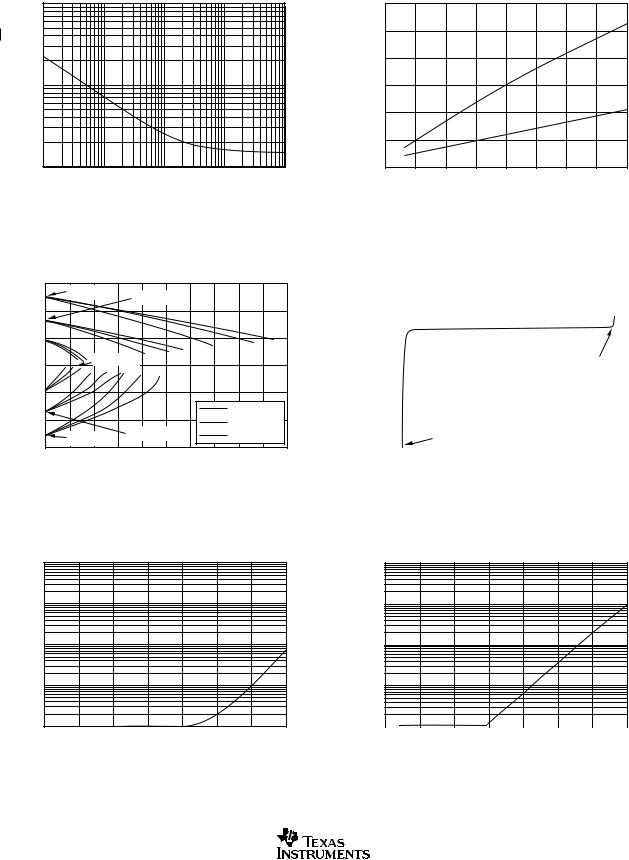
TYPICAL CHARACTERISTICS
At TCASE = +25° C, RL = 10kΩ , and connected to VS /2, VOUT = VS/2, VCM = VS/2, unless otherwise noted.
Voltage Gain (dB)
|
|
|
|
OPEN-LOOP GAIN/PHASE vs FREQUENCY |
|
|
|
||||||||||||||||||||||||||||
120 |
|
|
|
|
|
|
|
|
|
|
|
|
|
|
|
|
|
|
|
|
|
|
|
|
|
|
|
|
|
|
|
|
|
|
0 |
|
|
|
|
|
|
|
|
|
|
|
|
|
|
|
|
|
|
|
|
|
|
|
|
|
|
|
|
|
|
|
|
|
|
||
100 |
|
|
|
|
|
|
|
|
|
|
|
|
|
|
|
|
|
|
|
|
|
|
|
|
|
|
|
|
|
|
|
|
|
|
–30 |
|
|
|
|
|
|
|
|
|
|
|
|
|
|
|
|
|
|
|
|
|
|
|
|
|
|
|
|
|
|
|
|
|
|
||
80 |
|
|
|
|
|
|
|
|
|
|
|
|
|
|
|
|
|
|
|
|
|
|
|
|
|
|
|
|
|
|
|
|
|
|
–60 |
|
|
|
|
|
|
|
|
|
|
|
|
|
|
|
|
|
|
|
|
|
|
|
|
|
|
|
|
|
|
|
|
|
|
||
60 |
|
|
|
|
|
|
|
|
|
|
|
|
|
|
|
|
|
|
|
|
|
|
|
|
|
|
|
|
|
|
|
|
|
|
–90 |
|
|
|
|
|
|
|
|
|
|
|
|
|
|
|
|
|
|
|
|
|
|
|
|
|
|
|
|
|
|
|
|
|
|
||
40 |
|
|
|
|
|
|
|
|
|
|
|
|
|
|
|
|
|
|
|
|
|
|
|
|
|
|
|
|
|
|
|
|
|
|
–120 |
|
|
|
|
|
|
|
|
|
|
|
|
|
|
|
|
|
|
|
|
|
|
|
|
|
|
|
|
|
|
|
|
|
|
||
20 |
|
|
|
|
|
|
|
|
|
|
|
|
|
|
|
|
|
|
|
|
|
|
|
|
|
|
|
|
|
|
|
|
|
|
–150 |
|
|
|
|
|
|
|
|
|
|
|
|
|
|
|
|
|
|
|
|
|
|
|
|
|
|
|
|
|
|
|
|
|
|
||
0 |
|
|
|
|
|
|
|
|
|
|
|
|
|
|
|
|
|
|
|
|
|
|
|
|
|
|
|
|
|
|
|
|
|
|
–180 |
|
|
|
|
|
|
|
|
|
|
|
|
|
|
|
|
|
|
|
|
|
|
|
|
|
|
|
|
|
|
|
|
|
|
||
–20 |
|
|
|
|
|
|
|
|
|
|
|
|
|
|
|
|
|
|
|
|
|
|
|
|
|
|
|
|
|
|
|
|
|
|
|
|
|
|
|
|
|
|
|
|
|
|
|
|
|
|
|
|
|
|
|
|
|
|
|
|
|
|
|
|
|
|
|
|
|
|
|
10 |
|
100 |
|
|
1k |
|
|
10k |
100k |
1M |
10M |
100M |
|||||||||||||||||||||||
|
|
|
|
|
|
|
|
|
|
|
|
Frequency (Hz) |
|
|
|
|
|
|
|
|
|
|
|
|
|||||||||||
Phase (° )
CMRR (dB)
COMMON-MODE REJECTION RATIO vs FREQUENCY
100
90
80
70
60
50
40
30
20
10
0
10 |
100 |
1k |
10k |
100k |
1M |
10M |
|
|
|
Frequency (Hz) |
|
|
|
PSRR (dB)
POWER-SUPPLY REJECTION RATIO vs FREQUENCY
100
80
60
40
20
0
1 |
10 |
100 |
1k |
10k |
100k |
1M |
10M |
Frequency (Hz)
Quiescent Current (mA)
QUIESCENT CURRENT vs SUPPLY VOLTAGE
1.4
Per Amplifier
1.2
1.0
0.8
0.6
0.4
1.5 |
2.0 |
2.5 |
3.0 |
3.5 |
4.0 |
4.5 |
5.0 |
5.5 |
6.0 |
|
|
|
Supply Voltage (V) |
|
|
|
|||
TOTAL HARMONIC DISTORTION + NOISE vs FREQUENCY
|
1 |
VOUT = –10dBv |
G = 10, RL = 2kΩ |
|
|
|
|
|
|
|
|||
|
|
G = 10, RL = 2kΩ |
|
VS = 5V |
|
|
|
|
|
|
|
|
|
|
0.1 |
VS = 1.8V |
|
|
|
|
(%) |
|
|
|
|
|
|
THD+N |
0.01 |
G = 10, RL = 10kΩ |
|
|
||
|
VS = 1.8V, 5V |
|
|
|
||
|
|
|
|
|
|
|
|
0.001 |
G = 1, RL = 2kΩ |
|
|
G = 1, |
|
|
|
G = 1, |
|
RL = 10kΩ |
||
|
|
VS = 1.8V |
RL = 2kΩ |
VS = 1.8V, 5V |
||
|
0.0001 |
|
|
VS = 5V |
|
|
|
|
|
|
|
|
|
|
10 |
100 |
|
1k |
10k |
100k |
Frequency (Hz)
TOTAL HARMONIC DISTORTION + NOISE vs FREQUENCY
|
1 |
|
|
|
|
|
|
(VS = 5V, VOUT = 1Vrms) |
|
|
|
|
0.1 |
|
|
|
|
(%) |
|
G = 10, RL = 2kΩ |
|
|
|
|
|
|
|
|
|
THD+N |
0.01 |
|
|
|
|
|
G = 10, RL = 10kΩ |
|
|
|
|
|
0.001 |
|
|
|
|
|
|
G = 1, RL = 2kΩ |
|
G = 1, RL = 10kΩ |
|
|
0.0001 |
|
|
|
|
|
10 |
100 |
1k |
10k |
100k |
|
|
Frequency (Hz) |
|
||
OPA363, 2363, 364, 2364, 4364 |
5 |
|
SBOS259B |
www.ti.com |
TYPICAL CHARACTERISTICS (Cont.)
At TCASE = +25° C, RL = 10kΩ , and connected to VS /2, VOUT = VS/2, VCM = VS/2, unless otherwise noted.
Input Voltage Noise (nV/√ Hz)
INPUT VOLTAGE NOISE SPECTRAL DENSITY vs FREQUENCY
1000
100
10
10 |
100 |
1k |
10k |
100k |
Frequency (Hz)
Short-Circuit Current (mA)
SHORT-CIRCUIT CURRENT vs SUPPLY VOLTAGE
120
100
+ISC
80
60
40
–ISC
20
0
1.5 |
2.0 |
2.5 |
3.0 |
3.5 |
4.0 |
4.5 |
5.0 |
5.5 |
|
|
|
Supply Voltage (V) |
|
|
|
||
|
|
OUTPUT VOLTAGE SWING vs OUTPUT CURRENT |
|
|
|||||||
|
3 |
VS |
= ± 2.5V |
|
|
|
|
|
|
|
|
|
|
VS = ± 1.65V |
|
|
|
|
|
|
|
||
|
|
|
|
|
|
|
|
|
|
|
|
VoltageOutput(V) |
2 |
|
|
|
|
|
|
|
|
|
CurrentBiasInput(pA) |
1 |
|
|
|
|
|
TA = –40° C |
|
||||
|
|
|
|
|
|
|
|
|
|
|
|
|
0 |
|
VS = ± 0.9V |
|
|
|
|
|
|
|
|
|
|
|
|
|
|
|
|
|
|
|
|
|
–1 |
|
|
|
|
|
|
|
|
|
|
|
–2 |
|
|
VS = ± 1.65V |
|
|
TA = +25° C |
|
|
||
|
|
VS = ± 2.5V |
|
|
T |
A |
= +125° C |
|
|||
|
–3 |
|
|
|
|
|
|
|
|||
|
|
|
|
|
|
|
|
|
|
|
|
|
0 |
± 10 |
± 20 ± |
30 ± 40 ± 50 |
± 60 |
± 70 |
± |
80 ± 90 |
± |
100 |
|
|
|
|
|
Output Current (mA) |
|
|
|
|
|
||
INPUT BIAS CURRENT
vs INPUT COMMON-MODE VOLTAGE
4 |
|
|
|
|
|
|
|
|
|
|
|
|
|
|
|
|
|
|
|
|
|
|
|
|
|
|
|
|
|
|
|
2 |
|
|
|
|
|
|
|
|
|
|
|
|
|
|
|
|
|
|
|
|
|
|
|
|
|
|
|
|
|
|
|
0 |
|
|
|
|
|
|
|
|
|
|
|
|
|
|
|
|
|
|
|
|
|
|
|
|
|
|
|
|
|
|
|
–2 |
|
|
|
|
|
|
|
|
|
|
|
|
|
|
|
|
|
|
|
|
|
|
|
|
|
|
|
|
|
|
|
|
|
|
|
|
|
|
|
|
|
|
VCM |
= +5.1V |
|
|
|
–4 |
|
|
|
|
|
|
|
|
|
|
|
|
|
|
|
|
|
|
|
|
|
|
|
|
|
|
|
|
|
|
|
–6 |
|
|
|
|
|
|
|
|
|
|
|
|
|
|
|
|
|
|
|
|
|
|
|
|
|
|
|
|
|
|
|
–8 |
|
|
|
|
|
|
|
|
|
|
|
|
|
|
|
|
|
|
|
|
|
|
|
|
|
|
|
|
|
|
|
–10 |
|
|
|
|
VCM = –0.1V |
|
|
|
|
|
|
|
|
|
|
|
|
|
|
|
|
|
|
|
|
|
|
|
|
|
|
|
|
|
|
|
|
|
|
|
|
|
|
|
|
|
|
–0.5 |
0.5 |
1.5 |
2.5 |
3.5 |
4.5 |
5.5 |
|||||||||
|
|
|
|
|
Common-Mode Voltage (V) |
|
|
|
|
|
|||||
Input Offset Current (pA)
INPUT OFFSET CURRENT vs TEMPERATURE
10k
1k
100
10
1
–50 |
–25 |
0 |
25 |
50 |
75 |
100 |
125 |
|
|
|
Temperature (° C) |
|
|
|
|
Input Bias Current (pA)
INPUT BIAS CURRENT vs TEMPERATURE
10k
1k
100
10
1 |
|
|
|
|
|
|
|
|
|
|
|
|
|
|
|
|
|
|
|
–50 |
–25 |
0 |
25 |
50 |
75 |
100 |
125 |
||
|
|
|
|
Temperature (° C) |
|
|
|
|
|
6 |
OPA363, 2363, 364, 2364, 4364 |
|
www.ti.com |
SBOS259B |
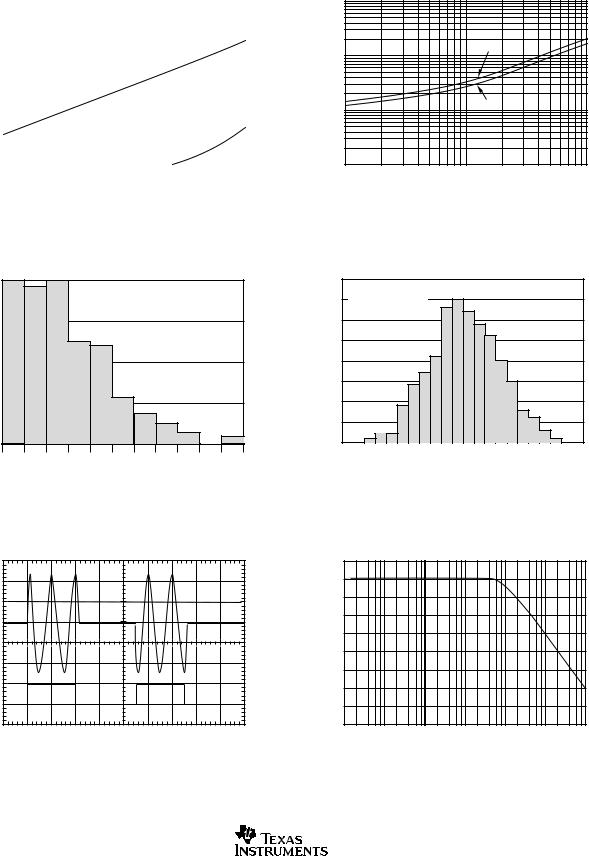
TYPICAL CHARACTERISTICS (Cont.)
At TCASE = +25° C, RL = 10kΩ , and connected to VS /2, VOUT = VS/2, VCM = VS/2, unless otherwise noted.
SMALL-SIGNAL OVERSHOOT vs LOAD CAPACITANCE
|
60 |
|
|
|
|
|
|
|
|
|
|
|
|
|
|
|
|
|
|
|
|
|
|
|
|
|
|
|
|
|
50 |
|
|
|
|
|
|
|
|
|
|
|
|
|
|
|
|
|
|
|
|
|
|
|
|
|
|
|
|
(%) |
40 |
|
|
|
|
|
|
|
|
|
|
|
|
|
|
|
|
|
|
|
|
|
|
|
|
|
|
||
|
|
|
|
|
|
|
|
|
|
|
|
|
|
|
Overshoot |
30 |
|
|
|
|
|
|
|
|
|
|
|
|
|
|
|
|
|
|
|
|
|
|
|
|
|
|
|
|
|
20 |
|
|
|
|
|
|
|
|
|
|
|
|
|
|
|
G = +1 |
|
|
|
|
|
|
|
|
|
|
|
|
|
|
|
|
|
|
|
|
|
|
|
|
|
|
|
|
10 |
|
|
|
|
|
|
|
|
|
|
|
|
|
|
|
|
|
|
|
|
|
|
|
|
|
|
|
|
|
|
|
|
|
|
|
G = +10 |
|
|
|
|
|
||
|
0 |
|
|
|
|
|
|
|
|
|
|
|
|
|
|
|
|
|
|
|
|
|
|
|
|
|
|
|
|
|
100 |
|
|
|
|
|
|
|
|
|
|
1k |
||
|
|
|
|
Load Capacitance (pF) |
||||||||||
OFFSET DRIFT DISTRIBUTION
|
20 |
|
|
|
|
|
|
|
|
|
(%) |
15 |
|
|
|
|
|
|
|
|
|
Amplifiers |
10 |
|
|
|
|
|
|
|
|
|
of |
|
|
|
|
|
|
|
|
|
|
Percent |
5 |
|
|
|
|
|
|
|
|
|
|
|
|
|
|
|
|
|
|
|
|
|
0 |
|
|
|
|
|
|
|
|
|
|
0 |
1 |
2 |
3 |
4 |
5 |
6 |
7 |
8 |
9 > 10 |
|
|
|
|
Offset Voltage Drift (µ V/° C) |
|
|
||||
SETTLING TIME vs CLOSED-LOOP GAIN
|
100 |
|
|
s) |
10 |
0.01% |
|
|
|
||
Time ( |
|
|
|
Settling |
1 |
0.1% |
|
|
|
||
|
|
|
|
|
0.1 |
|
|
|
1 |
10 |
100 |
|
|
Closed-Loop Gain (V/V) |
|
OFFSET VOLTAGE PRODUCTION DISTRIBUTION
|
16 |
Typical Production |
|
OPA36xAI |
|
|||
|
|
|
|
|||||
|
14 |
Distribution of |
|
|
|
|
|
|
(%) |
12 |
Packaged Units |
|
|
|
|
|
|
|
|
|
|
|
|
|
||
Amplifiers |
10 |
|
|
|
|
|
|
|
8 |
|
|
|
|
|
|
|
|
of |
6 |
|
|
|
|
|
|
|
Percent |
|
|
|
|
|
|
|
|
4 |
|
|
|
|
|
|
|
|
|
|
|
|
|
|
|
|
|
|
2 |
|
|
|
|
|
|
|
|
0 |
|
|
|
|
|
|
|
|
|
–2.5 |
–2.0 |
–1.0 |
0 |
1.0 |
2.0 |
2.5 |
Offset Voltage (mV)
V OUT
V ENABLE
OUTPUT ENABLE CHARACTERISTIC (VS = 5V, VOUT = 20kHz Sinusoid)
Channel Separation (dB)
50µ s/div
CHANNEL SEPARATION vs FREQUENCY
130
120
110
100
90
80
70
60
50
40
10 |
100 |
1k |
10k |
100k |
1M |
10M |
|
|
|
Frequency (Hz) |
|
|
|
OPA363, 2363, 364, 2364, 4364 |
7 |
|
SBOS259B |
www.ti.com |
 Loading...