


 Loading...
OMAP-L138
www.ti.com |
SPRS586B –JUNE 2009–REVISED AUGUST 2010 |
OMAP-L138 Low-Power Applications Processor
Check for Samples: OMAP-L138
1 OMAP-L138 Low-Power Applications Processor
1.1Features
• Highlights
– Dual Core SoC
• 375/456-MHz ARM926EJ-S™ RISC MPU
•375/456-MHz C674x Fixed/Floating-Point VLIW DSP
–Enhanced Direct-Memory-Access Controller (EDMA3)
–Serial ATA (SATA) Controller
–DDR2/Mobile DDR Memory Controller
–Two Multimedia Card (MMC)/Secure Digital (SD) Card Interface
–LCD Controller
–Video Port Interface (VPIF)
–10/100 Mb/s Ethernet MAC (EMAC):
–Programmable Real-Time Unit Subsystem
–Three Configurable UART Modules
–USB 1.1 OHCI (Host) With Integrated PHY
–USB 2.0 OTG Port With Integrated PHY
–One Multichannel Audio Serial Port
–Two Multichannel Buffered Serial Ports
•Dual Core SoC
–375/456-MHz ARM926EJ-S™ RISC MPU
–375/456-MHz C674x VLIW DSP
•ARM926EJ-S Core
–32-Bit and 16-Bit (Thumb® ) Instructions
–DSP Instruction Extensions
–Single Cycle MAC
–ARM® Jazelle® Technology
– EmbeddedICE-RT™ for Real-Time Debug
•ARM9 Memory Architecture
–16K-Byte Instruction Cache
–16K-Byte Data Cache
–8K-Byte RAM (Vector Table)
–64K-Byte ROM
•C674x Instruction Set Features
– Superset of the C67x+™ and C64x+™ ISAs
–Up to 3648/2746 C674x MIPS/MFLOPS
–Byte-Addressable (8-/16-/32-/64-Bit Data)
–8-Bit Overflow Protection
–Bit-Field Extract, Set, Clear
–Normalization, Saturation, Bit-Counting
–Compact 16-Bit Instructions
•C674x Two Level Cache Memory Architecture
–32K-Byte L1P Program RAM/Cache
–32K-Byte L1D Data RAM/Cache
–256K -Byte L2 Unified Mapped RAM/Cache
–Flexible RAM/Cache Partition (L1 and L2)
•Enhanced Direct-Memory-Access Controller 3 (EDMA3):
–2 Channel Controllers
–3 Transfer Controllers
–64 Independent DMA Channels
–16 Quick DMA Channels
–Programmable Transfer Burst Size
•TMS320C674x Floating-Point VLIW DSP Core
–Load-Store Architecture With Non-Aligned Support
–64 General-Purpose Registers (32 Bit)
–Six ALU (32-/40-Bit) Functional Units
•Supports 32-Bit Integer, SP (IEEE Single Precision/32-Bit) and DP (IEEE Double Precision/64-Bit) Floating Point
•Supports up to Four SP Additions Per Clock, Four DP Additions Every 2 Clocks
•Supports up to Two Floating Point (SP or DP) Reciprocal Approximation (RCPxP) and Square-Root Reciprocal Approximation (RSQRxP) Operations Per Cycle
–Two Multiply Functional Units
•Mixed-Precision IEEE Floating Point Multiply Supported up to:
–2 SP x SP -> SP Per Clock
–2 SP x SP -> DP Every Two Clocks
–2 SP x DP -> DP Every Three Clocks
–2 DP x DP -> DP Every Four Clocks
•Fixed Point Multiply Supports Two 32 x 32-Bit Multiplies, Four 16 x 16-Bit Multiplies, or Eight 8 x 8-Bit Multiplies per Clock Cycle, and Complex Multiples
–Instruction Packing Reduces Code Size
–All Instructions Conditional
Please be aware that an important notice concerning availability, standard warranty, and use in critical applications of Texas
 Instruments semiconductor products and disclaimers thereto appears at the end of this data sheet. TMS320C6000, C6000 are trademarks of Texas Instruments.
ARM926EJ-S is a trademark of ARM Limited.
ADVANCE INFORMATION concerns new products in the sampling |
Copyright © 2009–2010, Texas Instruments Incorporated |
or preproduction phase of development. Characteristic data and other |
|
specifications are subject to change without notice. |
|
ADVANCEINFORMATION

INFORMATIONADVANCE
OMAP-L138
SPRS586B –JUNE 2009 –REVISED AUGUST 2010 |
www.ti.com |
–Hardware Support for Modulo Loop Operation
–Protected Mode Operation
–Exceptions Support for Error Detection and Program Redirection
•Software Support
–TI DSP/BIOS™
–Chip Support Library and DSP Library
•128K-Byte RAM Shared Memory
•1.8V or 3.3V LVCMOS IOs (except for USB and DDR2 interfaces)
•Two External Memory Interfaces:
–EMIFA
•NOR (8-/16-Bit-Wide Data)
•NAND (8-/16-Bit-Wide Data)
•16-Bit SDRAM With 128 MB Address Space
–DDR2/Mobile DDR Memory Controller
•16-Bit DDR2 SDRAM With 512 MB Address Space or
•16-Bit mDDR SDRAM With 256 MB Address Space
•Three Configurable 16550 type UART Modules:
–With Modem Control Signals
–16-byte FIFO
–16x or 13x Oversampling Option
•LCD Controller
•Two Serial Peripheral Interfaces (SPI) Each With Multiple Chip-Selects
•Two Multimedia Card (MMC)/Secure Digital (SD) Card Interface with Secure Data I/O (SDIO) Interfaces
•Two Master/Slave Inter-Integrated Circuit (I2C Bus™ )
•One Host-Port Interface (HPI) With 16-Bit-Wide Muxed Address/Data Bus For High Bandwidth
•Programmable Real-Time Unit Subsystem (PRUSS)
–Two Independent Programmable Realtime Unit (PRU) Cores
•32-Bit Load/Store RISC architecture
•4K Byte instruction RAM per core
•512 Bytes data RAM per core
•PRU Subsystem (PRUSS) can be disabled via software to save power
•Register 30 of each PRU is exported from the subsystem in addition to the normal R31 output of the PRU cores.
–Standard power management mechanism
•Clock gating
•Entire subsystem under a single PSC clock gating domain
–Dedicated interrupt controller
–Dedicated switched central resource
•USB 1.1 OHCI (Host) With Integrated PHY (USB1)
•USB 2.0 OTG Port With Integrated PHY (USB0)
–USB 2.0 High-/Full-Speed Client
–USB 2.0 High-/Full-/Low-Speed Host
–End Point 0 (Control)
–End Points 1,2,3,4 (Control, Bulk, Interrupt or ISOC) Rx and Tx
•One Multichannel Audio Serial Port:
–Two Clock Zones and 16 Serial Data Pins
–Supports TDM, I2S, and Similar Formats
–DIT-Capable
–FIFO buffers for Transmit and Receive
•Two Multichannel Buffered Serial Ports:
–Supports TDM, I2S, and Similar Formats
–AC97 Audio Codec Interface
–Telecom Interfaces (ST-Bus, H100)
–128-channel TDM
–FIFO buffers for Transmit and Receive
•10/100 Mb/s Ethernet MAC (EMAC):
–IEEE 802.3 Compliant
–MII Media Independent Interface
–RMII Reduced Media Independent Interface
–Management Data I/O (MDIO) Module
•Video Port Interface (VPIF):
–Two 8-bit SD (BT.656), Single 16-bit or Single Raw (8-/10-/12-bit) Video Capture Channels
–Two 8-bit SD (BT.656), Single 16-bit Video Display Channels
•Universal Parallel Port (uPP):
–High-Speed Parallel Interface to FPGAs and Data Converters
–Data Width on Each of Two Channels is 8- to 16-bit Inclusive
–Single Data Rate or Dual Data Rate Transfers
–Supports Multiple Interfaces with START, ENABLE and WAIT Controls
•Serial ATA (SATA) Controller:
–Supports SATA I (1.5 Gbps) and SATA II (3.0 Gbps)
–Supports all SATA Power Management Features
–Hardware-Assisted Native Command Queueing (NCQ) for up to 32 Entries
–Supports Port Multiplier and Command-Based Switching
•Real-Time Clock With 32 KHz Oscillator and Separate Power Rail
•Three 64-Bit General-Purpose Timers (Each configurable as Two 32-Bit Timers)
•One 64-bit General-Purpose/Watchdog Timer (Configurable as Two 32-bit General-Purpose Timers)
2 OMAP-L138 Low-Power Applications Processor Copyright © 2009–2010, Texas Instruments Incorporated
Submit Documentation Feedback
Product Folder Link(s): OMAP-L138

OMAP-L138
www.ti.com |
SPRS586B –JUNE 2009–REVISED AUGUST 2010 |
•Two Enhanced Pulse Width Modulators (eHRPWM):
–Dedicated 16-Bit Time-Base Counter With Period And Frequency Control
–6 Single Edge, 6 Dual Edge Symmetric or 3 Dual Edge Asymmetric Outputs
–Dead-Band Generation
–PWM Chopping by High-Frequency Carrier
–Trip Zone Input
•Three 32-Bit Enhanced Capture Modules (eCAP):
–Configurable as 3 Capture Inputs or 3 Auxiliary Pulse Width Modulator (APWM)
outputs
–Single Shot Capture of up to Four Event Time-Stamps
•361-Ball Pb-Free Plastic Ball Grid Array (PBGA) [ZCE Suffix], 0.65-mm Ball Pitch
•361-Ball Pb-Free Plastic Ball Grid Array (PBGA) [ZWT Suffix], 0.80-mm Ball Pitch
•Commercial, Extended or Industrial Temperature
•Community Resources
–TI E2E Community
–TI Embedded Processors Wiki
ADVANCEINFORMATION
Copyright © 2009–2010, Texas Instruments Incorporated OMAP-L138 Low-Power Applications Processor 3
Submit Documentation Feedback
Product Folder Link(s): OMAP-L138

OMAP-L138
SPRS586B –JUNE 2009 –REVISED AUGUST 2010 |
www.ti.com |
1.2Trademarks
DSP/BIOS, TMS320C6000, C6000, TMS320, TMS320C62x, and TMS320C67x are trademarks of Texas Instruments.
All trademarks are the property of their respective owners.
INFORMATIONADVANCE
4 OMAP-L138 Low-Power Applications Processor Copyright © 2009–2010, Texas Instruments Incorporated
Submit Documentation Feedback
Product Folder Link(s): OMAP-L138

OMAP-L138
www.ti.com |
SPRS586B –JUNE 2009–REVISED AUGUST 2010 |
1.3Description
The device is a Low-power applications processor based on an ARM926EJ-S™ and a C674x DSP core. It provides significantly lower power than other members of the TMS320C6000™ platform of DSPs.
The device enables OEMs and ODMs to quickly bring to market devices featuring robust operating systems support, rich user interfaces, and high processing performance life through the maximum flexibility of a fully integrated mixed processor solution.
The dual-core architecture of the device provides benefits of both DSP and Reduced Instruction Set Computer (RISC) technologies, incorporating a high-performance TMS320C674x DSP core and an ARM926EJ-S core.
The ARM926EJ-S is a 32-bit RISC processor core that performs 32-bit or 16-bit instructions and processes 32-bit, 16-bit, or 8-bit data. The core uses pipelining so that all parts of the processor and memory system can operate continuously.
The ARM core has a coprocessor 15 (CP15), protection module, and Data and program Memory Management Units (MMUs) with table look-aside buffers. It has separate 16K-byte instruction and 16K-byte data caches. Both are four-way associative with virtual index virtual tag (VIVT). The ARM core also has a 8KB RAM (Vector Table) and 64KB ROM.
The device DSP core uses a two-level cache-based architecture. The Level 1 program cache (L1P) is a 32KB direct mapped cache and the Level 1 data cache (L1D) is a 32KB 2-way set-associative cache. The Level 2 program cache (L2P) consists of a 256KB memory space that is shared between program and data space. L2 memory can be configured as mapped memory, cache, or combinations of the two. Although the DSP L2 is accessible by ARM and other hosts in the system, an additional 128KB RAM shared memory is available for use by other hosts without affecting DSP performance.
The peripheral set includes: a 10/100 Mb/s Ethernet MAC (EMAC) with a Management Data Input/Output (MDIO) module; one USB2.0 OTG interface; one USB1.1 OHCI interface; two inter-integrated circuit (I2C) Bus interfaces; one multichannel audio serial port (McASP) with 16 serializers and FIFO buffers; two multichannel buffered serial ports (McBSP) with FIFO buffers; two SPI interfaces with multiple chip selects; four 64-bit general-purpose timers each configurable (one configurable as watchdog); a configurable 16-bit host port interface (HPI) ; up to 9 banks of 16 pins of general-purpose input/output (GPIO) with programmable interrupt/event generation modes, multiplexed with other peripherals; three UART interfaces (each with RTS and CTS); two enhanced high-resolution pulse width modulator (eHRPWM) peripherals; 3 32-bit enhanced capture (eCAP) module peripherals which can be configured as 3 capture inputs or 3 auxiliary pulse width modulator (APWM) outputs; and 2 external memory interfaces: an asynchronous and SDRAM external memory interface (EMIFA) for slower memories or peripherals, and a higher speed DDR2/Mobile DDR controller.
The Ethernet Media Access Controller (EMAC) provides an efficient interface between the device and a network. The EMAC supports both 10Base-T and 100Base-TX, or 10 Mbits/second (Mbps) and 100 Mbps in either halfor full-duplex mode. Additionally an Management Data Input/Output (MDIO) interface is available for PHY configuration. The EMAC supports both MII and RMII interfaces.
The SATA controller provides a high-speed interface to mass data storage devices. The SATA controller supports both SATA I (1.5 Gbps) and SATA II (3.0 Gbps).
The Universal Parallel Port (uPP) provides a high-speed interface to many types of data converters, FPGAs or other parallel devices. The UPP supports programmable data widths between 8- to 16-bits on each of two channels. Single-data rate and double-data rate transfers are supported as well as START, ENABLE and WAIT signals to provide control for a variety of data converters.
A Video Port Interface (VPIF) is included providing a flexible video input/output port.
The rich peripheral set provides the ability to control external peripheral devices and communicate with external processors. For details on each of the peripherals, see the related sections later in this document and the associated peripheral reference guides.
Copyright © 2009–2010, Texas Instruments Incorporated OMAP-L138 Low-Power Applications Processor 5
Submit Documentation Feedback
Product Folder Link(s): OMAP-L138
ADVANCEINFORMATION

OMAP-L138
SPRS586B –JUNE 2009 –REVISED AUGUST 2010 |
www.ti.com |
The device has a complete set of development tools for the ARM and DSP. These include C compilers, a DSP assembly optimizer to simplify programming and scheduling, and a Windows™ debugger interface for visibility into source code execution.
INFORMATIONADVANCE
6 OMAP-L138 Low-Power Applications Processor Copyright © 2009–2010, Texas Instruments Incorporated
Submit Documentation Feedback
Product Folder Link(s): OMAP-L138
OMAP-L138
www.ti.com |
SPRS586B –JUNE 2009–REVISED AUGUST 2010 |
1.4Functional Block Diagram
|
|
|
|
|
JTAG Interface |
ARM Subsystem |
DSP Subsystem |
|
|
|||||
|
|
System Control |
|
|
|
|
|
|
|
|
|
|
||
|
|
|
|
|
|
|
ARM926EJ-S CPU |
|
C674x™ |
|
|
|||
|
Input |
PLL/Clock |
|
|
|
With MMU |
|
DSP CPU |
|
|
||||
|
|
|
|
|
|
|
|
|
|
|
||||
|
Generator |
|
|
|
|
|
|
|
|
|
|
|||
|
Clock(s) |
|
|
|
|
|
|
|
|
|
|
|||
|
w/OSC |
|
|
|
|
|
|
|
|
|
|
|
||
|
|
|
|
|
|
4KB ETB |
|
AET |
|
|
||||
|
|
|
|
|
|
|
|
|
|
|||||
|
|
General- |
|
|
|
16KB |
16KB |
32KB |
32KB |
|
|
|||
|
|
Purpose |
|
|
|
|
|
|||||||
|
|
|
|
|
I-Cache |
D-Cache |
L1 Pgm |
L1 RAM |
|
|
||||
|
|
Timer (x3) |
Power/Sleep |
|
|
|
||||||||
|
|
|
|
|
|
|
|
|
|
|||||
|
|
|
|
|
Controller |
|
8KB RAM |
|
|
|
|
|
||
|
|
|
|
|
|
|
256KB L2 RAM |
|
|
|||||
|
|
RTC/ |
|
|
|
|
(Vector Table) |
|
|
|||||
|
|
|
|
Pin |
|
|
|
|
|
|
||||
|
|
32-kHz |
|
|
|
|
|
|
|
|
|
|
||
|
|
OSC |
|
Multiplexing |
|
64KB ROM |
|
BOOT ROM |
|
|
||||
|
|
|
|
|
Switched Central Resource (SCR) |
|
|
|
|
|||||
Peripherals |
|
|
|
|
|
|
|
|
|
|
|
|
||
DMA |
Audio Ports |
Serial Interfaces |
|
Display |
Video |
Parallel Port Internal Memory Customizable Interface |
||||||||
EDMA3 |
McASP |
McBSP |
I2C |
|
SPI |
UART |
LCD |
VPIF |
|
uPP |
128KB |
PRU Subsystem |
||
(x2) |
w/FIFO |
(x2) |
(x2) |
|
(x2) |
(x3) |
|
Ctlr |
|
RAM |
|
|||
|
|
|
|
|
|
|||||||||
Control Timers |
|
|
|
Connectivity |
|
|
|
|
External Memory Interfaces |
|||||
ePWM |
eCAP |
USB2.0 |
USB1.1 |
|
EMAC |
|
|
MMC/SD |
|
EMIFA(8b/16B) |
DDR2/MDDR |
|||
OTG Ctlr |
OHCI Ctlr |
10/100 |
MDIO |
HPI |
(8b) |
SATA |
NAND/Flash |
|||||||
(x2) |
(x3) |
Controller |
||||||||||||
PHY |
PHY |
|
(MII/RMII) |
|
|
(x2) |
|
|
16b SDRAM |
|||||
|
|
|
|
|
|
|
|
|||||||
(1)Note: Not all peripherals are available at the same time due to multiplexing.
Figure 1-1. Functional Block Diagram
ADVANCEINFORMATION
Copyright © 2009–2010, Texas Instruments Incorporated OMAP-L138 Low-Power Applications Processor 7
Submit Documentation Feedback
Product Folder Link(s): OMAP-L138

INFORMATIONADVANCE
OMAP-L138
SPRS586B –JUNE 2009 –REVISED AUGUST 2010 |
www.ti.com |
1 |
OMAP-L138 Low-Power Applications Processor |
1 |
|
|
............................................................... |
|
|
|
1.1 |
Features .............................................. |
1 |
|
1.2 |
Trademarks .......................................... |
4 |
|
1.3 |
Description ........................................... |
5 |
|
1.4 |
Functional Block Diagram ............................ |
7 |
2 |
Revision History ......................................... |
9 |
|
3 |
Device Overview ....................................... |
10 |
|
|
3.1 |
Documentation Support ............................ |
10 |
|
3.2 |
Device Characteristics .............................. |
10 |
|
3.3 |
Device Compatibility ................................ |
12 |
|
3.4 |
ARM Subsystem .................................... |
12 |
|
3.5 |
DSP Subsystem .................................... |
15 |
|
3.6 |
Memory Map Summary ............................. |
26 |
|
3.7 |
Pin Assignments .................................... |
29 |
|
3.8 |
Pin Multiplexing Control ............................ |
32 |
|
3.9 |
Terminal Functions ................................. |
33 |
|
3.10 |
Unused Pin Configurations ......................... |
74 |
4 |
Device Configuration ................................. |
77 |
|
|
4.1 |
Boot Modes ......................................... |
77 |
|
4.2 |
SYSCFG Module ................................... |
77 |
|
4.3 |
Pullup/Pulldown Resistors .......................... |
80 |
5 |
Device Operating Conditions ....................... |
81 |
|
5.1Absolute Maximum Ratings Over Operating Junction Temperature Range
(Unless Otherwise Noted) ................................. |
81 |
5.2 Recommended Operating Conditions .............. |
82 |
5.3Notes on Recommended Power-On Hours (POH)
...................................................... 84
5.4Electrical Characteristics Over Recommended Ranges of Supply Voltage and Operating Junction
Temperature (Unless Otherwise Noted) ............ |
85 |
6 Peripheral Information and Electrical |
|
Specifications .......................................... |
86 |
6.1 Parameter Information .............................. |
86 |
6.2Recommended Clock and Control Signal Transition
|
Behavior ............................................ |
87 |
6.3 |
Power Supplies ..................................... |
87 |
6.4 |
Reset ............................................... |
88 |
6.5 |
Crystal Oscillator or External Clock Input .......... |
91 |
|
6.6 |
|
Clock PLLs ......................................... |
92 |
6.7 |
|
Interrupts ............................................ |
97 |
6.8 |
Power and Sleep Controller (PSC) ................ |
107 |
|
6.9 |
|
EDMA ............................................. |
112 |
6.10 |
External Memory Interface A (EMIFA) ............ |
118 |
|
6.11 |
DDR2/mDDR Controller ........................... |
129 |
|
6.12 |
Memory Protection Units .......................... |
142 |
|
6.13 |
MMC / SD / SDIO (MMCSD0, MMCSD1) ......... |
145 |
|
6.14 |
Serial ATA Controller (SATA) ..................... |
148 |
|
6.15 |
Multichannel Audio Serial Port (McASP) .......... |
153 |
|
6.16 |
Multichannel Buffered Serial Port (McBSP) ....... |
162 |
|
6.17 |
Serial Peripheral Interface Ports (SPI0, SPI1) .... |
172 |
|
6.18 |
Inter-Integrated Circuit Serial Ports (I2C) ......... |
193 |
|
6.19Universal Asynchronous Receiver/Transmitter
(UART) ............................................ |
197 |
6.20Universal Serial Bus OTG Controller (USB0)
[USB2.0 OTG] ..................................... |
199 |
6.21Universal Serial Bus Host Controller (USB1)
|
[USB1.1 OHCI] .................................... |
206 |
6.22 |
Ethernet Media Access Controller (EMAC) ....... |
207 |
6.23 |
Management Data Input/Output (MDIO) .......... |
215 |
6.24 |
LCD Controller (LCDC) ............................ |
217 |
6.25 |
Host-Port Interface (UHPI) ........................ |
232 |
6.26 |
Universal Parallel Port (uPP) ...................... |
240 |
6.27 |
Video Port Interface (VPIF) ....................... |
245 |
6.28 |
Enhanced Capture (eCAP) Peripheral ............ |
251 |
6.29Enhanced High-Resolution Pulse-Width Modulator
|
(eHRPWM) ........................................ |
254 |
6.30 |
Timers ............................................. |
259 |
6.31 |
Real Time Clock (RTC) ........................... |
261 |
6.32 |
General-Purpose Input/Output (GPIO) ............ |
264 |
6.33Programmable Real-Time Unit Subsystem (PRUSS)
|
..................................................... |
268 |
6.34 |
Emulation Logic ................................... |
271 |
7 Mechanical Packaging and Orderable |
|
|
Information ............................................ |
280 |
|
7.1 |
Device Support .................................... |
280 |
7.2 |
Thermal Data for ZCE Package ................... |
282 |
7.3 |
Thermal Data for ZWT Package .................. |
283 |
8 Contents Copyright © 2009–2010, Texas Instruments Incorporated
Submit Documentation Feedback
Product Folder Link(s): OMAP-L138
OMAP-L138
www.ti.com |
SPRS586B –JUNE 2009–REVISED AUGUST 2010 |
2 Revision History
NOTE: This is a placeholder for the Revision History Table for future revisions of the document.
This data manual revision history highlights the changes made to the SPRS586A device-specific data manual to make it an SPRS586B revision.
Table 2-1. Revision History
ADDITIONS/MODIFICATIONS/DELETIONS
Global - Added MPU Content
Global - Replaced all "CLKIN" references with "OSCIN"
Global - Updated td(SCSL_SPC)S min from P to 2P
Global - Made changes in the document to reflect the following detail.
"The DSP L2 ROM is used for boot purposes and cannot be programmed with application code".
Global - Updated the pin map graphic to fix typos.
Global -
•All instances of EMU[0] updated to EMU0
•All instances of EMU[1] updated toEMU1
•All instances of UART1_RTS updated to have an overbar
•All instances of UART2_RTS updated to have an overbar
•All instances of SPI1_SCS[0] updated to have an overbar
•All instances of EMA_CS[4] updated to have an overbar
•All instances of SPI1_ENA updated to have an overbar
•All instances of SATA_TXN updated to have an overbar
•All instances of LCD_AC_ENB_CS updated to have an overbar
•All instances of DDR_CS updated to have an overbar
•All instances of UHPI_HRDY updated to have an overbar
•All instances of UHPI_HDS1 updated to have an overbar
•All instances of UHPI_HCS updated to have an overbar
Added Table 3-3 C674x L1/L2 Memory Protection Registers
Added Section 3.10 Unused Pin Configurations
Added Section 6.6.3- Dynamic Voltage and Frequency Scaling (DVFS)
AddedSection 4.3 Pullup/Pulldown Resistors
Added Section 6.14.3 - SATA Unused Signal Configuration
Added sections -Section 6.14.2 - SATA Interface, Section 6.14.2.1 - SATA Interface Schematic, Section 6.14.2.2 - Compatible SATA Components and Modes, Section 6.14.2.3 - PCB Stackup Specifications, Section 6.14.2.4 - Routing Specifications, Section 6.14.2.5 - Coupling Capacitors, Section 6.14.2.6 - SATA Interface Clock Source requirements,
Updated the Nomenclature Graphic in Section 7.1.2
ADVANCEINFORMATION
Copyright © 2009–2010, Texas Instruments Incorporated Revision History 9
Submit Documentation Feedback
Product Folder Link(s): OMAP-L138

INFORMATIONADVANCE
OMAP-L138
SPRS586B –JUNE 2009 –REVISED AUGUST 2010 |
www.ti.com |
3 Device Overview
3.1Documentation Support
3.1.1Related Documentation From Texas Instruments
The following documents are available on the Internet at www.ti.com. Tip: Enter the literature number in the search box provided at www.ti.com.
DSP Reference Guides
SPRUG82 TMS320C674x DSP Cache User's Guide. Explains the fundamentals of memory caches and describes how the two-level cache-based internal memory architecture in the TMS320C674x digital signal processor (DSP) can be efficiently used in DSP applications. Shows how to maintain coherence with external memory, how to use DMA to reduce memory latencies, and how to optimize your code to improve cache efficiency. The internal memory architecture in the C674x DSP is organized in a two-level hierarchy consisting of a dedicated program cache (L1P) and a dedicated data cache (L1D) on the first level. Accesses by the CPU to the these first level caches can complete without CPU pipeline stalls. If the data requested by the CPU is not contained in cache, it is fetched from the next lower memory level, L2 or external memory.
SPRUFE8 TMS320C674x DSP CPU and Instruction Set Reference Guide. Describes the CPU architecture, pipeline, instruction set, and interrupts for the TMS320C674x digital signal processors (DSPs). The C674x DSP is an enhancement of the C64x+ and C67x+ DSPs with added functionality and an expanded instruction set.
SPRUFK5 TMS320C674x DSP Megamodule Reference Guide. Describes the TMS320C674x digital signal processor (DSP) megamodule. Included is a discussion on the internal direct memory access (IDMA) controller, the interrupt controller, the power-down controller, memory protection, bandwidth management, and the memory and cache.
SPRUFK9 TMS320C674x/OMAP-L1x Processor Peripherals Overview Reference Guide. Provides an overview and briefly describes the peripherals available on the device.
SPRUGM7 OMAP-L138 Applications Processor System Reference Guide .
3.2Device Characteristics
Table 3-1 provides an overview of the device. The table shows significant features of the device, including the capacity of on-chip RAM, peripherals, and the package type with pin count.
10 Device Overview Copyright © 2009–2010, Texas Instruments Incorporated
Submit Documentation Feedback
Product Folder Link(s): OMAP-L138
|
|
OMAP-L138 |
|
|
www.ti.com |
|
SPRS586B –JUNE 2009–REVISED AUGUST 2010 |
|
|
|
Table 3-1. Characteristics of OMAP-L138 |
|
|
|
|
|
|
|
|
|
HARDWARE FEATURES |
OMAP-L138 |
|
|
|
|
|
|
|
|
DDR2/mDDR Controller |
DDR2, 16-bit bus width, up to 150 MHz |
|
|
|
Mobile DDR, 16-bit bus width, up to 133 MHz |
|
|
|
|
|
|
|
|
|
|
|
|
|
|
EMIFA |
Asynchronous (8/16-bit bus width) RAM, Flash, |
|
|
|
16-bit SDRAM, NOR, NAND |
|
|
|
|
|
|
|
|
|
|
|
|
|
|
Flash Card Interface |
MMC and SD cards supported. |
|
|
|
|
|
|
|
|
EDMA3 |
64 independent channels, 16 QDMA channels, |
|
|
|
2 channel controllers, 3 transfer controllers |
|
|
|
|
|
|
|
|
|
|
|
|
|
|
Timers |
4 64-Bit General Purpose (each configurable as 2 separate |
|
|
|
32-bit timers, one configurable as Watch Dog) |
|
|
|
|
|
|
|
|
|
|
|
|
|
|
UART |
3 (each with RTS and CTS flow control) |
|
|
|
|
|
|
|
|
SPI |
2 (Each with one hardware chip select) |
|
|
|
|
|
|
|
Peripherals |
I2C |
2 (both Master/Slave) |
|
|
Not all peripherals pins |
Multichannel Audio Serial Port [McASP] |
1 (each with transmit/receive, FIFO buffer, 16 serializers) |
|
|
|
|
|
|
|
are available at the |
Multichannel Buffered Serial Port [McBSP] |
2 (each with transmit/receive, FIFO buffer, 16) |
|
|
same time (for more |
|
|
|
|
10/100 Ethernet MAC with Management Data I/O |
1 (MII or RMII Interface) |
|
|
|
detail, see the Device |
|
|
||
|
|
|
|
|
Configurations section). |
eHRPWM |
4 Single Edge, 4 Dual Edge Symmetric, or |
|
ADVANCEINFORMATION |
|
2 Dual Edge Asymmetric Outputs |
|
||
|
|
|
||
|
|
|
|
|
|
|
|
|
|
|
eCAP |
3 32-bit capture inputs or 3 32-bit auxiliary PWM outputs |
|
|
|
|
|
|
|
|
USB 2.0 (USB0) |
High-Speed OTG Controller with on-chip OTG PHY |
|
|
|
|
|
|
|
|
USB 1.1 (USB1) |
Full-Speed OHCI (as host) with on-chip PHY |
|
|
|
|
|
|
|
|
General-Purpose Input/Output Port |
9 banks of 16-bit |
|
|
|
|
|
|
|
|
LCD Controller |
1 |
|
|
|
|
|
|
|
|
SATA Controller |
1 (Support both SATA I and SATAII) |
|
|
|
|
|
|
|
|
Universal Parallel Port (uPP) |
1 |
|
|
|
|
|
|
|
|
Video Port Interface (VPIF) |
1 (video in and video out) |
|
|
|
|
|
|
|
|
PRU Subsystem (PRUSS) |
2 Programmable PRU Cores |
|
|
|
|
|
|
|
|
Size (Bytes) |
488KB RAM |
|
|
|
|
|
|
|
|
|
DSP |
|
|
|
|
32KB L1 Program (L1P)/Cache (up to 32KB) |
|
|
|
|
32KB L1 Data (L1D)/Cache (up to 32KB) |
|
|
|
|
256KB Unified Mapped RAM/Cache (L2) |
|
|
|
|
DSP Memories can be made accessible to ARM, EDMA3, |
|
|
On-Chip Memory |
|
and other peripherals. |
|
|
Organization |
ARM |
|
|
|
|
|
|
||
|
|
16KB I-Cache |
|
|
|
|
16KB D-Cache |
|
|
|
|
8KB RAM (Vector Table) |
|
|
|
|
64KB ROM |
|
|
|
|
ADDITIONAL SHARED MEMORY |
|
|
|
|
128KB RAM |
|
|
|
|
|
|
|
C674x CPU ID + CPU |
Control Status Register (CSR.[31:16]) |
0x1400 |
|
|
Rev ID |
|
|
||
|
|
|
|
|
|
|
|
|
|
C674x Megamodule |
Revision ID Register (MM_REVID[15:0]) |
0x0000 |
|
|
Revision |
|
|
||
|
|
|
|
|
|
|
|
|
|
JTAG BSDL_ID |
DEVIDR0 Register |
0x0B7D_102F |
|
|
|
|
|
|
|
CPU Frequency |
MHz |
674x DSP 375 MHz (1.2V) or 456 MHz (1.3V) |
|
|
|
|
|
||
ARM926 375 MHz (1.2V) or 456 MHz (1.3V) |
|
|
||
|
|
|
|
|
|
|
|
|
|
|
Core (V) |
1.2 V nominal for 375 MHz version |
|
|
Voltage |
1.3 V nominal for 456 MHz version |
|
|
|
|
|
|
||
|
I/O (V) |
1.8V or 3.3 V |
|
|
|
|
|
|
|
Packages |
|
13 mm x 13 mm, 361-Ball 0.65 mm pitch, PBGA (ZCE) |
|
|
|
|
|
|
|
|
16 mm x 16 mm, 361-Ball 0.80 mm pitch, PBGA (ZWT) |
|
|
|
|
|
|
|
|
|
|
|
|
|
|
|
|
|
|
Copyright © 2009–2010, Texas Instruments Incorporated |
Device Overview |
11 |
|
|
|
Submit Documentation Feedback |
|
|
|
|
Product Folder Link(s): OMAP-L138 |
|
|
|

INFORMATIONADVANCE
OMAP-L138
SPRS586B –JUNE 2009 –REVISED AUGUST 2010 www.ti.com
|
Table 3-1. Characteristics of OMAP-L138 |
(continued) |
|
|
HARDWARE FEATURES |
|
OMAP-L138 |
|
|
|
|
Product Status(1) |
Product Preview (PP), |
|
375 MHz versions - PD |
Advance Information (AI), |
|
||
|
or Production Data (PD) |
|
456 MHz versions - AI |
|
|
|
|
|
|
|
|
(1)ADVANCE INFORMATION concerns new products in the sampling or preproduction phase of development. Characteristic data and other specifications are subject to change without notice. PRODUCTION DATA information is current as of publication date. Products conform to specifications per the terms of the Texas Instruments standard warranty. Production processing does not necessarily include testing of all parameters.
3.3Device Compatibility
The ARM926EJ-S RISC CPU is compatible with other ARM9 CPUs from ARM Holdings plc.
The C674x DSP core is code-compatible with the C6000™ DSP platform and supports features of both the C64x+ and C67x+ DSP families.
3.4ARM Subsystem
The ARM Subsystem includes the following features:
•ARM926EJ-S RISC processor
•ARMv5TEJ (32/16-bit) instruction set
•Little endian
•System Control Co-Processor 15 (CP15)
•MMU
•16KB Instruction cache
•16KB Data cache
•Write Buffer
•Embedded Trace Module and Embedded Trace Buffer (ETM/ETB)
•ARM Interrupt controller
3.4.1ARM926EJ-S RISC CPU
The ARM Subsystem integrates the ARM926EJ-S processor. The ARM926EJ-S processor is a member of ARM9 family of general-purpose microprocessors. This processor is targeted at multi-tasking applications where full memory management, high performance, low die size, and low power are all important. The ARM926EJ-S processor supports the 32-bit ARM and 16 bit THUMB instruction sets, enabling the user to trade off between high performance and high code density. Specifically, the ARM926EJ-S processor supports the ARMv5TEJ instruction set, which includes features for efficient execution of Java byte codes, providing Java performance similar to Just in Time (JIT) Java interpreter, but without associated code overhead.
The ARM926EJ-S processor supports the ARM debug architecture and includes logic to assist in both hardware and software debug. The ARM926EJ-S processor has a Harvard architecture and provides a complete high performance subsystem, including:
•ARM926EJ -S integer core
•CP15 system control coprocessor
•Memory Management Unit (MMU)
•Separate instruction and data caches
•Write buffer
•Separate instruction and data (internal RAM) interfaces
•Separate instruction and data AHB bus interfaces
•Embedded Trace Module and Embedded Trace Buffer (ETM/ETB)
12 Device Overview Copyright © 2009–2010, Texas Instruments Incorporated
Submit Documentation Feedback
Product Folder Link(s): OMAP-L138

OMAP-L138
www.ti.com |
SPRS586B –JUNE 2009–REVISED AUGUST 2010 |
For more complete details on the ARM9, refer to the ARM926EJ-S Technical Reference Manual, available at http://www.arm.com
3.4.2CP15
The ARM926EJ-S system control coprocessor (CP15) is used to configure and control instruction and data caches, Memory Management Unit (MMU), and other ARM subsystem functions. The CP15 registers are programmed using the MRC and MCR ARM instructions, when the ARM in a privileged mode such as supervisor or system mode.
3.4.3MMU
A single set of two level page tables stored in main memory is used to control the address translation, permission checks and memory region attributes for both data and instruction accesses. The MMU uses a single unified Translation Lookaside Buffer (TLB) to cache the information held in the page tables. The MMU features are:
•Standard ARM architecture v4 and v5 MMU mapping sizes, domains and access protection scheme.
•Mapping sizes are:
–1MB (sections)
–64KB (large pages)
–4KB (small pages)
–1KB (tiny pages)
•Access permissions for large pages and small pages can be specified separately for each quarter of the page (subpage permissions)
•Hardware page table walks
•Invalidate entire TLB, using CP15 register 8
•Invalidate TLB entry, selected by MVA, using CP15 register 8
•Lockdown of TLB entries, using CP15 register 10
3.4.4Caches and Write Buffer
The size of the Instruction cache is 16KB, Data cache is 16KB. Additionally, the caches have the following features:
•Virtual index, virtual tag, and addressed using the Modified Virtual Address (MVA)
•Four-way set associative, with a cache line length of eight words per line (32-bytes per line) and with two dirty bits in the Dcache
•Dcache supports write-through and write-back (or copy back) cache operation, selected by memory region using the C and B bits in the MMU translation tables
•Critical-word first cache refilling
•Cache lockdown registers enable control over which cache ways are used for allocation on a line fill, providing a mechanism for both lockdown, and controlling cache corruption
•Dcache stores the Physical Address TAG (PA TAG) corresponding to each Dcache entry in the TAG RAM for use during the cache line write-backs, in addition to the Virtual Address TAG stored in the TAG RAM. This means that the MMU is not involved in Dcache write-back operations, removing the possibility of TLB misses related to the write-back address.
•Cache maintenance operations provide efficient invalidation of, the entire Dcache or Icache, regions of the Dcache or Icache, and regions of virtual memory.
The write buffer is used for all writes to a noncachable bufferable region, write-through region and write misses to a write-back region. A separate buffer is incorporated in the Dcache for holding write-back for cache line evictions or cleaning of dirty cache lines. The main write buffer has 16-word data buffer and a four-address buffer. The Dcache write-back has eight data word entries and a single address entry.
ADVANCEINFORMATION
Copyright © 2009–2010, Texas Instruments Incorporated Device Overview 13
Submit Documentation Feedback
Product Folder Link(s): OMAP-L138

INFORMATIONADVANCE
OMAP-L138
SPRS586B –JUNE 2009 –REVISED AUGUST 2010 |
www.ti.com |
3.4.5Advanced High-Performance Bus (AHB)
The ARM Subsystem uses the AHB port of the ARM926EJ-S to connect the ARM to the Config bus and the external memories. Arbiters are employed to arbitrate access to the separate D-AHB and I-AHB by the Config Bus and the external memories bus.
3.4.6Embedded Trace Macrocell (ETM) and Embedded Trace Buffer (ETB)
To support real-time trace, the ARM926EJ-S processor provides an interface to enable connection of an Embedded Trace Macrocell (ETM). The ARM926ES-J Subsystem in the device also includes the Embedded Trace Buffer (ETB). The ETM consists of two parts:
•Trace Port provides real-time trace capability for the ARM9.
•Triggering facilities provide trigger resources, which include address and data comparators, counter, and sequencers.
The device trace port is not pinned out and is instead only connected to the Embedded Trace Buffer. The ETB has a 4KB buffer memory. ETB enabled debug tools are required to read/interpret the captured trace data.
3.4.7ARM Memory Mapping
By default the ARM has access to most on and off chip memory areas, including the DSP Internal memories, EMIFA, DDR2, and the additional 128K byte on chip shared SRAM. Likewise almost all of the on chip peripherals are accessible to the ARM by default.
See Table 3-4 for a detailed top level device memory map that includes the ARM memory space.
14 Device Overview Copyright © 2009–2010, Texas Instruments Incorporated
Submit Documentation Feedback
Product Folder Link(s): OMAP-L138
OMAP-L138
www.ti.com |
SPRS586B –JUNE 2009–REVISED AUGUST 2010 |
3.5DSP Subsystem
The DSP Subsystem includes the following features:
•C674x DSP CPU
•32KB L1 Program (L1P)/Cache (up to 32KB)
•32KB L1 Data (L1D)/Cache (up to 32KB)
•256KB Unified Mapped RAM/Cache (L2)
•Boot ROM (cannot be used for application code)
•Little endian
|
|
|
|
|
|
|
|
|
|
|
|
|
|
|
|
|
|
|
|
|
|
|
|
|
|
|
|
|
|
|
|
|
|
|
|
|
|
|
|
|
|
|
|
|
|
|
32K Bytes |
|
|
|
|
|
|
|
|
|
|
256K Bytes |
|
|
|
|
|
|
BOOT |
|
|||||||||
|
|
|
|
|
|
|
|
|
L1P RAM/ |
|
|
|
|
|
|
|
|
|
|
|
|
|
|
|
|
|
|||||||||||
|
|
|
|
|
|
|
|
|
|
|
|
|
|
|
|
|
|
|
|
|
L2 RAM |
|
|
|
|
|
|
ROM |
|
||||||||
|
|
|
|
|
|
|
|
|
Cache |
|
|
|
|
|
|
|
|
|
|
|
|
|
|
|
|
|
|
|
|||||||||
|
|
|
|
|
|
|
|
|
|
|
|
|
|
|
|
|
|
|
|
|
|
|
|
|
|
|
|
|
|
|
|
|
|
|
|||
|
|
|
|
|
|
|
|
|
|
|
|
|
|
|
|
|
|
|
|
|
|
|
|
|
|
|
|
|
|
|
|
|
|
||||
|
|
|
|
|
|
|
|
|
|
|
|
|
|
|
|
|
|
|
|
|
|
|
|
|
|
|
|
|
|
|
|
|
|
|
|
|
|
|
|
|
|
|
|
|
|
|
|
|
|
|
|
|
|
|
|
|
|
|
|
|
|
|
|
|
|
|
|
|
|
||||||
|
|
|
|
|
|
|
|
|
|
|
|
|
|
|
|
|
|
|
256 |
|
|
|
|
|
|
|
256 |
|
|
||||||||
|
|
|
|
|
256 |
|
|
|
|
|
|
|
|
|
|
|
|
|
|
|
|
|
|
|
|
|
|||||||||||
|
|
|
|
|
|
|
|
|
|
|
|
|
|
|
|
|
|
|
|
|
|
|
|
|
|
|
|
|
|
|
|
|
|
|
|
|
|
|
|
|
|
|
|
|
|
|
|
|
|
|
|
|
|
256 |
|
|
|
|
|
|
|
|
|
|
|
|
|
|
|
|
|
|
|
||
|
|
|
|
|
|
|
|
|
|
|
|
|
|
|
|
|
|
|
|
|
|
|
|
|
|
|
|
|
|
|
|
|
|
|
|||
|
|
|
|
|
|
|
|
|
|
|
|
|
|
|
|
|
|
|
|
|
|
|
|
|
|
|
|
|
|
|
|
|
|
|
|||
|
|
|
Cache Control |
|
|
|
|
|
|
|
Cache Control |
|
|
|
|
|
|||||||||||||||||||||
|
|
|
|
|
|
|
|
|
|
|
|
|
|
|
|
|
|
|
|
|
|
|
|||||||||||||||
|
|
|
|
|
|
|
|
|
|
|
|
|
|
|
|
|
|
|
|
|
|
|
|
|
|
|
|
|
|
|
|
|
|
|
|
|
|
|
|
|
Memory Protect |
|
|
L1P |
|
|
|
|
|
|
|
|
|
|
Memory Protect |
L2 |
|
|
|
||||||||||||||||
|
|
|
|
|
|
|
|
|
|
|
|
|
|
|
|
|
|
||||||||||||||||||||
|
|
|
|
|
|
|
|
|
|
|
|
|
|
|
|
|
|
|
|
|
|
|
|
|
|
|
|
|
|
|
|
|
|
|
|
|
|
|
|
|
Bandwidth Mgmt |
|
|
|
|
|
|
|
|
|
|
|
|
|
|
|
Bandwidth Mgmt |
|
|
|
|
|
|||||||||||||
|
|
|
|
|
|
|
|
|
|
|
|
|
|
|
|
|
|
||||||||||||||||||||
|
|
|
|
|
|
|
|
|
|
|
|
|
|
|
|
|
|
|
|
|
|
|
|
|
|
|
|
|
|
|
|
|
|
|
|
|
|
|
|
|
|
|
|
|
|
|
|
|
|
|
|
|
|
|
|
|
|
|
|
|
|
|
|
|
|
|
|
|
|
|
|
|
|
|
|
|
|
|
|
|
|
|
|
|
|
256 |
|
|
256 |
|
|
|
|
|
|
|
|
|
|
|
|
|
|
|
|
|
|
|
|
||||
|
|
|
|
|
|
|
|
|
|
|
|
|
|
|
|
|
|
|
|
|
|
|
|
|
|
|
|
|
Power Down |
|
|
|
|||||
|
|
|
|
Instruction Fetch |
256 |
|
256 |
|
|
||||||||||||||||||||||||||||
|
|
|
|
|
|
|
|
|
|
|
|
|
|
|
|
||||||||||||||||||||||
|
|
|
|
|
|
|
|
|
|
|
|
|
|
|
|
|
|
|
|
|
|
|
|
|
|
|
|
|
|||||||||
|
Interrupt |
C674x |
Controller |
|
|
Fixed/Floating Point CPU |
|
|
IDMA |
|
|
Register |
|
|
|
Register |
256 |
|
|
|
|
|
|
|
|
|
|
|
|
|
|
|
|
|
|
|
|
|
|
|
|||||||||||||||||||
|
|
File A |
|
|
|
|
File B |
|
|
|
|
|
|
|
|
|
|
|
|
|
|
|
|
|
|
|
|
|
|
|
|||||||||||||||||||
|
|
|
|
|
|
|
|
|
|
|
|
|
|
|
|
|
|
|
|
|
|
|
|
|
|
|
|
|
|
|
|
|
|
|
|||||||||||||||
|
|
|
|
|
|
|
|
|
|
|
|
|
|
|
|
|
|
|
|
|
|
|
|
|
|
|
|
|
|
|
|
|
|
|
|
|
|
|
|
|
|
|
|
|
|
||||
|
|
|
|
|
|
|
|
|
|
|
|
|
64 |
|
|
|
|
|
|
|
|
|
|
|
|
|
|
|
|
|
|
|
|
|
|
|
|
|
|
|
|
|
|
||||||
|
|
64 |
|
|
|
|
|
|
|
|
|
|
|
|
|
|
|
|
|
|
|
|
|
|
|
|
|
|
|
|
|
|
|
|
|
|
|
|
|
|
|||||||||
|
|
Bandwidth Mgmt |
|
|
|
|
|
|
|
|
|
|
|
|
|
|
EMC |
|
|
|
CFG |
32 |
|
|
|
|
Configuration |
|
|
|
|||||||||||||||||||
|
|
|
|
|
|
|
|
|
|
|
|
|
|
|
|
|
|
|
|
|
|
|
|
|
|
|
|||||||||||||||||||||||
|
|
|
|
|
|
|
|
|
|
|
|
|
|
|
|
|
|
|
|
|
|
|
|
|
|
|
|
|
|
|
|
|
|
|
|
|
|
|
|
|
|||||||||
|
|
Memory Protect |
|
|
L1D |
|
|
|
|
|
|
|
|
|
|
|
|
|
|
|
|||||||||||||||||||||||||||||
|
|
|
|
|
|
|
|
|
|
|
|
|
|
|
|
|
|
|
|
|
|
|
|
|
|
|
|
Peripherals |
|
|
|
||||||||||||||||||
|
|
|
|
|
|
|
|
|
|
|
|
|
|
|
|
|
|
|
|
|
|
|
|
|
|
|
|
|
|
|
|
|
|
|
|
|
|
|
|
|
|
|
|
|
|
|
|
||
|
|
Cache Control |
|
|
|
|
|
|
|
|
|
|
|
|
|
|
|
|
|
|
|
|
|
|
|
|
|
|
|
|
|
|
|
Bus |
|
|
|
||||||||||||
|
|
|
|
|
|
|
|
|
|
|
|
|
|
|
|
|
|
|
|
|
|
|
|
|
|
|
|
||||||||||||||||||||||
|
|
|
|
|
|
|
|
|
|
|
|
|
MDMA |
|
SDMA |
|
|
|
|
|
|||||||||||||||||||||||||||||
|
|
|
|
|
|
|
|
|
|
|
|
|
|
|
|
|
|
|
|
|
|
|
|
|
|
|
|
|
|
|
|
|
|
|
|
|
|
|
|
|
|||||||||
|
|
|
|
|
|
|
|
|
|
|
|
|
|
|
|
|
|
|
|
|
|
|
|
|
|
|
|
|
|
|
|
|
|
|
|
|
|
|
|
|
|||||||||
|
|
|
|
|
|
|
|
|
|
|
|
|
|
|
|
|
|
|
|
|
|
|
|
|
|
|
|
|
|
|
|
|
|
|
|
|
|
|
|
|
|
|
|
|
|
|
|
|
|
|
|
|
|
|
|
|
|
|
|
|
|
|
|
|
|
|
|
|
|
|
|
|
|
|
|
|
|
|
|
|
|
|
|
|
|
|
|
|
|||||||||||
|
8 x 32 |
|
|
|
|
|
|
|
|
|
|
|
|
|
|
|
|
64 |
|
64 64 |
|
|
64 |
|
|
|
|
|
|
|
|
|
|
|
|
|
|
||||||||||||
|
|
|
|
|
|
|
|
|
|
|
|
|
|
|
|
|
|
|
|
|
|
|
|
|
|
|
|
|
|
|
|
|
|
|
|
|
|
|
|
|
|
|
|
|
|
|
|
|
|
|
|
|
|
|
|
|
32K Bytes |
|
|
|
|
|
|
|
|
|
|
|
|
|
High |
|
|
|
|
|
|
|
|
|
|
|
|
|
|
|
|
|
|
|
|||||||||
|
|
|
|
|
|
|
|
L1D RAM/ |
|
|
|
|
|
|
|
|
|
|
|
|
Performance |
|
|
|
|
|
|
|
|
|
|
|
|
|
|||||||||||||||
|
|
|
|
|
|
|
|
|
Cache |
|
|
|
|
|
|
|
|
|
|
|
|
Switch Fabric |
|
|
|
|
|
|
|
|
|
|
|
|
|
||||||||||||||
|
|
|
|
|
|
|
|
|
|
|
|
|
|
|
|
|
|
|
|
|
|
|
|
|
|
|
|
|
|
|
|
|
|
|
|
|
|
|
|
|
|
|
|
|
|
|
|
|
|
Figure 3-1. C674x Megamodule Block Diagram
ADVANCEINFORMATION
Copyright © 2009–2010, Texas Instruments Incorporated Device Overview 15
Submit Documentation Feedback
Product Folder Link(s): OMAP-L138

INFORMATIONADVANCE
OMAP-L138
SPRS586B –JUNE 2009 –REVISED AUGUST 2010 |
www.ti.com |
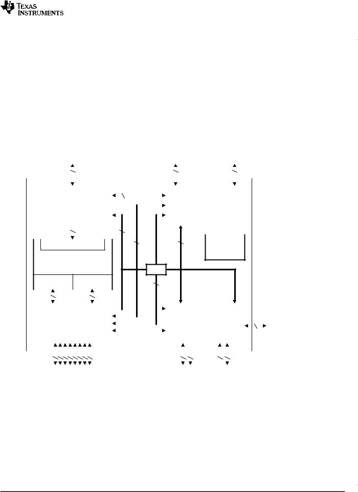
3.5.1C674x DSP CPU Description
The C674x Central Processing Unit (CPU) consists of eight functional units, two register files, and two data paths as shown in Figure 3-2. The two general-purpose register files (A and B) each contain 32 32-bit registers for a total of 64 registers. The general-purpose registers can be used for data or can be data address pointers. The data types supported include packed 8-bit data, packed 16-bit data, 32-bit data, 40-bit data, and 64-bit data. Values larger than 32 bits, such as 40-bit-long or 64-bit-long values are stored in register pairs, with the 32 LSBs of data placed in an even register and the remaining 8 or 32 MSBs in the next upper register (which is always an odd-numbered register).
The eight functional units (.M1, .L1, .D1, .S1, .M2, .L2, .D2, and .S2) are each capable of executing one instruction every clock cycle. The .M functional units perform all multiply operations. The .S and .L units perform a general set of arithmetic, logical, and branch functions. The .D units primarily load data from memory to the register file and store results from the register file into memory.
The C674x CPU combines the performance of the C64x+ core with the floating-point capabilities of the C67x+ core.
Each C674x .M unit can perform one of the following each clock cycle: one 32 x 32 bit multiply, one 16 x 32 bit multiply, two 16 x 16 bit multiplies, two 16 x 32 bit multiplies, two 16 x 16 bit multiplies with add/subtract capabilities, four 8 x 8 bit multiplies, four 8 x 8 bit multiplies with add operations, and four 16 x 16 multiplies with add/subtract capabilities (including a complex multiply). There is also support for Galois field multiplication for 8-bit and 32-bit data. Many communications algorithms such as FFTs and modems require complex multiplication. The complex multiply (CMPY) instruction takes for 16-bit inputs and produces a 32-bit real and a 32-bit imaginary output. There are also complex multiplies with rounding capability that produces one 32-bit packed output that contain 16-bit real and 16-bit imaginary values. The 32 x 32 bit multiply instructions provide the extended precision necessary for high-precision algorithms on a variety of signed and unsigned 32-bit data types.
The .L or (Arithmetic Logic Unit) now incorporates the ability to do parallel add/subtract operations on a pair of common inputs. Versions of this instruction exist to work on 32-bit data or on pairs of 16-bit data performing dual 16-bit add and subtracts in parallel. There are also saturated forms of these instructions.
The C674x core enhances the .S unit in several ways. On the previous cores, dual 16-bit MIN2 and MAX2 comparisons were only available on the .L units. On the C674x core they are also available on the .S unit which increases the performance of algorithms that do searching and sorting. Finally, to increase data packing and unpacking throughput, the .S unit allows sustained high performance for the quad 8-bit/16-bit and dual 16-bit instructions. Unpack instructions prepare 8-bit data for parallel 16-bit operations. Pack instructions return parallel results to output precision including saturation support.
Other new features include:
•SPLOOP - A small instruction buffer in the CPU that aids in creation of software pipelining loops where multiple iterations of a loop are executed in parallel. The SPLOOP buffer reduces the code size associated with software pipelining. Furthermore, loops in the SPLOOP buffer are fully interruptible.
•Compact Instructions - The native instruction size for the C6000 devices is 32 bits. Many common instructions such as MPY, AND, OR, ADD, and SUB can be expressed as 16 bits if the C674x compiler can restrict the code to use certain registers in the register file. This compression is performed by the code generation tools.
•Instruction Set Enhancement - As noted above, there are new instructions such as 32-bit multiplications, complex multiplications, packing, sorting, bit manipulation, and 32-bit Galois field multiplication.
•Exceptions Handling - Intended to aid the programmer in isolating bugs. The C674x CPU is able to detect and respond to exceptions, both from internally detected sources (such as illegal op-codes) and from system events (such as a watchdog time expiration).
•Privilege - Defines user and supervisor modes of operation, allowing the operating system to give a basic level of protection to sensitive resources. Local memory is divided into multiple pages, each with read, write, and execute permissions.
16 Device Overview Copyright © 2009–2010, Texas Instruments Incorporated
Submit Documentation Feedback
Product Folder Link(s): OMAP-L138

OMAP-L138
www.ti.com |
SPRS586B –JUNE 2009–REVISED AUGUST 2010 |
•Time-Stamp Counter - Primarily targeted for Real-Time Operating System (RTOS) robustness, a free-running time-stamp counter is implemented in the CPU which is not sensitive to system stalls.
For more details on the C674x CPU and its enhancements over the C64x architecture, see the following documents:
•TMS320C64x/C64x+ DSP CPU and Instruction Set Reference Guide (literature number SPRUFE8)
•TMS320C64x Technical Overview (literature number SPRU395)
ADVANCEINFORMATION
Copyright © 2009–2010, Texas Instruments Incorporated Device Overview 17
Submit Documentation Feedback
Product Folder Link(s): OMAP-L138

INFORMATIONADVANCE
OMAP-L138
SPRS586B –JUNE 2009 –REVISED AUGUST 2010 |
www.ti.com |
|
|
|
src1 |
|
|
|
.L1 |
src2 |
|
|
|
|
|
|
|
|
|
odd dst |
|
|
|
|
even dst |
|
|
|
32 MSB |
long src |
8 |
|
ST1b |
|
|
|
|
|
|
|
|
|
ST1a |
32 LSB |
|
|
|
|
|
8 |
|
|
|
|
long src |
|
|
|
|
|
|
|
|
|
even dst |
|
Data path A |
|
.S1 |
odd dst |
|
|
src1 |
|
||
|
|
|
|
|
|
|
|
src2 |
|
32
dst2
32
dst1
.M1 src1 src2
LD1b |
32 MSB |
|
32 LSB |
|
|
LD1a |
|
|
|
|
dst
.D1 src1
DA1
src2 
|
DA2 |
src2 |
|
|
.D2 |
src1 |
|
|
|
|
|
|
|
dst |
|
LD2a |
32 LSB |
|
|
32 MSB |
|
|
|
LD2b |
|
|
|
|
|
|
|
|
|
src2 |
|
|
.M2 |
src1 |
32 |
|
|
dst2 |
|
|
|
32 |
|
|
|
dst1 |
|
|
|
|
|
|
|
src2 |
|
|
|
src1 |
|
Data path B |
.S2 |
odd dst |
|
|
even dst |
8 |
|
|
|
long src |
|
|
|
|
|
ST2a |
32 MSB |
|
|
|
|
|
|
ST2b |
32 LSB |
|
|
|
|
|
|
|
|
long src |
8 |
|
|
|
|
|
|
even dst |
|
|
.L2 |
odd dst |
|
|
|
|
|
|
|
src1 |
|
Odd
Even
register
register
file A
file A
(A1, A3,
(A0, A2,
A5...A31)
A4...A30)
(D)
(D)
(A)
(B)
(C)
2x |
|
|
|
||
|
|
|
1x |
Even |
|
Odd |
register |
|
file B |
||
register |
||
(B0, B2, |
||
file B |
||
(B1, B3, |
B4...B30) |
|
|
||
B5...B31) |
|
(C)
(B)
(A)
(D)
(D)
Control Register
A.On .M unit, dst2 is 32 MSB.
B.On .M unit, dst1 is 32 LSB.
C.On C64x CPU .M unit, src2 is 32 bits; on C64x+ CPU .M unit, src2 is 64 bits.
D.On .L and .S units, odd dst connects to odd register files and even dst connects to even register files.
Figure 3-2. TMS320C674x CPU (DSP Core) Data Paths
18 Device Overview Copyright © 2009–2010, Texas Instruments Incorporated
Submit Documentation Feedback
Product Folder Link(s): OMAP-L138

OMAP-L138
www.ti.com |
SPRS586B –JUNE 2009–REVISED AUGUST 2010 |
3.5.2DSP Memory Mapping
The DSP memory map is shown in Section 3.6.
By default the DSP also has access to most on and off chip memory areas, with the exception of the ARM RAM, ROM, and AINTC interrupt controller.
Additionally, the DSP megamodule includes the capability to limit access to its internal memories through its SDMA port; without needing an external MPU unit.
3.5.2.1ARM Internal Memories
The DSP does not have access to the ARM internal memory.
3.5.2.2External Memories
The DSP has access to the following External memories:
•Asynchronous EMIF / SDRAM / NAND / NOR Flash (EMIFA)
•SDRAM (DDR2)
3.5.2.3DSP Internal Memories
The DSP has access to the following DSP memories:
•L2 RAM
•L1P RAM
•L1D RAM
3.5.2.4C674x CPU
The C674x core uses a two-level cache-based architecture. The Level 1 Program cache (L1P) is 32 KB direct mapped cache and the Level 1 Data cache (L1D) is 32 KB 2-way set associated cache. The Level 2 memory/cache (L2) consists of a 256 KB memory space that is shared between program and data space. L2 memory can be configured as mapped memory, cache, or a combination of both.
Table 3-2 shows a memory map of the C674x CPU cache registers for the device.
Table 3-2. C674x Cache Registers
Byte Address |
Register Name |
Register Description |
|
|
|
0x0184 0000 |
L2CFG |
L2 Cache configuration register |
|
|
|
0x0184 0020 |
L1PCFG |
L1P Size Cache configuration register |
|
|
|
0x0184 0024 |
L1PCC |
L1P Freeze Mode Cache configuration register |
|
|
|
0x0184 0040 |
L1DCFG |
L1D Size Cache configuration register |
|
|
|
0x0184 0044 |
L1DCC |
L1D Freeze Mode Cache configuration register |
|
|
|
0x0184 0048 - 0x0184 0FFC |
- |
Reserved |
|
|
|
0x0184 1000 |
EDMAWEIGHT |
L2 EDMA access control register |
|
|
|
0x0184 1004 - 0x0184 1FFC |
- |
Reserved |
|
|
|
0x0184 2000 |
L2ALLOC0 |
L2 allocation register 0 |
|
|
|
0x0184 2004 |
L2ALLOC1 |
L2 allocation register 1 |
|
|
|
0x0184 2008 |
L2ALLOC2 |
L2 allocation register 2 |
|
|
|
0x0184 200C |
L2ALLOC3 |
L2 allocation register 3 |
|
|
|
0x0184 2010 - 0x0184 3FFF |
- |
Reserved |
|
|
|
0x0184 4000 |
L2WBAR |
L2 writeback base address register |
|
|
|
0x0184 4004 |
L2WWC |
L2 writeback word count register |
|
|
|
0x0184 4010 |
L2WIBAR |
L2 writeback invalidate base address register |
|
|
|
0x0184 4014 |
L2WIWC |
L2 writeback invalidate word count register |
|
|
|
0x0184 4018 |
L2IBAR |
L2 invalidate base address register |
|
|
|
|
|
|
Copyright © 2009–2010, Texas Instruments Incorporated Device Overview 19
Submit Documentation Feedback
Product Folder Link(s): OMAP-L138
ADVANCEINFORMATION

OMAP-L138
SPRS586B –JUNE 2009 –REVISED AUGUST 2010 www.ti.com
Table 3-2. C674x Cache Registers (continued)
|
Byte Address |
Register Name |
Register Description |
|
|
|
|
|
|
|
0x0184 401C |
L2IWC |
L2 invalidate word count register |
|
|
|
|
|
|
|
0x0184 4020 |
L1PIBAR |
L1P invalidate base address register |
|
|
|
|
|
|
|
0x0184 4024 |
L1PIWC |
L1P invalidate word count register |
|
|
|
|
|
|
|
0x0184 4030 |
L1DWIBAR |
L1D writeback invalidate base address register |
|
|
|
|
|
|
|
0x0184 4034 |
L1DWIWC |
L1D writeback invalidate word count register |
|
|
|
|
|
|
|
0x0184 4038 |
- |
Reserved |
|
|
|
|
|
|
|
0x0184 4040 |
L1DWBAR |
L1D Block Writeback |
|
|
|
|
|
|
|
0x0184 4044 |
L1DWWC |
L1D Block Writeback |
|
|
|
|
|
|
|
0x0184 4048 |
L1DIBAR |
L1D invalidate base address register |
|
|
|
|
|
|
|
0x0184 404C |
L1DIWC |
L1D invalidate word count register |
|
|
|
|
|
|
|
0x0184 4050 - 0x0184 4FFF |
- |
Reserved |
|
|
|
|
|
|
|
0x0184 5000 |
L2WB |
L2 writeback all register |
|
|
|
|
|
|
|
0x0184 5004 |
L2WBINV |
L2 writeback invalidate all register |
|
|
|
|
|
|
|
0x0184 5008 |
L2INV |
L2 Global Invalidate without writeback |
|
|
|
|
|
|
ADVANCEINFORMATION |
0x0184 500C - 0x0184 5027 |
- |
Reserved |
|
|
|
|
||
0x0184 5028 |
L1PINV |
L1P Global Invalidate |
||
|
||||
|
|
|
|
|
|
0x0184 502C - 0x0184 5039 |
- |
Reserved |
|
|
|
|
|
|
|
0x0184 5040 |
L1DWB |
L1D Global Writeback |
|
|
|
|
|
|
|
0x0184 5044 |
L1DWBINV |
L1D Global Writeback with Invalidate |
|
|
|
|
|
|
|
0x0184 5048 |
L1DINV |
L1D Global Invalidate without writeback |
|
|
|
|
|
|
|
0x0184 8000 – 0x0184 80FF |
MAR0 - MAR63 |
Reserved 0x0000 0000 – 0x3FFF FFFF |
|
|
|
|
|
|
|
0x0184 8100 – 0x0184 817F |
MAR64 – MAR95 |
Memory Attribute Registers for EMIFA SDRAM Data (CS0) |
|
|
External memory addresses 0x4000 0000 – 0x5FFF FFFF |
|||
|
|
|
||
|
|
|
|
|
|
0x0184 8180 – 0x0184 8187 |
MAR96 - MAR97 |
Memory Attribute Registers for EMIFA Async Data (CS2) |
|
|
External memory addresses 0x6000 0000 – 0x61FF FFFF |
|||
|
|
|
||
|
|
|
|
|
|
0x0184 8188 – 0x0184 818F |
MAR98 – MAR99 |
Memory Attribute Registers for EMIFA Async Data (CS3) |
|
|
External memory addresses 0x6200 0000 – 0x63FF FFFF |
|||
|
|
|
||
|
|
|
|
|
|
0x0184 8190 – 0x0184 8197 |
MAR100 – MAR101 |
Memory Attribute Registers for EMIFA Async Data (CS4) |
|
|
External memory addresses 0x6400 0000 – 0x65FF FFFF |
|||
|
|
|
||
|
|
|
|
|
|
0x0184 8198 – 0x0184 819F |
MAR102 – MAR103 |
Memory Attribute Registers for EMIFA Async Data (CS5) |
|
|
External memory addresses 0x6600 0000 – 0x67FF FFFF |
|||
|
|
|
||
|
0x0184 81A0 – 0x0184 81FF |
MAR104 – MAR127 |
Reserved 0x6800 0000 – 0x7FFF FFFF |
|
|
|
|
|
|
|
|
|
Memory Attribute Register for Shared RAM |
|
|
0x0184 8200 |
MAR128 |
External memory addresses 0x8000 0000 – 0x8001 FFFF |
|
|
|
|
Reserved 0x8002 0000 – 0x81FF FFFF |
|
|
|
|
|
|
|
0x0184 8204 – 0x0184 82FF |
MAR129 – MAR191 |
Reserved 0x8200 0000 – 0xBFFF FFFF |
|
|
|
|
|
|
|
0x0184 8300 – 0x0184 837F |
MAR192 – MAR223 |
Memory Attribute Registers for DDR2 Data (CS2) |
|
|
External memory addresses 0xC000 0000 – 0xDFFF FFFF |
|||
|
|
|
||
|
0x0184 8380 – 0x0184 83FF |
MAR224 – MAR255 |
Reserved 0xE000 0000 – 0xFFFF FFFF |
|
|
|
|
|
Table 3-3. C674x L1/L2 Memory Protection Registers
HEX ADDRESS RANGE |
REGISTER ACRONYM |
DESCRIPTION |
|
|
|
0x0184 A000 |
L2MPFAR |
L2 memory protection fault address register |
|
|
|
0x0184 A004 |
L2MPFSR |
L2 memory protection fault status register |
|
|
|
0x0184 A008 |
L2MPFCR |
L2 memory protection fault command register |
|
|
|
0x0184 A00C - 0x0184 A0FF |
- |
Reserved |
0x0184 A100 |
L2MPLK0 |
L2 memory protection lock key bits [31:0] |
|
|
|
0x0184 A104 |
L2MPLK1 |
L2 memory protection lock key bits [63:32] |
|
|
|
0x0184 A108 |
L2MPLK2 |
L2 memory protection lock key bits [95:64] |
|
|
|
20 Device Overview Copyright © 2009–2010, Texas Instruments Incorporated
Submit Documentation Feedback
Product Folder Link(s): OMAP-L138
|
|
|
OMAP-L138 |
||
www.ti.com |
|
|
SPRS586B –JUNE 2009–REVISED AUGUST 2010 |
||
Table 3-3. C674x L1/L2 Memory Protection Registers (continued) |
|
|
|||
|
|
|
|
|
|
HEX ADDRESS RANGE |
REGISTER ACRONYM |
|
DESCRIPTION |
|
|
|
|
|
|
|
|
0x0184 A10C |
L2MPLK3 |
L2 memory protection lock key bits [127:96] |
|
|
|
|
|
|
|
|
|
0x0184 A110 |
L2MPLKCMD |
L2 memory protection lock key command register |
|
|
|
|
|
|
|
|
|
0x0184 A114 |
L2MPLKSTAT |
L2 memory protection lock key status register |
|
|
|
|
|
|
|
|
|
0x0184 A118 - 0x0184 A1FF |
- |
Reserved |
|
|
|
0x0184 A200 |
L2MPPA0 |
L2 memory protection page attribute register 0 (controls memory address |
|
|
|
0x0080 |
0000 - 0x0080 1FFF) |
|
|
||
|
|
|
|
||
|
|
|
|
|
|
0x0184 A204 |
L2MPPA1 |
L2 memory protection page attribute register 1 (controls memory address |
|
|
|
0x0080 |
2000 - 0x0080 3FFF) |
|
|
||
|
|
|
|
||
|
|
|
|
|
|
0x0184 A208 |
L2MPPA2 |
L2 memory protection page attribute register 2 (controls memory address |
|
|
|
0x0080 |
4000 - 0x0080 5FFF) |
|
|
||
|
|
|
|
||
|
|
|
|
|
|
0x0184 A20C |
L2MPPA3 |
L2 memory protection page attribute register 3 (controls memory address |
|
|
|
0x0080 |
6000 - 0x0080 7FFF) |
|
|
||
|
|
|
|
||
|
|
|
|
|
|
0x0184 A210 |
L2MPPA4 |
L2 memory protection page attribute register 4 (controls memory address |
|
|
|
0x0080 |
8000 - 0x0080 9FFF) |
|
|
||
|
|
|
|
||
|
|
|
|
|
|
0x0184 A214 |
L2MPPA5 |
L2 memory protection page attribute register 5 (controls memory address |
|
|
|
0x0080 |
A000 - 0x0080 BFFF) |
|
|
||
|
|
|
|
||
|
|
|
|
|
ADVANCEINFORMATION |
|
|
0x0081 |
E000 - 0x0081 FFFF) |
|
|
0x0184 A218 |
L2MPPA6 |
L2 memory protection page attribute register 6 (controls memory address |
|
|
|
|
|
0x0080 |
C000 - 0x0080 DFFF) |
|
|
0x0184 A21C |
L2MPPA7 |
L2 memory protection page attribute register 7 (controls memory address |
|
|
|
|
|
0x0080 |
E000 - 0x0080 FFFF) |
|
|
0x0184 A220 |
L2MPPA8 |
L2 memory protection page attribute register 8 (controls memory address |
|
|
|
|
|
0x0081 |
0000 - 0x0081 1FFF) |
|
|
0x0184 A224 |
L2MPPA9 |
L2 memory protection page attribute register 9 (controls memory address |
|
|
|
|
|
0x0081 |
2000 - 0x0081 3FFF) |
|
|
0x0184 A228 |
L2MPPA10 |
L2 memory protection page attribute register 10 (controls memory address |
|
|
|
|
|
0x0081 |
4000 - 0x0081 5FFF) |
|
|
0x0184 A22C |
L2MPPA11 |
L2 memory protection page attribute register 11 (controls memory address |
|
|
|
0x0081 |
6000 - 0x0081 7FFF) |
|
|
||
|
|
|
|
||
0x0184 A230 |
L2MPPA12 |
L2 memory protection page attribute register 12 (controls memory address |
|
|
|
0x0081 |
8000 - 0x0081 9FFF) |
|
|
||
|
|
|
|
||
|
|
|
|
|
|
0x0184 A234 |
L2MPPA13 |
L2 memory protection page attribute register 13 (controls memory address |
|
|
|
0x0081 |
A000 - 0x0081 BFFF) |
|
|
||
|
|
|
|
||
|
|
|
|
|
|
0x0184 A238 |
L2MPPA14 |
L2 memory protection page attribute register 14 (controls memory address |
|
|
|
0x0081 |
C000 - 0x0081 DFFF) |
|
|
||
|
|
|
|
||
|
|
|
|
|
|
0x0184 A23C |
L2MPPA15 |
L2 memory protection page attribute register 15 (controls memory address |
|
|
|
|
|
|
|
||
|
|
|
|
|
|
0x0184 A240 |
L2MPPA16 |
L2 memory protection page attribute register 16 (controls memory address |
|
|
|
0x0082 |
0000 - 0x0082 1FFF) |
|
|
||
|
|
|
|
||
0x0184 A244 |
L2MPPA17 |
L2 memory protection page attribute register 17 (controls memory address |
|
|
|
0x0082 |
2000 - 0x0082 3FFF) |
|
|
||
|
|
|
|
||
|
|
|
|
|
|
0x0184 A248 |
L2MPPA18 |
L2 memory protection page attribute register 18 (controls memory address |
|
|
|
0x0082 |
4000 - 0x0082 5FFF) |
|
|
||
|
|
|
|
||
|
|
|
|
|
|
0x0184 A24C |
L2MPPA19 |
L2 memory protection page attribute register 19 (controls memory address |
|
|
|
0x0082 |
6000 - 0x0082 7FFF) |
|
|
||
|
|
|
|
||
|
|
|
|
|
|
0x0184 A250 |
L2MPPA20 |
L2 memory protection page attribute register 20 (controls memory address |
|
|
|
0x0082 |
8000 - 0x0082 9FFF) |
|
|
||
|
|
|
|
||
|
|
|
|
|
|
0x0184 A254 |
L2MPPA21 |
L2 memory protection page attribute register 21 (controls memory address |
|
|
|
0x0082 |
A000 - 0x0082 BFFF) |
|
|
||
|
|
|
|
||
0x0184 A258 |
L2MPPA22 |
L2 memory protection page attribute register 22 (controls memory address |
|
|
|
0x0082 |
C000 - 0x0082 DFFF) |
|
|
||
|
|
|
|
||
|
|
|
|
|
|
0x0184 A25C |
L2MPPA23 |
L2 memory protection page attribute register 23 (controls memory address |
|
|
|
0x0082 |
E000 - 0x0082 FFFF) |
|
|
||
|
|
|
|
||
|
|
|
|
|
|
0x0184 A260 |
L2MPPA24 |
L2 memory protection page attribute register 24 (controls memory address |
|
|
|
0x0083 |
0000 - 0x0083 1FFF) |
|
|
||
|
|
|
|
||
|
|
|
|
|
|
|
|
|
|
|
|
Copyright © 2009–2010, Texas Instruments Incorporated |
|
Device Overview |
21 |
|
|
|
Submit Documentation Feedback |
|
|
||
|
Product Folder Link(s): OMAP-L138 |
|
|
||

OMAP-L138
SPRS586B –JUNE 2009 –REVISED AUGUST 2010 www.ti.com
Table 3-3. C674x L1/L2 Memory Protection Registers (continued)
|
|
HEX ADDRESS RANGE |
REGISTER ACRONYM |
|
DESCRIPTION |
|
|
|
|
|
|
|
|
0x0184 A264 |
L2MPPA25 |
L2 memory protection page attribute register 25 (controls memory address |
|
|
|
0x0083 |
2000 - 0x0083 3FFF) |
||
|
|
|
|
||
|
|
|
|
|
|
|
|
0x0184 A268 |
L2MPPA26 |
L2 memory protection page attribute register 26 (controls memory address |
|
|
|
0x0083 |
4000 - 0x0083 5FFF) |
||
|
|
|
|
||
|
|
|
|
|
|
|
|
0x0184 A26C |
L2MPPA27 |
L2 memory protection page attribute register 27 (controls memory address |
|
|
|
0x0083 |
6000 - 0x0083 7FFF) |
||
|
|
|
|
||
|
|
|
|
|
|
|
|
0x0184 A270 |
L2MPPA28 |
L2 memory protection page attribute register 28 (controls memory address |
|
|
|
0x0083 |
8000 - 0x0083 9FFF) |
||
|
|
|
|
||
|
|
|
|
|
|
|
|
0x0184 A274 |
L2MPPA29 |
L2 memory protection page attribute register 29 (controls memory address |
|
|
|
0x0083 |
A000 - 0x0083 BFFF) |
||
|
|
|
|
||
|
|
|
|
|
|
|
|
0x0184 A278 |
L2MPPA30 |
L2 memory protection page attribute register 30 (controls memory address |
|
|
|
0x0083 |
C000 - 0x0083 DFFF) |
||
|
|
|
|
||
|
|
|
|
|
|
|
|
0x0184 A27C |
L2MPPA31 |
L2 memory protection page attribute register 31 (controls memory address |
|
|
|
0x0083 |
E000 - 0x0083 FFFF) |
||
|
|
|
|
||
|
|
|
|
|
|
|
|
0x0184 A280 |
L2MPPA32 |
L2 memory protection page attribute register 32 (controls memory address |
|
|
|
0x0070 |
0000 - 0x0070 7FFF) |
||
|
|
|
|
||
|
|
|
|
|
|
|
|
0x0184 A284 |
L2MPPA33 |
L2 memory protection page attribute register 33 (controls memory address |
|
ADVANCEINFORMATION |
|
0x0070 |
8000 - 0x0070 FFFF) |
||
|
|
|
|||
|
|
|
|
|
|
|
0x0184 A288 |
L2MPPA34 |
L2 memory protection page attribute register 34 (controls memory address |
||
|
|
||||
|
|
0x0071 |
0000 - 0x0071 7FFF) |
||
|
|
|
|
||
|
|
|
|
|
|
|
|
0x0184 A28C |
L2MPPA35 |
L2 memory protection page attribute register 35 (controls memory address |
|
|
|
0x0071 |
8000 - 0x0071 FFFF) |
||
|
|
|
|
||
|
|
0x0184 A290 |
L2MPPA36 |
L2 memory protection page attribute register 36 (controls memory address |
|
|
|
0x0072 |
0000 - 0x0072 7FFF) |
||
|
|
|
|
||
|
|
|
|
|
|
|
|
0x0184 A294 |
L2MPPA37 |
L2 memory protection page attribute register 37 (controls memory address |
|
|
|
0x0072 |
8000 - 0x0072 FFFF) |
||
|
|
|
|
||
|
|
|
|
|
|
|
|
0x0184 A298 |
L2MPPA38 |
L2 memory protection page attribute register 38 (controls memory address |
|
|
|
0x0073 |
0000 - 0x0073 7FFF) |
||
|
|
|
|
||
|
|
|
|
|
|
|
|
0x0184 A29C |
L2MPPA39 |
L2 memory protection page attribute register 39 (controls memory address |
|
|
|
0x0073 |
8000 - 0x0073 FFFF) |
||
|
|
|
|
||
|
|
|
|
|
|
|
|
0x0184 A2A0 |
L2MPPA40 |
L2 memory protection page attribute register 40 (controls memory address |
|
|
|
0x0074 |
0000 - 0x0074 7FFF) |
||
|
|
|
|
||
|
|
0x0184 A2A4 |
L2MPPA41 |
L2 memory protection page attribute register 41 (controls memory address |
|
|
|
0x0074 |
8000 - 0x0074 FFFF) |
||
|
|
|
|
||
|
|
|
|
|
|
|
|
0x0184 A2A8 |
L2MPPA42 |
L2 memory protection page attribute register 42 (controls memory address |
|
|
|
0x0075 |
0000 - 0x0075 7FFF) |
||
|
|
|
|
||
|
|
|
|
|
|
|
|
0x0184 A2AC |
L2MPPA43 |
L2 memory protection page attribute register 43 (controls memory address |
|
|
|
0x0075 |
8000 - 0x0075 FFFF) |
||
|
|
|
|
||
|
|
|
|
|
|
|
|
0x0184 A2B0 |
L2MPPA44 |
L2 memory protection page attribute register 44 (controls memory address |
|
|
|
0x0076 |
0000 - 0x0076 7FFF) |
||
|
|
|
|
||
|
|
|
|
|
|
|
|
0x0184 A2B4 |
L2MPPA45 |
L2 memory protection page attribute register 45 (controls memory address |
|
|
|
0x0076 |
8000 - 0x0076 FFFF) |
||
|
|
|
|
||
|
|
0x0184 A2B8 |
L2MPPA46 |
L2 memory protection page attribute register 46 (controls memory address |
|
|
|
0x0077 |
0000 - 0x0077 7FFF) |
||
|
|
|
|
||
|
|
|
|
|
|
|
|
0x0184 A2BC |
L2MPPA47 |
L2 memory protection page attribute register 47 (controls memory address |
|
|
|
0x0077 |
8000 - 0x0077 FFFF) |
||
|
|
|
|
||
|
|
|
|
|
|
|
|
0x0184 A2C0 |
L2MPPA48 |
L2 memory protection page attribute register 48 (controls memory address |
|
|
|
0x0078 |
0000 - 0x0078 7FFF) |
||
|
|
|
|
||
|
|
|
|
|
|
|
|
0x0184 A2C4 |
L2MPPA49 |
L2 memory protection page attribute register 49 (controls memory address |
|
|
|
0x0078 |
8000 - 0x0078 FFFF) |
||
|
|
|
|
||
|
|
|
|
|
|
|
|
0x0184 A2C8 |
L2MPPA50 |
L2 memory protection page attribute register 50 (controls memory address |
|
|
|
0x0079 |
0000 - 0x0079 7FFF) |
||
|
|
|
|
||
|
|
|
|
|
|
|
|
0x0184 A2CC |
L2MPPA51 |
L2 memory protection page attribute register 51 (controls memory address |
|
|
|
0x0079 |
8000 - 0x0079 FFFF) |
||
|
|
|
|
||
|
|
|
|
|
|
|
|
0x0184 A2D0 |
L2MPPA52 |
L2 memory protection page attribute register 52 (controls memory address |
|
|
|
0x007A 0000 - 0x007A 7FFF) |
|||
|
|
|
|
||
|
|
|
|
|
|
|
|
|
|
|
|
22 |
Device Overview |
|
|
Copyright © 2009–2010, Texas Instruments Incorporated |
|
|
|
|
Submit Documentation Feedback |
||
|
|
|
Product Folder Link(s): OMAP-L138 |
||

|
|
OMAP-L138 |
|
|
www.ti.com |
|
SPRS586B –JUNE 2009–REVISED AUGUST 2010 |
|
|
Table 3-3. C674x L1/L2 Memory Protection Registers (continued) |
|
|||
|
|
|
|
|
HEX ADDRESS RANGE |
REGISTER ACRONYM |
DESCRIPTION |
|
|
|
|
|
|
|
0x0184 A2D4 |
L2MPPA53 |
L2 memory protection page attribute register 53 (controls memory address |
|
|
0x007A 8000 - 0x007A FFFF) |
|
|||
|
|
|
||
|
|
|
|
|
0x0184 A2D8 |
L2MPPA54 |
L2 memory protection page attribute register 54 (controls memory address |
|
|
0x007B 0000 - 0x007B 7FFF) |
|
|||
|
|
|
||
|
|
|
|
|
0x0184 A2DC |
L2MPPA55 |
L2 memory protection page attribute register 55 (controls memory address |
|
|
0x007B 8000 - 0x007B FFFF) |
|
|||
|
|
|
||
|
|
|
|
|
0x0184 A2E0 |
L2MPPA56 |
L2 memory protection page attribute register 56 (controls memory address |
|
|
0x007C 0000 - 0x007C 7FFF) |
|
|||
|
|
|
||
|
|
|
|
|
0x0184 A2E4 |
L2MPPA57 |
L2 memory protection page attribute register 57 (controls memory address |
|
|
0x007C 8000 - 0x007C FFFF) |
|
|||
|
|
|
||
|
|
|
|
|
0x0184 A2E8 |
L2MPPA58 |
L2 memory protection page attribute register 58 (controls memory address |
|
|
0x007D 0000 - 0x007D 7FFF) |
|
|||
|
|
|
||
|
|
|
|
|
0x0184 A2EC |
L2MPPA59 |
L2 memory protection page attribute register 59 (controls memory address |
|
|
0x007D 8000 - 0x007D FFFF) |
|
|||
|
|
|
||
|
|
|
|
|
0x0184 A2F0 |
L2MPPA60 |
L2 memory protection page attribute register 60 (controls memory address |
|
|
0x007E 0000 - 0x007E 7FFF) |
|
|||
|
|
|
||
|
|
|
|
|
0x0184 A2F4 |
L2MPPA61 |
L2 memory protection page attribute register 61 (controls memory address |
|
|
0x007E 8000 - 0x007E FFFF) |
ADVANCEINFORMATION |
|||
|
|
|||
|
|
|
||
|
|
|
|
|
0x0184 A2F8 |
L2MPPA62 |
L2 memory protection page attribute register 62 (controls memory address |
|
|
0x007F 0000 - 0x007F 7FFF) |
|
|||
|
|
|
||
|
|
|
|
|
0x0184 A2FC |
L2MPPA63 |
L2 memory protection page attribute register 63 (controls memory address |
|
|
0x007F 8000 - 0x007F FFFF) |
|
|||
|
|
|
||
0x0184 A300 - 0x0184 A3FF |
- |
Reserved |
|
|
0x0184 A400 |
L1PMPFAR |
L1P memory protection fault address register |
|
|
|
|
|
|
|
0x0184 A404 |
L1PMPFSR |
L1P memory protection fault status register |
|
|
|
|
|
|
|
0x0184 A408 |
L1PMPFCR |
L1P memory protection fault command register |
|
|
|
|
|
|
|
0x0184 A40C - 0x0184 A4FF |
- |
Reserved |
|
|
0x0184 A500 |
L1PMPLK0 |
L1P memory protection lock key bits [31:0] |
|
|
|
|
|
|
|
0x0184 A504 |
L1PMPLK1 |
L1P memory protection lock key bits [63:32] |
|
|
|
|
|
|
|
0x0184 A508 |
L1PMPLK2 |
L1P memory protection lock key bits [95:64] |
|
|
|
|
|
|
|
0x0184 A50C |
L1PMPLK3 |
L1P memory protection lock key bits [127:96] |
|
|
|
|
|
|
|
0x0184 A510 |
L1PMPLKCMD |
L1P memory protection lock key command register |
|
|
|
|
|
|
|
0x0184 A514 |
L1PMPLKSTAT |
L1P memory protection lock key status register |
|
|
|
|
|
|
|
0x0184 A518 - 0x0184 A5FF |
- |
Reserved |
|
|
0x0184 A600 - 0x0184 A63F |
- |
Reserved (1) |
|
|
0x0184 A640 |
L1PMPPA16 |
L1P memory protection page attribute register 16 (controls memory address |
|
|
0x00E0 0000 - 0x00E0 07FF) |
|
|||
|
|
|
||
|
|
|
|
|
0x0184 A644 |
L1PMPPA17 |
L1P memory protection page attribute register 17 (controls memory address |
|
|
0x00E0 0800 - 0x00E0 0FFF) |
|
|||
|
|
|
||
0x0184 A648 |
L1PMPPA18 |
L1P memory protection page attribute register 18 (controls memory address |
|
|
0x00E0 1000 - 0x00E0 17FF) |
|
|||
|
|
|
||
|
|
|
|
|
0x0184 A64C |
L1PMPPA19 |
L1P memory protection page attribute register 19 (controls memory address |
|
|
0x00E0 1800 - 0x00E0 1FFF) |
|
|||
|
|
|
||
|
|
|
|
|
0x0184 A650 |
L1PMPPA20 |
L1P memory protection page attribute register 20 (controls memory address |
|
|
0x00E0 2000 - 0x00E0 27FF) |
|
|||
|
|
|
||
|
|
|
|
|
0x0184 A654 |
L1PMPPA21 |
L1P memory protection page attribute register 21 (controls memory address |
|
|
0x00E0 2800 - 0x00E0 2FFF) |
|
|||
|
|
|
||
|
|
|
|
|
0x0184 A658 |
L1PMPPA22 |
L1P memory protection page attribute register 22 (controls memory address |
|
|
0x00E0 3000 - 0x00E0 37FF) |
|
|||
|
|
|
||
|
|
|
|
|
0x0184 A65C |
L1PMPPA23 |
L1P memory protection page attribute register 23 (controls memory address |
|
|
0x00E0 3800 - 0x00E0 3FFF) |
|
|||
|
|
|
||
|
|
|
|
|
(1)These addresses correspond to the L1P memory protection page attribute registers 0-15 (L1PMPPA0-L1PMPPA15) of the C674x megamaodule. These registers are not supported for this device.
Copyright © 2009–2010, Texas Instruments Incorporated Device Overview 23
Submit Documentation Feedback
Product Folder Link(s): OMAP-L138

OMAP-L138
SPRS586B –JUNE 2009 –REVISED AUGUST 2010 www.ti.com
Table 3-3. C674x L1/L2 Memory Protection Registers (continued)
|
HEX ADDRESS RANGE |
REGISTER ACRONYM |
DESCRIPTION |
|
|
|
|
|
0x0184 A660 |
L1PMPPA24 |
L1P memory protection page attribute register 24 (controls memory address |
|
0x00E0 4000 - 0x00E0 47FF) |
||
|
|
|
|
|
|
|
|
|
0x0184 A664 |
L1PMPPA25 |
L1P memory protection page attribute register 25 (controls memory address |
|
0x00E0 4800 - 0x00E0 4FFF) |
||
|
|
|
|
|
|
|
|
|
0x0184 A668 |
L1PMPPA26 |
L1P memory protection page attribute register 26 (controls memory address |
|
0x00E0 5000 - 0x00E0 57FF) |
||
|
|
|
|
|
|
|
|
|
0x0184 A66C |
L1PMPPA27 |
L1P memory protection page attribute register 27 (controls memory address |
|
0x00E0 5800 - 0x00E0 5FFF) |
||
|
|
|
|
|
|
|
|
|
0x0184 A670 |
L1PMPPA28 |
L1P memory protection page attribute register 28 (controls memory address |
|
0x00E0 6000 - 0x00E0 67FF) |
||
|
|
|
|
|
|
|
|
|
0x0184 A674 |
L1PMPPA29 |
L1P memory protection page attribute register 29 (controls memory address |
|
0x00E0 6800 - 0x00E0 6FFF) |
||
|
|
|
|
|
|
|
|
|
0x0184 A678 |
L1PMPPA30 |
L1P memory protection page attribute register 30 (controls memory address |
|
0x00E0 7000 - 0x00E0 77FF) |
||
|
|
|
|
|
|
|
|
|
0x0184 A67C |
L1PMPPA31 |
L1P memory protection page attribute register 31 (controls memory address |
|
0x00E0 7800 - 0x00E0 7FFF) |
||
|
|
|
|
|
|
|
|
|
0x0184 A67F – 0x0184 ABFF |
- |
Reserved |
INFORMATIONADVANCE |
0x0184 AE48 |
L1DMPPA18 |
L1D memory protection page attribute register 18 (controls memory address |
|
0x0184 AC00 |
L1DMPFAR |
L1D memory protection fault address register |
|
0x0184 AC04 |
L1DMPFSR |
L1D memory protection fault status register |
|
0x0184 AC08 |
L1DMPFCR |
L1D memory protection fault command register |
|
0x0184 AC0C - 0x0184 ACFF |
- |
Reserved |
|
0x0184 AD00 |
L1DMPLK0 |
L1D memory protection lock key bits [31:0] |
|
0x0184 AD04 |
L1DMPLK1 |
L1D memory protection lock key bits [63:32] |
|
0x0184 AD08 |
L1DMPLK2 |
L1D memory protection lock key bits [95:64] |
|
0x0184 AD0C |
L1DMPLK3 |
L1D memory protection lock key bits [127:96] |
|
0x0184 AD10 |
L1DMPLKCMD |
L1D memory protection lock key command register |
|
0x0184 AD14 |
L1DMPLKSTAT |
L1D memory protection lock key status register |
|
|
|
|
|
0x0184 AD18 - 0x0184 ADFF |
- |
Reserved |
|
0x0184 AE00 - 0x0184 AE3F |
- |
Reserved (2) |
|
0x0184 AE40 |
L1DMPPA16 |
L1D memory protection page attribute register 16 (controls memory address |
|
0x00F0 0000 - 0x00F0 07FF) |
||
|
|
|
|
|
|
|
|
|
0x0184 AE44 |
L1DMPPA17 |
L1D memory protection page attribute register 17 (controls memory address |
|
0x00F0 0800 - 0x00F0 0FFF) |
||
|
|
|
|
|
|
|
|
|
|
|
0x00F0 1000 - 0x00F0 17FF) |
|
|
|
|
|
0x0184 AE4C |
L1DMPPA19 |
L1D memory protection page attribute register 19 (controls memory address |
|
0x00F0 1800 - 0x00F0 1FFF) |
||
|
|
|
|
|
|
|
|
|
0x0184 AE50 |
L1DMPPA20 |
L1D memory protection page attribute register 20 (controls memory address |
|
0x00F0 2000 - 0x00F0 27FF) |
||
|
|
|
|
|
0x0184 AE54 |
L1DMPPA21 |
L1D memory protection page attribute register 21 (controls memory address |
|
0x00F0 2800 - 0x00F0 2FFF) |
||
|
|
|
|
|
|
|
|
|
0x0184 AE58 |
L1DMPPA22 |
L1D memory protection page attribute register 22 (controls memory address |
|
0x00F0 3000 - 0x00F0 37FF) |
||
|
|
|
|
|
|
|
|
|
0x0184 AE5C |
L1DMPPA23 |
L1D memory protection page attribute register 23 (controls memory address |
|
0x00F0 3800 - 0x00F0 3FFF) |
||
|
|
|
|
|
|
|
|
|
0x0184 AE60 |
L1DMPPA24 |
L1D memory protection page attribute register 24 (controls memory address |
|
0x00F0 4000 - 0x00F0 47FF) |
||
|
|
|
|
|
|
|
|
|
0x0184 AE64 |
L1DMPPA25 |
L1D memory protection page attribute register 25 (controls memory address |
|
0x00F0 4800 - 0x00F0 4FFF) |
||
|
|
|
|
|
|
|
|
|
0x0184 AE68 |
L1DMPPA26 |
L1D memory protection page attribute register 26 (controls memory address |
|
0x00F0 5000 - 0x00F0 57FF) |
||
|
|
|
|
|
|
|
|
(2)These addresses correspond to the L1D memory protection page attribute registers 0-15 (L1DMPPA0-L1DMPPA15) of the C674x megamaodule. These registers are not supported for this device.
24 Device Overview Copyright © 2009–2010, Texas Instruments Incorporated
Submit Documentation Feedback
Product Folder Link(s): OMAP-L138

|
|
OMAP-L138 |
|
www.ti.com |
|
SPRS586B –JUNE 2009–REVISED AUGUST 2010 |
|
Table 3-3. C674x L1/L2 Memory Protection Registers (continued) |
|||
|
|
|
|
HEX ADDRESS RANGE |
REGISTER ACRONYM |
DESCRIPTION |
|
|
|
|
|
0x0184 AE6C |
L1DMPPA27 |
L1D memory protection page attribute register 27 (controls memory address |
|
0x00F0 5800 - 0x00F0 5FFF) |
|||
|
|
||
|
|
|
|
0x0184 AE70 |
L1DMPPA28 |
L1D memory protection page attribute register 28 (controls memory address |
|
0x00F0 6000 - 0x00F0 67FF) |
|||
|
|
||
|
|
|
|
0x0184 AE74 |
L1DMPPA29 |
L1D memory protection page attribute register 29 (controls memory address |
|
0x00F0 6800 - 0x00F0 6FFF) |
|||
|
|
||
|
|
|
|
0x0184 AE78 |
L1DMPPA30 |
L1D memory protection page attribute register 30 (controls memory address |
|
0x00F0 7000 - 0x00F0 77FF) |
|||
|
|
||
|
|
|
|
0x0184 AE7C |
L1DMPPA31 |
L1D memory protection page attribute register 31 (controls memory address |
|
0x00F0 7800 - 0x00F0 7FFF) |
|||
|
|
||
|
|
|
|
0x0184 AE80 – 0x0185 FFFF |
- |
Reserved |
|
|
|
|
|
ADVANCEINFORMATION
Copyright © 2009–2010, Texas Instruments Incorporated Device Overview 25
Submit Documentation Feedback
Product Folder Link(s): OMAP-L138

OMAP-L138
SPRS586B –JUNE 2009 –REVISED AUGUST 2010 |
www.ti.com |
3.6Memory Map Summary
Table 3-4. Top Level Memory Map
|
Start |
End Address |
Size |
ARM Mem |
DSP Mem Map |
|
EDMA Mem Map |
PRUSS Mem |
Master |
LCDC |
|
Address |
|
|
Map |
|
|
|
Map |
Peripheral |
Mem |
|
|
|
|
|
|
|
|
|
Mem Map |
Map |
|
|
|
|
|
|
|
|
|
|
|
|
0x0000 0000 |
0x0000 0FFF |
4K |
|
|
|
|
PRUSS Local |
|
|
|
|
|
|
|
|
|
|
Address |
|
|
|
|
|
|
|
|
|
|
Space |
|
|
|
0x0000 1000 |
0x006F FFFF |
|
|
|
|
|
|
|
|
|
0x0070 0000 |
0x007F FFFF |
1024K |
|
DSP L2 ROM (1) |
|
|
|
|
|
|
0x0080 0000 |
0x0083 FFFF |
256K |
|
DSP L2 RAM |
|
|
|
|
|
|
0x0084 0000 |
0x00DF FFFF |
|
|
|
|
|
|
|
|
|
0x00E0 0000 |
0x00E0 7FFF |
32K |
|
DSP L1P RAM |
|
|
|
|
|
|
0x00E0 8000 |
0x00EF FFFF |
|
|
|
|
|
|
|
|
|
0x00F0 0000 |
0x00F0 7FFF |
32K |
|
DSP L1D RAM |
|
|
|
|
|
|
0x00F0 8000 |
0x017F FFFF |
|
|
|
|
|
|
|
|
|
0x0180 0000 |
0x0180 FFFF |
64K |
|
DSP Interrupt |
|
|
|
|
|
ADVANCEINFORMATION |
|
|
|
|
Controller |
|
|
|
|
|
0x0181 0000 |
0x0181 0FFF |
4K |
|
DSP Powerdown |
|
|
|
|
|
|
|
|
|
|
|
|
|
||||
|
|
|
|
|
Controller |
|
|
|
|
|
|
0x0181 1000 |
0x0181 1FFF |
4K |
|
DSP Security ID |
|
|
|
|
|
|
0x0181 2000 |
0x0181 2FFF |
4K |
|
DSP Revision ID |
|
|
|
|
|
|
0x0181 3000 |
0x0181 FFFF |
52K |
|
- |
|
|
|
|
|
|
0x0182 0000 |
0x0182 FFFF |
64K |
|
DSP EMC |
|
|
|
|
|
|
0x0183 0000 |
0x0183 FFFF |
64K |
|
DSP Internal |
|
|
|
|
|
|
|
|
|
|
Reserved |
|
|
|
|
|
|
0x0184 0000 |
0x0184 FFFF |
64K |
|
DSP Memory |
|
|
|
|
|
|
|
|
|
|
System |
|
|
|
|
|
|
0x0185 0000 |
0x01BB FFFF |
|
|
|
|
|
|
|
|
|
0x01BC 0000 |
0x01BC 0FFF |
4K |
ARM ETB |
|
|
|
|
|
|
|
|
|
|
memory |
|
|
|
|
|
|
|
0x01BC 1000 |
0x01BC 17FF |
2K |
ARM ETB reg |
|
|
|
|
|
|
|
0x01BC 1800 |
0x01BC 18FF |
256 |
ARM Ice |
|
|
|
|
|
|
|
|
|
|
Crusher |
|
|
|
|
|
|
|
0x01BC 1900 |
0x01BF FFFF |
|
|
|
|
|
|
|
|
|
0x01C0 0000 |
0x01C0 7FFF |
32K |
|
|
EDMA3 CC |
|
|
||
|
0x01C0 8000 |
0x01C0 83FF |
1K |
|
|
EDMA3 TC0 |
|
|
||
|
0x01C0 8400 |
0x01C0 87FF |
1K |
|
|
EDMA3 TC1 |
|
|
||
|
0x01C0 8800 |
0x01C0 FFFF |
|
|
|
|
|
|
|
|
|
0x01C1 0000 |
0x01C1 0FFF |
4K |
|
|
|
PSC 0 |
|
|
|
|
0x01C1 1000 |
0x01C1 1FFF |
4K |
|
|
PLL Controller 0 |
|
|
||
|
0x01C1 2000 |
0x01C1 3FFF |
|
|
|
|
|
|
|
|
|
0x01C1 4000 |
0x01C1 4FFF |
4K |
|
|
|
SYSCFG0 |
|
|
|
|
0x01C1 5000 |
0x01C1 FFFF |
|
|
|
|
|
|
|
|
|
0x01C2 0000 |
0x01C2 0FFF |
4K |
|
|
|
Timer0 |
|
|
|
|
0x01C2 1000 |
0x01C2 1FFF |
4K |
|
|
|
Timer1 |
|
|
|
|
0x01C2 2000 |
0x01C2 2FFF |
4K |
|
|
|
I2C 0 |
|
|
|
|
0x01C2 3000 |
0x01C2 3FFF |
4K |
|
|
|
RTC |
|
|
|
|
0x01C2 4000 |
0x01C3 FFFF |
|
|
|
|
|
|
|
|
|
0x01C4 0000 |
0x01C4 0FFF |
4K |
|
|
|
MMC/SD 0 |
|
|
|
|
0x01C4 1000 |
0x01C4 1FFF |
4K |
|
|
|
SPI 0 |
|
|
|
|
|
|
|
|
|
|
|
|
|
|
(1)The DSP L2 ROM is used for boot purposes and cannot be programmed with application code
26 Device Overview Copyright © 2009–2010, Texas Instruments Incorporated
Submit Documentation Feedback
Product Folder Link(s): OMAP-L138

OMAP-L138
www.ti.com SPRS586B –JUNE 2009–REVISED AUGUST 2010
Table 3-4. Top Level Memory Map (continued)
Start |
End Address |
Size |
ARM Mem |
DSP Mem Map |
|
EDMA Mem Map |
PRUSS Mem |
Master |
LCDC |
|
||
Address |
|
|
Map |
|
|
|
Map |
Peripheral |
Mem |
|
||
|
|
|
|
|
|
|
|
|
Mem Map |
Map |
|
|
|
|
|
|
|
|
|
|
|
|
|
|
|
0x01C4 2000 |
0x01C4 2FFF |
4K |
|
|
|
UART 0 |
|
|
|
|
||
0x01C4 3000 |
0x01CF FFFF |
|
|
|
|
|
|
|
|
|
|
|
0x01D0 0000 |
0x01D0 0FFF |
4K |
|
|
McASP 0 Control |
|
|
|
|
|||
0x01D0 1000 |
0x01D0 1FFF |
4K |
|
McASP 0 AFIFO Ctrl |
|
|
|
|
||||
0x01D0 2000 |
0x01D0 2FFF |
4K |
|
|
McASP 0 Data |
|
|
|
|
|||
0x01D0 3000 |
0x01D0 BFFF |
|
|
|
|
|
|
|
|
|
|
|
0x01D0 C000 |
0x01D0 CFFF |
4K |
|
|
|
UART 1 |
|
|
|
|
||
0x01D0 D000 |
0x01D0 DFFF |
4K |
|
|
|
UART 2 |
|
|
|
|
||
0x01D0 |
E000 |
0x01D0 FFFF |
|
|
|
|
|
|
|
|
|
|
0x01D1 0000 |
0x01D1 07FF |
2K |
|
|
|
McBSP0 |
|
|
|
|
||
0x01D1 0800 |
0x01D1 0FFF |
2K |
|
|
McBSP0 FIFO Ctrl |
|
|
|
|
|||
0x01D1 1000 |
0x01D1 17FF |
2K |
|
|
|
McBSP1 |
|
|
|
|
||
0x01D1 1800 |
0x01D1 1FFF |
2K |
|
|
McBSP1 FIFO Ctrl |
|
|
|
|
|||
0x01D1 2000 |
0x01DF FFFF |
|
|
|
|
|
|
|
|
|
ADVANCEINFORMATION |
|
|
|
|
|
|
|
|
|
|
|
|||
0x01E0 0000 |
0x01E0 FFFF |
64K |
|
|
|
USB0 |
|
|
|
|
||
0x01E1 0000 |
0x01E1 0FFF |
4K |
|
|
|
UHPI |
|
|
|
|
||
0x01E1 1000 |
0x01E1 2FFF |
|
|
|
|
|
|
|
|
|
|
|
0x01E1 3000 |
0x01E1 3FFF |
4K |
|
|
LCD Controller |
|
|
|
|
|||
0x01E1 4000 |
0x01E1 4FFF |
4K |
|
Memory Protection Unit 1 (MPU 1) |
|
|
|
|
||||
0x01E1 5000 |
0x01E1 5FFF |
4K |
|
Memory Protection Unit 2 (MPU 2) |
|
|
|
|
||||
0x01E1 6000 |
0x01E1 6FFF |
4K |
|
|
|
UPP |
|
|
|
|
||
0x01E1 7000 |
0x01E1 7FFF |
4K |
|
|
|
VPIF |
|
|
|
|
||
0x01E1 8000 |
0x01E1 9FFF |
8K |
|
|
|
SATA |
|
|
|
|
||
0x01E1 A000 |
0x01E1 AFFF |
4K |
|
|
PLL Controller 1 |
|
|
|
|
|||
0x01E1 B000 |
0x01E1 BFFF |
4K |
|
|
|
MMCSD1 |
|
|
|
|
||
0x01E1 C000 |
0x01E1 FFFF |
|
|
|
|
|
|
|
|
|
|
|
0x01E2 0000 |
0x01E2 1FFF |
8K |
|
EMAC Control Module RAM |
|
|
|
|
||||
0x01E2 2000 |
0x01E2 2FFF |
4K |
|
EMAC Control Module Registers |
|
|
|
|
||||
0x01E2 3000 |
0x01E2 3FFF |
4K |
|
EMAC Control Registers |
|
|
|
|
||||
0x01E2 4000 |
0x01E2 4FFF |
4K |
|
|
EMAC MDIO port |
|
|
|
|
|||
0x01E2 5000 |
0x01E2 5FFF |
4K |
|
|
|
USB1 |
|
|
|
|
||
0x01E2 6000 |
0x01E2 6FFF |
4K |
|
|
|
GPIO |
|
|
|
|
||
0x01E2 7000 |
0x01E2 7FFF |
4K |
|
|
|
PSC 1 |
|
|
|
|
||
0x01E2 8000 |
0x01E2 8FFF |
4K |
|
|
|
I2C 1 |
|
|
|
|
||
0x01E2 9000 |
0x01E2 BFFF |
|
|
|
|
|
|
|
|
|
|
|
0x01E2 C000 |
0x01E2 CFFF |
4K |
|
|
|
SYSCFG1 |
|
|
|
|
||
0x01E2 D000 |
0x01E2 FFFF |
|
|
|
|
|
|
|
|
|
|
|
0x01E3 0000 |
0x01E3 7FFF |
32K |
|
|
EDMA3 CC1 |
|
|
|
|
|||
0x01E3 8000 |
0x01E3 83FF |
1K |
|
|
EDMA3 TC2 |
|
|
|
|
|||
0x01E3 8400 |
0x01EF FFFF |
|
|
|
|
|
|
|
|
|
|
|
0x01F0 0000 |
0x01F0 0FFF |
4K |
|
|
eHRPWM 0 |
|
|
|
|
|||
0x01F0 1000 |
0x01F0 1FFF |
4K |
|
|
|
HRPWM 0 |
|
|
|
|
||
0x01F0 2000 |
0x01F0 2FFF |
4K |
|
|
eHRPWM 1 |
|
|
|
|
|||
0x01F0 3000 |
0x01F0 3FFF |
4K |
|
|
|
HRPWM 1 |
|
|
|
|
||
0x01F0 4000 |
0x01F0 5FFF |
|
|
|
|
|
|
|
|
|
|
|
0x01F0 6000 |
0x01F0 6FFF |
4K |
|
|
|
ECAP 0 |
|
|
|
|
||
|
|
|
|
|
|
|
|
|
|
|
|
|
Copyright © 2009–2010, Texas Instruments Incorporated Device Overview 27
Submit Documentation Feedback
Product Folder Link(s): OMAP-L138

OMAP-L138
SPRS586B –JUNE 2009 –REVISED AUGUST 2010 www.ti.com
Table 3-4. Top Level Memory Map (continued)
|
Start |
End Address |
Size |
ARM Mem |
DSP Mem Map |
|
EDMA Mem Map |
PRUSS Mem |
Master |
LCDC |
|
Address |
|
|
Map |
|
|
|
Map |
Peripheral |
Mem |
|
|
|
|
|
|
|
|
|
Mem Map |
Map |
|
|
|
|
|
|
|
|
|
|
|
|
0x01F0 7000 |
0x01F0 7FFF |
4K |
|
|
|
ECAP 1 |
|
|
|
|
0x01F0 8000 |
0x01F0 8FFF |
4K |
|
|
|
ECAP 2 |
|
|
|
|
0x01F0 9000 |
0x01F0 BFFF |
|
|
|
|
|
|
|
|
|
0x01F0 C000 |
0x01F0 CFFF |
4K |
|
|
|
Timer2 |
|
|
|
|
0x01F0 D000 |
0x01F0 DFFF |
4K |
|
|
|
Timer3 |
|
|
|
|
0x01F0 E000 |
0x01F0 EFFF |
4K |
|
|
|
SPI1 |
|
|
|
|
0x01F0 F000 |
0x01F0 FFFF |
|
|
|
|
|
|
|
|
|
0x01F1 0000 |
0x01F1 0FFF |
4K |
|
McBSP0 FIFO Data |
|
|
|||
|
0x01F1 1000 |
0x01F1 1FFF |
4K |
|
McBSP1 FIFO Data |
|
|
|||
|
0x01F1 2000 |
0x116F FFFF |
|
|
|
|
|
|
|
|
|
0x1170 0000 |
0x117F FFFF |
1024K |
|
|
DSP L2 ROM (2) |
|
|
||
|
0x1180 0000 |
0x1183 FFFF |
256K |
|
|
DSP L2 RAM |
|
|
||
|
0x1184 0000 |
0x11DF FFFF |
|
|
|
|
|
|
|
|
ADVANCEINFORMATION |
0x11E0 0000 |
0x11E0 7FFF |
32K |
|
|
DSP L1P RAM |
|
|
||
|
|
|
|
|
||||||
|
0x11E0 8000 |
0x11EF FFFF |
|
|
|
|
|
|
|
|
|
0x11F0 0000 |
0x11F0 7FFF |
32K |
|
|
DSP L1D RAM |
|
|
||
|
0x11F0 8000 |
0x3FFF FFFF |
|
|
|
|
|
|
|
|
|
0x4000 0000 |
0x5FFF FFFF |
512M |
|
EMIFA SDRAM data (CS0) |
|
|
|||
|
0x6000 0000 |
0x61FF FFFF |
32M |
|
EMIFA async data (CS2) |
|
|
|||
|
0x6200 0000 |
0x63FF FFFF |
32M |
|
EMIFA async data (CS3) |
|
|
|||
|
0x6400 0000 |
0x65FF FFFF |
32M |
|
EMIFA async data (CS4) |
|
|
|||
|
0x6600 0000 |
0x67FF FFFF |
32M |
|
EMIFA async data (CS5) |
|
|
|||
|
0x6800 0000 |
0x6800 7FFF |
32K |
|
EMIFA Control Regs |
|
|
|||
|
0x6800 8000 |
0x7FFF FFFF |
|
|
|
|
|
|
|
|
|
0x8000 0000 |
0x8001 FFFF |
128K |
|
|
Shared RAM |
|
|
||
|
0x8002 0000 |
0xAFFF FFFF |
|
|
|
|
|
|
|
|
|
0xB000 0000 |
0xB000 7FFF |
32K |
|
|
|
DDR2 Control Regs |
|
|
|
|
|
|
|
|
|
|
|
|
|
|
|
0xB000 8000 |
0xBFFF FFFF |
|
|
|
|
|
|
|
|
|
0xC000 0000 |
0xDFFF FFFF |
512M |
|
|
|
DDR2 Data |
|
|
|
|
|
|
|
|
|
|
|
|
|
|
|
0xE000 0000 |
0xFFFC FFFF |
|
|
|
|
|
|
|
|
|
0xFFFD 0000 |
0xFFFD FFFF |
64K |
ARM local |
|
|
|
|
|
|
|
|
|
|
ROM |
|
|
|
|
|
|
|
0xFFFE 0000 |
0xFFFE DFFF |
|
|
|
|
|
|
|
|
|
0xFFFE E000 |
0xFFFE FFFF |
8K |
ARM Interrupt |
|
|
|
|
|
|
|
|
|
|
Controller |
|
|
|
|
|
|
|
0xFFFF 0000 |
0xFFFF 1FFF |
8K |
ARM local |
|
|
|
ARM Local |
|
|
|
|
|
|
RAM |
|
|
|
RAM (PRU0 |
|
|
|
|
|
|
|
|
|
|
only) |
|
|
|
0xFFFF 2000 |
0xFFFF FFFF |
|
|
|
|
|
|
|
|
|
|
|
|
|
|
|
|
|
|
|
(2)The DSP L2 ROM is used for boot purposes and cannot be programmed with application code
28 Device Overview Copyright © 2009–2010, Texas Instruments Incorporated
Submit Documentation Feedback
Product Folder Link(s): OMAP-L138

OMAP-L138
www.ti.com |
SPRS586B –JUNE 2009–REVISED AUGUST 2010 |
3.7Pin Assignments
Extensive use of pin multiplexing is used to accommodate the largest number of peripheral functions in the smallest possible package. Pin multiplexing is controlled using a combination of hardware configuration at device reset and software programmable register settings.
3.7.1Pin Map (Bottom View)
The following graphics show the bottom view of the ZCE and ZWT packages pin assignments in four quadrants (A, B, C, and D). The pin assignments for both packages are identical.
|
1 |
|
2 |
|
3 |
4 |
5 |
|
6 |
7 |
|
8 |
|
9 |
|
|
10 |
|
|
|
|||||||
|
|
|
|
|
|
|
|
|
|
|
|
|
|
|
|
|
|
|
|
|
|
|
|
|
|
|
|
|
|
VP_DOUT[0]/ |
VP_DOUT[1]/ |
VP_DOUT[2]/ |
|
|
|
|
|
|
|
|
|
|
|
|
|
|
|
|
|
|
|
|
|||
|
|
LCD_D[0]/ |
|
LCD_D[1]/ |
LCD_D[2]/ |
DDR_A[10] |
|
DDR_A[6] |
DDR_A[2] |
|
|
|
|
|
|
|
|
|
|
|
DDR_D[15] |
|
|
|
|||
W |
|
UPP_XD[8]/ |
UPP_XD[9]/ |
UPP_XD[10]/ |
|
|
DDR_CLKN |
DDR_CLKP |
DDR_RAS |
|
W |
||||||||||||||||
|
|
|
|
|
|
|
|
|
|
|
|
|
|
|
|
|
|
|
|
|
|
||||||
|
|
GP7[8]/ |
|
GP7[9]/ |
GP7[10]/ |
|
|
|
|
|
|
|
|
|
|
|
|
|
|
|
|
|
|
|
|
||
|
|
PRU1_R31[8] |
PRU1_R31[9] |
PRU1_R31[10] |
|
|
|
|
|
|
|
|
|
|
|
|
|
|
|
|
|
|
|
|
|||
|
|
|
|
|
|
|
|
|
|
|
|
|
|
|
|
|
|
|
|
|
|
|
|
|
|
|
|
|
|
VP_DOUT[3]/ |
VP_DOUT[4]/ |
VP_DOUT[5]/ |
|
|
|
|
|
|
|
|
|
|
|
|
|
|
|
|
|
|
|
|
|||
V |
|
LCD_D[3]/ |
|
LCD_D[4]/ |
LCD_D[5]/ |
|
|
|
|
DDR_A[3] |
|
DDR_CKE |
DDR_BA[0] |
|
|
|
|
|
DDR_D[13] |
|
V |
||||||
|
UPP_XD[11]/ |
UPP_XD[12]/ |
UPP_XD[13]/ |
DDR_A[12] |
|
DDR_A[5] |
|
|
DDR_CS |
|
|||||||||||||||||
|
|
|
|
|
|
|
|
|
|
|
|
|
|
|
|||||||||||||
|
|
GP7[11]/ |
|
GP7[12]/ |
GP7[13]/ |
|
|
|
|
|
|
|
|
|
|
|
|
|
|
|
|
|
|
|
|
||
|
|
PRU1_R31[11] |
PRU1_R31[12] |
PRU1_R31[13] |
|
|
|
|
|
|
|
|
|
|
|
|
|
|
|
|
|
|
|
|
|||
|
|
|
|
|
|
|
|
|
|
|
|
|
|
|
|
|
|
|
|
|
|
|
|
|
|
|
|
|
|
VP_DOUT[6]/ |
VP_DOUT[7]/ |
VP_DOUT[8]/ |
|
|
|
|
|
|
|
|
|
|
|
|
|
|
|
|
|
|
|
|
|||
|
|
LCD_D[8]/ |
|
|
|
|
|
|
|
|
|
|
|
|
|
|
|
|
|
|
|
|
|||||
|
|
LCD_D[6]/ |
|
LCD_D[7]/ |
|
|
|
|
|
|
|
|
|
|
|
|
|
|
|
|
|
|
|
|
|||
U |
|
|
UPP_XD[0]/ |
DDR_A[8] |
|
DDR_A[4] |
DDR_A[7] |
|
|
|
|
|
|
|
|
|
|
|
|
|
U |
||||||
|
UPP_XD[14]/ |
UPP_XD[15]/ |
|
|
DDR_A[0] |
DDR_BA[2] |
|
DDR_CAS |
DDR_D[12] |
|
|||||||||||||||||
|
|
GP7[0]/ |
|
|
|
|
|
|
|
|
|
|
|||||||||||||||
|
|
GP7[14]/ |
|
GP7[15]/ |
|
|
|
|
|
|
|
|
|
|
|
|
|
|
|
|
|
|
|
|
|||
|
|
|
BOOT[0] |
|
|
|
|
|
|
|
|
|
|
|
|
|
|
|
|
|
|
|
|
||||
|
|
PRU1_R31[14] |
PRU1_R31[15] |
|
|
|
|
|
|
|
|
|
|
|
|
|
|
|
|
|
|
|
|
||||
|
|
|
|
|
|
|
|
|
|
|
|
|
|
|
|
|
|
|
|
|
|
|
|||||
|
|
|
|
|
|
|
|
|
|
|
|
|
|
|
|
|
|
|
|
|
|
|
|
|
|
|
|
|
|
VP_DOUT[9]/ |
VP_DOUT[10]/ |
VP_DOUT[11]/ |
|
|
|
|
|
|
|
|
|
|
|
|
|
|
|
|
|
|
|
|
|||
|
|
LCD_D[9]/ |
LCD_D[10]/ |
LCD_D[11]/ |
|
|
|
|
|
|
|
|
|
|
|
|
|
|
|
|
|
|
|
|
|||
T |
|
UPP_XD[1]/ |
UPP_XD[2]/ |
UPP_XD[3]/ |
DDR_A[11] |
|
DDR_A[13] |
DDR_A[9] |
|
DDR_A[1] |
|
|
|
DDR_BA[1] |
DDR_D[10] |
|
T |
||||||||||
|
|
|
DDR_WE |
||||||||||||||||||||||||
|
|
GP7[1]/ |
|
GP7[2]/ |
GP7[3]/ |
|
|
|
|
|
|
|
|
|
|
|
|
|
|
|
|
|
|
|
|
||
|
|
BOOT[1] |
|
BOOT[2] |
BOOT[3] |
|
|
|
|
|
|
|
|
|
|
|
|
|
|
|
|
|
|
|
|
||
|
|
|
|
|
|
|
|
|
|
|
|
|
|
|
|
|
|
|
|
|
|
|
|
|
|
|
|
|
|
VP_DOUT[12]/ |
VP_DOUT[13]/ |
VP_DOUT[14]/ |
|
|
|
|
|
|
|
|
|
|
|
|
|
|
|
|
|
|
|
|
|||
|
|
LCD_D[12]/ |
LCD_D[13]/ |
LCD_D[14]/ |
|
|
|
|
|
|
|
|
|
|
|
|
|
|
|
|
|
|
|
|
|||
|
|
|
LCD_AC_ENB_CS/ |
DDR_VREF |
DDR_DVDD18 |
DDR_DVDD18 |
DDR_DVDD18 |
|
|
|
|
||||||||||||||||
R |
|
UPP_XD[4]/ |
UPP_XD[5]/ |
UPP_XD[6]/ |
DVDD3318_C |
DDR_DQM[1] |
|
R |
|||||||||||||||||||
|
|
GP6[0]/ |
|
||||||||||||||||||||||||
|
|
GP7[4]/ |
|
GP7[5]/ |
GP7[6]/ |
|
|
|
|
|
|
|
|
|
|
|
|
|
|
|
|
|
|
||||
|
|
|
|
|
PRU1_R31[28] |
|
|
|
|
|
|
|
|
|
|
|
|
|
|
|
|
||||||
|
|
BOOT[4] |
|
BOOT[5] |
BOOT[6] |
|
|
|
|
|
|
|
|
|
|
|
|
|
|
|
|
|
|
||||
|
|
|
|
|
|
|
|
|
|
|
|
|
|
|
|
|
|
|
|
|
|
|
|||||
|
|
|
|
|
|
|
|
|
|
|
|
|
|
|
|
|
|
|
|
|
|
|
|
|
|
|
|
|
|
|
|
|
|
|
|
VP_DOUT[15]/ |
|
|
|
|
|
|
|
|
|
|
|
|
|
|
|
|
|
|
|
|
|
|
|
|
|
|
|
LCD_D[15]/ |
|
|
|
|
|
|
|
|
|
|
|
|
|
|
|
|
|
|
|
P |
|
SATA_VDD |
|
SATA_VDD |
SATA_VDDR |
UPP_XD[7]/ |
|
DVDD3318_C |
DVDD3318_C |
DDR_DVDD18 |
DDR_DVDD18 |
DDR_DVDD18 |
DDR_DVDD18 |
|
P |
||||||||||||
|
|
|
|
|
|
|
|
GP7[7]/ |
|
|
|
|
|
|
|
|
|
|
|
|
|
|
|
|
|
|
|
|
|
|
|
|
|
|
|
BOOT[7] |
|
|
|
|
|
|
|
|
|
|
|
|
|
|
|
|
|
|
|
|
|
|
|
|
|
|
|
|
|
|
|
|
|
|
|
|
|
|
|
|
|
|
|
|
|
|
|
|
|
|
|
SATA_REFCLKP |
SATA_REG |
SATA_VDD |
|
VSS |
DDR_DVDD18 |
|
RVDD |
|
CVDD |
DDR_DVDD18 |
DDR_DVDD18 |
|
|
|
|||||||||
N |
|
SATA_REFCLKN |
|
|
|
|
N |
||||||||||||||||||||
|
|
|
|
|
|
|
|
|
|
|
|
|
|
|
|
|
|
|
|
|
|
|
|
|
|
|
|
M |
|
SATA_VSS |
|
SATA_VDD |
NC |
VSS |
|
VSS |
VSS |
|
VSS |
|
CVDD |
|
|
CVDD |
VSS |
|
M |
||||||||
|
|
|
|
|
|
|
|
|
|||||||||||||||||||
|
|
|
|
|
|
|
|
|
|
|
|
|
|
|
|
|
|
|
|
|
|
|
|
|
|
|
|
|
|
SATA_RXP |
|
|
|
SATA_VSS |
DVDD3318_C |
|
VSS |
DVDD18 |
|
VSS |
|
VSS |
|
|
VSS |
VSS |
|
|
|
||||||
L |
|
|
SATA_RXN |
|
|
|
|
|
|
L |
|||||||||||||||||
|
|
|
|
|
|
|
|
|
|
|
|
|
|
|
|
|
|
|
|
|
|
|
|
|
|
|
|
|
|
|
|
|
|
|
VP_CLKOUT2/ |
VP_CLKOUT3/ |
|
|
|
|
|
|
|
|
|
|
|
|
|
|
|
|
|
|
|
K |
|
SATA_VSS |
|
SATA_VSS |
MMCSD1_DAT[2]/ |
|
DVDD18 |
|
|
VSS |
|
VSS |
|
|
VSS |
VSS |
|
K |
|||||||||
|
|
PRU1_R30[0]/ |
|
CVDD |
|
|
|
|
|
||||||||||||||||||
|
|
|
|
|
|
|
PRU1_R30[2]/ |
|
|
|
|
|
|
|
|
|
|
|
|
|
|
|
|
|
|
||
|
|
|
|
|
|
|
GP6[1]/ |
|
|
|
|
|
|
|
|
|
|
|
|
|
|
|
|
|
|
|
|
|
|
|
|
|
|
|
GP6[3]/ |
|
|
|
|
|
|
|
|
|
|
|
|
|
|
|
|
|
|
|
|
|
|
|
|
|
|
|
PRU1_R31[1] |
|
|
|
|
|
|
|
|
|
|
|
|
|
|
|
|
|
|
|
|
|
|
|
|
|
|
|
PRU1_R31[3] |
|
|
|
|
|
|
|
|
|
|
|
|
|
|
|
|
|
|
|
|
|
|
|
|
|
|
|
|
|
|
|
|
|
|
|
|
|
|
|
|
|
|
|
|
|
|
|
|
|
|
|
|
|
|
|
|
|
|
|
|
|
|
|
|
|
|
|
|
|
|
|
|
|
|
|
|
|
1 |
|
2 |
|
3 |
4 |
5 |
|
6 |
7 |
|
8 |
|
9 |
|
|
10 |
|
|
|
|||||||
|
|
|
|
|
|
|
|
|
|
|
|||||||||||||||||
|
|
|
|
|
|
|
|
|
|
|
|
|
|
|
|
|
|
|
|
|
|
|
|
|
|
|
|
|
|
|
|
|
|
|
|
|
|
|
|
|
|
|
|
|
|
|
|
|
|
|
|
|
|
|
|
ADVANCEINFORMATION
Figure 3-3. Pin Map (Quad A)
Copyright © 2009–2010, Texas Instruments Incorporated Device Overview 29
Submit Documentation Feedback
Product Folder Link(s): OMAP-L138

INFORMATIONADVANCE
OMAP-L138
SPRS586B –JUNE 2009 –REVISED AUGUST 2010 |
|
|
|
|
|
|
|
|
|
|
|
|
|
|
www.ti.com |
||||||
|
|
|
|
11 |
12 |
13 |
14 |
|
15 |
16 |
17 |
|
|
18 |
|
19 |
|
||||
|
|
|
|
|
|
|
|
|
|
|
|
|
|
|
|
|
|
|
|
|
|
|
|
|
|
|
|
|
VP_CLKIN0/ |
PRU0_R30[28]/ |
VP_DIN[4]/ |
|
VP_DIN[2]/ |
|
VP_DIN[1]/ |
VP_DIN[0]/ |
|
||||||
|
|
|
|
|
|
|
UHPI_HCS/ |
UHPI_HD[12]/ |
UHPI_HD[10]/ |
|
UHPI_HD[9]/ |
UHPI_HD[8]/ |
|
||||||||
|
|
|
W |
|
|
DDR_DQM[0] |
UHPI_HCNTL1/ |
|
W |
||||||||||||
|
|
|
DDR_D[7] |
DDR_D[6] |
PRU1_R30[10]/ |
UPP_D[12]/ |
|
UPP_D[10]/ |
|
UPP_D[9]/ |
UPP_D[8]/ |
||||||||||
|
|
|
|
|
UPP_CHA_START/ |
|
|
|
|||||||||||||
|
|
|
|
|
|
|
GP6[7]/ |
RMII_RXD[1]/ |
RMII_RXER / |
RMII_MHZ_50_CLK / |
RMII_CRS_DV/ |
|
|||||||||
|
|
|
|
|
|
|
GP6[10] |
|
|||||||||||||
|
|
|
|
|
|
|
UPP_2XTXCLK |
PRU0_R31[26] |
PRU0_R31[24] |
PRU0_R31[23] |
PRU1_R31[29] |
|
|||||||||
|
|
|
|
|
|
|
|
|
|||||||||||||
|
|
|
|
|
|
|
|
|
|
|
|
|
|
|
|
|
|
|
|
|
|
|
|
|
|
|
|
|
|
|
|
VP_CLKIN1/ |
VP_DIN[6]/ |
|
VP_DIN[3]/ |
|
VP_DIN[15]_ |
VP_DIN[14]_ |
|
||||
|
|
|
|
|
|
|
|
|
|
UHPI_HD[14]/ |
UHPI_HD[11]/ |
|
VSYNC/ |
HSYNC/ |
|
||||||
|
|
|
V |
DDR_DQS[1] |
DDR_D[5] |
|
DDR_D[2] |
UHPI_HDS1/ |
|
V |
|||||||||||
|
|
|
DDR_D[4] |
UPP_D[14]/ |
|
UPP_D[11]/ |
|
UHPI_HD[7]/ |
UHPI_HD[6]/ |
||||||||||||
|
|
|
|
|
|
|
|
|
PRU1_R30[9]/ |
|
|
|
|||||||||
|
|
|
|
|
|
|
|
|
|
RMII_TXD[0]/ |
RMII_RXD[0]/ |
|
UPP_D[7]/ |
UPP_D[6]/ |
|
||||||
|
|
|
|
|
|
|
|
|
|
GP6[6]/ |
|
|
|||||||||
|
|
|
|
|
|
|
|
|
|
PRU0_R31[28] |
PRU0_R31[25] |
PRU0_R30[15]/ |
PRU0_R30[14]/ |
|
|||||||
|
|
|
|
|
|
|
|
|
|
PRU1_R31[16] |
|
||||||||||
|
|
|
|
|
|
|
|
|
|
|
|
|
|
|
|
PRU0_R31[15] |
PRU0_R31[14] |
|
|||
|
|
|
|
|
|
|
|
|
|
|
|
|
|
|
|
|
|
||||
|
|
|
|
|
|
|
|
|
|
|
|
|
|
|
|
|
|
|
|
|
|
|
|
|
|
|
|
|
|
|
|
|
PRU0_R30[27]/ |
PRU0_R30[29]/ |
|
VP_DIN[7]/ |
VP_DIN[13]_ |
|
|||||
|
|
|
|
|
|
|
|
|
|
|
UHPI_HD[15]/ |
FIELD/ |
|
||||||||
|
|
|
U |
DDR_D[14] |
DDR_ZP |
DDR_D[3] |
DDR_D[1] |
DDR_D[0] |
UHPI_HHWIL/ |
UHPI_HCNTL0/ |
U |
||||||||||
|
|
|
|
UPP_D[15]/ |
UHPI_HD[5]/ |
||||||||||||||||
|
|
|
|
|
|
|
|
|
|
|
UPP_CHA_ENABLE/ |
UPP_CHA_CLOCK/ |
|
|
|||||||
|
|
|
|
|
|
|
|
|
|
|
RMII_TXD[1]/ |
UPP_D[5]/ |
|
||||||||
|
|
|
|
|
|
|
|
|
|
|
GP6[9] |
|
GP6[11] |
|
|||||||
|
|
|
|
|
|
|
|
|
|
|
|
PRU0_R31[29] |
PRU0_R30[13]/ |
|
|||||||
|
|
|
|
|
|
|
|
|
|
|
|
|
|
|
|
|
|
||||
|
|
|
|
|
|
|
|
|
|
|
|
|
|
|
|
|
|
|
|
PRU0_R31[13] |
|
|
|
|
|
|
|
|
|
|
|
|
|
|
|
|
|
|
|
|
|
|
|
|
|
|
|
|
|
|
|
|
|
|
VP_DIN[12]/ |
|
|
|
|
|
|
CLKOUT/ |
|
|
|
|
|
|
|
|
|
|
|
|
|
PRU0_R30[26]/ |
RESETOUT/ |
|
|
|
|||||||
|
|
|
T |
DDR_D[9] |
DDR_D[11] |
DDR_D[8] |
DDR_DQS[0] |
UHPI_HRW/ |
UHPI_HD[4]/ |
|
UHPI_HAS/ |
|
UHPI_HDS2/ |
RSV2 |
T |
||||||
|
|
|
|
|
|
|
|
|
|
UPP_CHA_WAIT/ |
UPP_D[4]/ |
PRU1_R30[14]/ |
PRU1_R30[13]/ |
|
|
||||||
|
|
|
|
|
|
|
|
|
|
GP6[8]/ |
PRU0_R30[12]/ |
|
GP6[15] |
|
GP6[14] |
|
|
||||
|
|
|
|
|
|
|
|
|
|
PRU1_R31[17] |
PRU0_R31[12] |
|
|
|
|
|
|
|
|
|
|
|
|
|
|
|
|
|
|
|
|
|
|
|
|
|
|
|
|
|
|
|
|
|
|
|
|
|
|
|
VP_DIN[5]/ |
VP_DIN[9]/ |
|
|
|
|
|
|
|
VP_DIN[11]/ |
VP_DIN[10]/ |
|
|||
|
|
|
|
|
|
|
UHPI_HD[13]/ |
PRU0_R30[30] / |
PRU0_R30[31]/ |
|
|
||||||||||
|
|
|
R |
DDR_DQGATE0 |
DDR_DQGATE1 |
DVDD18 |
UHPI_HD[1]/ |
|
UHPI_HD[3]/ |
UHPI_HD[2]/ |
R |
||||||||||
|
|
|
UPP_D[13]/ |
UHPI_HINT/ |
UHPI_HRDY/ |
|
|||||||||||||||
|
|
|
|
|
|
|
UPP_D[1]/ |
|
UPP_D[3]/ |
UPP_D[2]/ |
|
||||||||||
|
|
|
|
|
|
|
RMII_TXEN/ |
PRU1_R30[11]/ |
PRU1_R30[12] |
|
|
||||||||||
|
|
|
|
|
|
|
PRU0_R30[9]/ |
PRU0_R30[11]/ |
PRU0_R30[10]/ |
|
|||||||||||
|
|
|
|
|
|
|
PRU0_R31[27] |
GP6[12] |
|
GP6[13] |
|
||||||||||
|
|
|
|
|
|
|
PRU0_R31[9] |
|
PRU0_R31[11] |
PRU0_R31[10] |
|
||||||||||
|
|
|
|
|
|
|
|
|
|
|
|
|
|
|
|
|
|||||
|
|
|
|
|
|
|
|
|
|
|
|
|
|
|
|
|
|
|
|
|
|
|
|
|
|
|
|
|
|
|
|
|
|
|
VP_DIN[8]/ |
|
|
|
|
|
|||
|
|
|
P |
VSS |
DVDD3318_C |
DVDD18 |
USB1_VDD18 |
USB1_VDD33 |
USB0_ID |
UHPI_HD[0]/ |
|
USB1_DM |
USB1_DP |
P |
|||||||
|
|
|
|
UPP_D[0]/ |
|
||||||||||||||||
|
|
|
|
|
|
|
|
|
|
|
|
|
|
|
|
|
|
||||
|
|
|
|
|
|
|
|
|
|
|
|
|
GP6[5]/ |
|
|
|
|
|
|||
|
|
|
|
|
|
|
|
|
|
|
|
PRU1_R31[0] |
|
|
|
|
|
||||
|
|
|
|
|
|
|
|
|
|
|
|
|
|
|
|
|
|
|
|
|
|
|
|
|
N |
VSS |
VSS |
DVDD3318_C |
USB0_VDDA18 |
PLL1_VDDA |
NC |
USB0_VDDA12 |
USB0_VDDA33 |
USB0_VBUS |
N |
||||||||
|
|
|
|
|
|
|
|
|
|
|
|
|
|
|
|
|
|
|
|
|
|
|
|
|
M |
VSS |
USB_CVDD |
DVDD3318_C |
|
NC |
PLL1_VSSA |
TDI |
|
PLL0_VSSA |
|
USB0_DM |
USB0_DP |
M |
|||||
|
|
|
|
|
|
|
|
|
|
|
|
|
|
|
|
|
|
|
|
|
|
|
|
|
L |
VSS |
CVDD |
DVDD3318_C |
RTC_CVDD |
PLL0_VDDA |
TMS |
|
|
|
|
|
|
OSCVSS |
OSCIN |
L |
|||
|
|
|
|
|
|
|
TRST |
|
|||||||||||||
|
|
|
|
|
|
|
|
|
|
|
|
|
|
|
|
|
|
|
|
|
|
|
|
|
K |
VSS |
CVDD |
DVDD3318_C |
|
|
|
DVDD3318_B |
EMU1 |
|
RTCK/ |
USB0_DRVVBUS |
OSCOUT |
|
|||||
|
|
|
RESET |
|
GP8[0] |
K |
|||||||||||||||
|
|
|
|
|
|
|
|
|
|
|
|
|
|
|
|
|
|
||||
|
|
|
|
|
|
|
|
|
|
|
|
|
|
|
|
|
|
|
|
|
|
|
|
|
|
11 |
12 |
13 |
14 |
|
15 |
16 |
17 |
|
|
18 |
|
19 |
|
||||
|
|
|
|
|
|
|
|
|
|||||||||||||
|
|
|
|
|
|
|
|
|
|
|
|
|
|
|
|
|
|
|
|
|
|
|
|
|
|
|
|
|
|
|
|
|
|
|
|
|
|
|
|
|
|
|
|
Figure 3-4. Pin Map (Quad B)
30 Device Overview Copyright © 2009–2010, Texas Instruments Incorporated
Submit Documentation Feedback
Product Folder Link(s): OMAP-L138
Loading...