


OPA734, OPA2734
OPA735, OPA2735
SBOS282B − DECEMBER 2003 − REVISED FEBRUARY 2005
0.05 V/°C max, SINGLE-SUPPLY CMOS
OPERATIONAL AMPLIFIERS
Zer -Drift Series
FEATURES
DLOW OFFSET VOLTAGE: 5 V (max)
DZERO DRIFT: 0.05 V/°C max
DQUIESCENT CURRENT: 750 A (max)
DSINGLE-SUPPLY OPERATION
DLOW BIAS CURRENT: 200pA (max)
DSHUTDOWN
DMicroSIZE PACKAGES
DWIDE SUPPLY RANGE: 2.7V to 12V
APPLICATIONS
DTRANSDUCER APPLICATIONS
DTEMPERATURE MEASUREMENTS
DELECTRONIC SCALES
DMEDICAL INSTRUMENTATION
DBATTERY-POWERED INSTRUMENTS
DHANDHELD TEST EQUIPMENT
DESCRIPTION
The OPA734 and OPA735 series of CMOS operational amplifiers use auto-zeroing techniques to simultaneously provide low offset voltage (5 V max) and near-zero drift over time and temperature. These miniature, high-preci- sion, low quiescent current amplifiers offer high input impedance and rail-to-rail output swing within 50mV of the rails. Either single or bipolar supplies can be used in the range of +2.7V to +12V (±1.35V to ±6V). They are optimized for low-voltage, single-supply operation.
The OPA734 family includes a shutdown mode. Under logic control, the amplifiers can be switched from normal operation to a standby current that is 9 A (max) and the output placed in a high-impedance state.
The single version is available in the MicroSIZE SOT23-5 (SOT23-6 for shutdown version) and the SO-8 packages. The dual version is available in the MSOP-8 and SO-8 packages (MSOP-10 only for the shutdown version). All versions are specified for operation from −40 °C to +85°C.
VREF = 15V |
|
|
|
|
|
|
|
|
|
|
|
|||||
|
|
|
|
|
|
G = 1 + 2 |
R3 |
|||||||||
|
|
|
|
|
|
|||||||||||
REF102 |
R |
|
|
|
|
|
|
|
|
|
||||||
|
|
|
|
|
|
|
G |
|||||||||
|
|
|
|
|
10V |
|
|
|
|
|
|
|
|
|
|
|
|
|
|
|
|
R1 |
C |
|
|
|
|
|
|
|
|
||
|
|
|
|
|
|
|
|
|
|
|
|
|
|
|||
|
|
|
|
|
|
|
|
|
||||||||
|
|
|
|
|
|
|
|
|
|
|
|
|
|
|||
|
|
|
|
|
|
1kΩ |
1 |
|
|
|
|
|
|
|
|
|
|
|
|
|
|
|
1nF |
||||||||||
|
|
|
|
|
|
|||||||||||
|
|
|
|
|
|
|
|
|
|
|
|
|
|
|
|
|
|
|
1/2 |
|
|
OP A2735 |
|
|
R3 |
|
|
10kΩ |
|
|
C4 |
|
|
1nF |
C2 |
RG |
C4 |
10nF |
|
1nF |
|
|
R3 |
|
|
10kΩ |
R2 |
|
1/2 |
1kΩ |
|
OP A2735 |
C3 1nF
Please be aware that an important notice concerning availability, standard warranty, and use in critical applications of Texas Instruments semiconductor products and disclaimers thereto appears at the end of this data sheet.
All trademarks are the property of their respective owners.
PRODUCTION DATA information is current as of publication date. Products |
Copyright 2003-2005, Texas Instruments Incorporated |
conform to specifications per the terms of Texas Instruments standard warranty. |
|
Production processing does not necessarily include testing of all parameters. |
|
www.ti.com

OPA734, OPA2734
OPA735, OPA2735
www.ti.com
SBOS282B − DECEMBER 2003 − REVISED FEBRUARY 2005
ABSOLUTE MAXIMUM RATINGS(1)
. . . . . . . . . . . . . . . . . . . . . . . . . . . .Supply Voltage |
. . . . . . . . . . . . |
. . . +13.2V |
Signal Input Terminals, Voltage(2) . . . . . . . . . . . |
(V−) − 0.5V to (V+) + 0.5V |
|
Current(2) . . . . . . . . . . . . |
. . . . . . . . . . . . . |
. . ±10mA |
Output Short Circuit(3) . . . . . . . . . . . . . . . . . . . . . |
. . . . . . . . . . . . |
Continuous |
Operating Temperature . . . . . . . . . . . . . . . . . . . . . |
. . . . . . . −40 °C to +150°C |
|
Storage Temperature . . . . . . . . . . . . . . . . . . . . . . . |
. . . . . . . −65 °C to +150°C |
|
|
|
|
Junction Temperature . . . . . . . . . . . . . . . . . . . . . . |
. . . . . . . . . . . . . |
. . +150°C |
Lead Temperature (soldering, 10s) . . . . . . . . . . . . |
. . . . . . . . . . . . . |
. . +300°C |
ESD Rating (Human Body Model), OPA734 . . . . |
. . . . . . . . . . . . . |
. . . 1000V |
ESD Rating (Human Body Model), OPA735, OPA2734, OPA2735 . |
. . . 2000V |
|
(1)Stresses above these ratings may cause permanent damage. Exposure to absolute maximum conditions for extended periods may degrade device reliability. These are stress ratings only, and functional operation of the device at these or any other conditions beyond those specified is not implied.
(2)Input terminals are diode-clamped to the power-supply rails. Input signals that can swing more than 0.5V beyond the supply rails should be current limited to 10mA or less.
(3)Short-circuit to ground, one amplifier per package.
This integrated circuit can be damaged by ESD. Texas Instruments recommends that all integrated circuits be handled with appropriate precautions. Failure to observe
proper handling and installation procedures can cause damage.
ESD damage can range from subtle performance degradation to complete device failure. Precision integrated circuits may be more susceptible to damage because very small parametric changes could cause the device not to meet its published specifications.
PACKAGE/ORDERING INFORMATION(1)
|
|
PACKAGE |
SPECIFIED |
PACKAGE |
ORDERING |
TRANSPORT MEDIA, |
|
PRODUCT |
PACKAGE-LEAD |
TEMPERATURE |
|||||
DESIGNATOR |
MARKING |
NUMBER |
QUANTITY |
||||
|
|
RANGE |
|||||
|
|
|
|
|
|
||
|
|
|
|
|
|
|
|
Shutdown Version |
|
|
|
|
|
|
|
OPA734 |
SOT23-6 |
DBV |
−40 °C to +85°C |
NSB |
OPA734AIDBVT |
Tape and Reel, 250 |
|
″ |
″ |
″ |
″ |
″ |
OPA734AIDBVR |
Tape and Reel, 3000 |
|
OPA734 |
SO-8 |
D |
−40 °C to +85°C |
OPA734A |
OPA734AID |
Rails, 100 |
|
″ |
″ |
″ |
″ |
″ |
OPA734AIDR |
Tape and Reel, 2500 |
|
OPA2734 |
MSOP-10 |
DGS |
−40 °C to +85°C |
BGO |
OPA2734AIDGST |
Tape and Reel, 250 |
|
″ |
″ |
″ |
″ |
″ |
OPA2734AIDGSR |
Tape and Reel, 2500 |
|
|
|
|
|
|
|
|
|
Non-Shutdown Version |
|
|
|
|
|
|
|
OPA735 |
SOT23-5 |
DBV |
−40 °C to +85°C |
NSC |
OPA735AIDBVT |
Tape and Reel, 250 |
|
″ |
″ |
″ |
″ |
″ |
OPA735AIDBVR |
Tape and Reel, 3000 |
|
OPA735 |
SO-8 |
D |
−40 °C to +85°C |
OPA735A |
OPA735AID |
Rails, 100 |
|
″ |
″ |
″ |
″ |
″ |
OPA735AIDR |
Tape and Reel, 2500 |
|
OPA2735 |
SO-8 |
D |
−40 °C to +85°C |
OPA2735A |
OPA2735AID |
Rails, 100 |
|
″ |
″ |
″ |
″ |
″ |
OPA2735AIDR |
Tape and Reel, 2500 |
|
OPA2735 |
MSOP-8 |
DGK |
−40 °C to +85°C |
BGN |
OPA2735AIDGKT |
Tape and Reel, 250 |
|
″ |
″ |
″ |
″ |
″ |
OPA2735AIDGKR |
Tape and Reel, 2500 |
(1) For the most current package and ordering information, see the Package Option Addendum at the end of this document, or see the TI website at www.ti.com.
2

OPA734, OPA2734
OPA735, OPA2735
www.ti.com
SBOS282B − DECEMBER 2003 − REVISED FEBRUARY 2005
ELECTRICAL CHARACTERISTICS: VS = ±5V (VS = +10V)
Boldface limits apply over the specified temperature range, TA = −40 °C to +85°C.
At TA = +25°C, RL = 10kΩ connected to VS/2, and VOUT = VS/2, unless otherwise noted.
|
|
|
OPA734, OPA2734, OPA735, OPA2735 |
|
|
|
|||
|
|
|
|
|
|
|
|
|
|
PARAMETER |
|
CONDITIONS |
MIN |
TYP |
|
MAX |
UNIT |
||
|
|
|
|
|
|
|
|
|
|
OFFSET VOLTAGE |
|
|
|
|
|
|
|
|
|
Input Offset Voltage |
VOS |
|
|
1 |
|
5 |
µV |
||
vs Temperature |
dVOS/dT |
|
|
0.01 |
|
0.05 |
µV/°C |
||
vs Power Supply |
PSRR |
VS = 2.7V to 12V, VCM = 0V |
|
0.2 |
|
1.8 |
µV/V |
||
Long-Term Stability |
|
|
|
Note (1) |
|
|
|
|
|
Channel Separation, dc |
|
|
|
0.1 |
|
|
µV/V |
||
|
|
|
|
|
|
|
|
|
|
INPUT BIAS CURRENT |
|
|
|
|
|
|
|
|
|
Input Bias Current |
IB |
VCM = VS/2 |
|
±100 |
|
±200 |
pA |
||
|
|
||||||||
over Temperature |
|
|
See Typical Characteristics |
pA |
|||||
Input Offset Current |
IOS |
VCM = VS/2 |
|
±200 |
|
±300 |
pA |
||
|
|
||||||||
NOISE |
|
|
|
|
|
|
|
|
|
Input Voltage Noise, f = 0.01Hz to 1Hz |
en |
|
|
0.8 |
|
|
µVPP |
||
Input Voltage Noise, f = 0.1Hz to 10Hz |
en |
|
|
2.5 |
|
|
µVPP |
||
Input Voltage Noise Density, f = 1kHz |
en |
|
|
135 |
|
|
nV/√Hz |
||
Input Current Noise Density, f = 1kHz |
in |
|
|
40 |
|
|
fA/√ |
Hz |
|
INPUT VOLTAGE RANGE |
|
|
|
|
|
|
|
|
|
Common-Mode Voltage Range |
VCM |
|
(V−) − 0.1 |
|
|
(V+) − 1.5 |
V |
||
Common-Mode Rejection Ratio |
CMRR |
(V−) − 0.1V < V CM < (V+) − 1.5V |
115 |
130 |
|
|
dB |
||
INPUT CAPACITANCE |
|
|
|
|
|
|
|
|
|
Differential |
|
|
|
2 |
|
|
pF |
||
Common-Mode |
|
|
|
10 |
|
|
pF |
||
|
|
|
|
|
|
|
|
|
|
OPEN-LOOP GAIN |
|
|
|
|
|
|
|
|
|
Open-Loop Voltage Gain |
AOL |
(V−) + 100mV < V O < (V+) − 100mV |
115 |
130 |
|
|
dB |
||
FREQUENCY RESPONSE |
|
|
|
|
|
|
|
|
|
Gain-Bandwidth Product |
GBW |
|
|
1.6 |
|
|
MHz |
||
Slew Rate |
SR |
G = +1 |
|
1.5 |
|
|
V/µs |
||
|
|
|
|
|
|
|
|
|
|
OUTPUT |
|
|
|
|
|
|
|
|
|
Voltage Output Swing from Rail |
|
RL = 10kΩ |
|
20 |
|
50 |
mV |
||
Short-Circuit Current |
ISC |
|
|
±20 |
|
|
mA |
||
Open-Loop Output Impedance |
|
f = 1MHz, IO = 0 |
|
125 |
|
|
Ω |
||
Capacitive Load Drive |
CLOAD |
|
See |
Typical Characteristics |
|
|
|
||
ENABLE/SHUTDOWN |
|
|
|
|
|
|
|
|
|
tOFF |
|
|
|
1.5 |
|
|
µs |
||
|
|
|
|
|
|||||
tON(2) |
|
|
|
150 |
|
|
µs |
||
|
|
|
|
|
|||||
VL (amplifier is shutdown) |
|
|
V− |
|
|
(V−) + 0.8 |
V |
||
VH (amplifier is active) |
|
|
(V−) + 2 |
|
|
V+ |
V |
||
IQSD (per amplifier) |
|
|
|
4 |
|
9 |
µA |
||
|
|
|
|
||||||
Input Bias Current of Enable Pin |
|
|
|
3 |
|
|
µA |
||
|
|
|
|
|
|
|
|
|
|
POWER SUPPLY |
|
|
|
|
|
|
|
|
|
Operating Voltage Range |
VS |
|
|
2.7 to 12 |
|
|
V |
||
|
|
(±1.35 to ±6) |
|
|
|||||
Quiescent Current (per amplifier) |
IQ |
IO = 0 |
|
0.6 |
|
0.75 |
mA |
||
TEMPERATURE RANGE |
|
|
|
|
|
|
|
|
|
Specified Range |
|
|
−40 |
|
|
+85 |
°C |
||
Operating Range |
|
|
−40 |
|
|
+150 |
°C |
||
Storage Range |
|
|
−65 |
|
|
+150 |
°C |
||
Thermal Resistance |
qJA |
|
|
|
|
|
°C/W |
||
SOT23-5, SOT23-6 |
|
|
|
200 |
|
|
°C/W |
||
MSOP-8, MSOP-10, SO-8 |
|
|
|
150 |
|
|
°C/W |
||
(1)300-hour life test at 150°C demonstrated randomly distributed variation in the range of measurement limits—approximately 1 µV.
(2)Device requires one complete auto-zero cycle to return to VOS accuracy.
3
OPA734, OPA2734 |
|
|
|
|
|
|
|
|
|
|
||
OPA735, OPA2735 |
|
|
|
|
|
|
|
|
|
|
||
|
|
|
|
|
|
|
|
|
|
|
www.ti.com |
|
SBOS282B − DECEMBER 2003 − REVISED FEBRUARY 2005 |
|
|
|
|
|
|
||||||
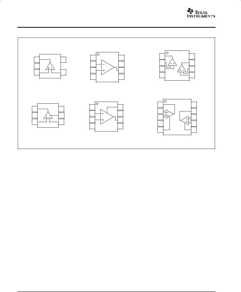
PIN CONFIGURATIONS |
|
|
|
|
|
|
|
|||||
|
|
|
|
|
|
|
OPA735 |
|
|
|
OPA2735 |
|
|
|
OPA735 |
|
|
|
|
|
|
|
|
|
|
|
|
|
|
|
|
|
|
|
|
|
|
|
|
|
|
|
|
NC(1) |
1 |
8 |
NC(1) |
OUT A |
1 |
8 |
V+ |
Out |
|
1 |
|
5 |
|
|
|
|
||||
|
|
V+ |
|
|
|
−IN A |
2 |
7 |
OUT B |
|||
V− |
|
|
|
|
−IN |
2 |
7 |
V+ |
||||
|
2 |
|
|
|
|
|
|
|||||
|
|
|
|
|
|
|
+IN A |
3 |
6 |
−IN B |
||
|
|
|
|
|
+IN |
3 |
6 |
OUT |
||||
+IN |
|
3 |
|
4 |
|
|
|
|
||||
|
|
−IN |
|
|
|
V− |
4 |
5 |
+IN B |
|||
|
|
|
|
|
V− |
4 |
5 |
NC(1) |
||||
|
|
SOT23−5 |
|
|
|
|
|
|
|
|
SO−8, MSOP−8 |
|
|
|
|
|
|
|
|
SO−8 |
|
|
|
|
|
|
|
|
|
|
|
|
|
|
|
|
|
|
|
|
|
|
|
|
|
OPA734 |
|
|
|
OPA2734 |
|
|
|
OPA734 |
|
|
|
|
|
|
|
|
|
|
|
|
|
|
|
|
|
|
|
|
|
|
|
|
|
NSB |
|
|
NC(1) |
1 |
8 |
Enable |
OUT A |
1 |
10 |
V+ |
Out |
1 |
6 |
|
|
|
|
|
|||||
|
|
V+ |
|
|
|
− IN A |
2 |
9 |
OUT B |
|||
|
|
|
|
|
− IN |
2 |
7 |
V+ |
||||
V− |
2 |
|
5 |
|
|
|
|
|
||||
|
|
Enable |
|
|
|
+IN A |
3 |
8 |
− IN B |
|||
|
|
|
|
|
+IN |
3 |
6 |
OUT |
||||
+IN |
3 |
|
4 |
|
|
|
|
|
||||
|
|
−IN |
|
|
|
V− |
4 |
7 |
+IN B |
|||
|
|
|
|
|
V− |
4 |
5 |
NC(1) |
||||
|
|
|
|
|
|
|
|
|
||||
|
|
SOT23−6 (2) |
|
|
|
|
|
|
Enable A |
5 |
6 |
Enable B |
|
|
|
|
|
|
|
SO−8 |
|
|
|
MSOP−10 |
|
|
|
|
|
|
|
|
|
|
|
|
|
|
(1)NC = No Connection
(2)Pin 1 of the SOT23-6 is determined by orienting the package marking as shown in the diagram.
4
OPA734, OPA2734
OPA735, OPA2735
www.ti.com
SBOS282B − DECEMBER 2003 − REVISED FEBRUARY 2005
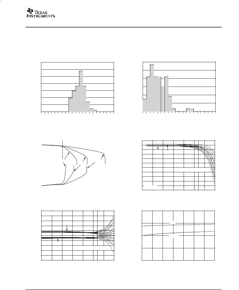
TYPICAL CHARACTERISTICS
At TA = +25°C, VS = ±5V (same as +10V).
OUTPUT VOLTAGE PRODUCTION DISTRIBUTION
Population |
|
|
|
|
|
|
|
|
|
|
|
|
|
|
|
|
|
|
|
|
− 5.0 |
− 4.5 |
− 4.0 |
− 3.5 |
− 3.0 |
− 2.5 |
− 2.0 |
− 1.5 |
− 1.0 |
− 0.5 |
0 |
0.5 |
1.0 |
1.5 |
2.0 |
2.5 |
3.0 |
3.5 |
4.0 |
4.5 |
5.0 |
Offset Voltage (µV)
OUTPUT VOLTAGE SWING TO RAIL vs OUTPUT CURRENT
|
6 |
|
|
|
|
|
|
|
|
|
|
|
|
|
|
|
|
|
|
|
|
|
|
|
|
|
|
|
|
|
|
|
|
|
|
|
|
|
|
(V) |
4 |
|
|
|
|
|
|
|
|
|
|
|
|
|
|
|
|
|
|
|
|
|
+85_C |
|
|
|
|
|
|
−40_C |
|
|
|
||||||
|
|
|
|
|
|
|
|
|
|
|
|
|
|||||||
Swing |
2 |
|
|
|
|
|
|
|
|
|
|
|
|
||||||
|
|
|
|
|
|
|
|
|
|
|
|
|
|
|
|
|
|
|
|
|
|
|
|
|
|
|
|
|
|
|
|
|
|
|
|
|
|
|
|
Voltage |
0 |
|
|
|
|
|
|
|
|
|
+25_C |
|
|
|
|
|
|
|
|
|
|
|
|
|
|
|
|
|
|
|
|
|
|
||||||
OUT |
−2 |
|
|
|
|
|
|
|
|
|
|
|
|
|
|
|
|
|
|
|
|
|
|
|
|
|
|
|
|
|
|
|
|
|
|
|
|
||
|
|
|
|
|
|
|
|
|
|
|
|
|
|
|
|
|
|
|
|
V |
−4 |
|
|
|
|
|
|
|
|
|
|
|
|
|
|
|
|
|
|
|
|
|
|
|
|
|
|
|
|
|
|
|
|
|
|
|
|
|
|
|
|
|
|
|
|
|
|
|
|
|
|
|
|
|
|
|
|
|
|
|
−6 |
|
|
|
|
|
|
|
|
|
|
|
|
|
|
|
|
|
|
|
|
|
|
|
|
|
|
|
|
|
|
|
|
|
|
|
|
|
|
|
0 |
5 |
10 |
15 |
20 |
|
25 |
30 |
35 |
||||||||||
|
|
|
|
|
|
|
Output Current (mA) |
|
|
|
|
|
|
||||||
INPUT BIAS CURRENT vs TEMPERATURE
|
1000 |
|
|
|
|
|
|
|
|
VCM = VS/2 |
|
|
|
|
|
|
|
|
800 |
|
|
|
|
|
|
|
(pA) |
600 |
|
|
+IB |
|
|
|
|
400 |
|
|
|
|
|
|
||
|
|
|
|
|
|
|
||
Current |
200 |
|
|
|
|
|
|
|
0 |
|
|
|
|
|
|
|
|
Bias |
−200 |
−IB |
|
|
|
|
|
|
Input |
−400 |
|
|
|
|
|
|
|
|
|
|
10 Representative Units |
|
||||
−600 |
|
|
|
|
||||
|
|
|
|
|
|
|
|
|
|
−800 |
|
|
|
|
|
|
|
|
−1000 |
|
|
|
|
|
|
|
|
−50 |
− 25 |
0 |
25 |
50 |
75 85 |
100 |
125 |
Temperature (_C)
OUTPUT VOLTAGE DRIFT PRODUCTION DISTRIBUTION
|
|
|
|
|
|
|
Absolute Value; |
|
||
|
|
|
|
|
|
Centered Around Zero |
|
|||
Population |
|
|
|
|
|
|
|
|
|
|
0 |
0.005 |
0.010 |
0.015 |
0.020 |
0.025 |
0.030 |
0.035 |
0.040 |
0.045 |
0.050 |
|
|
|
Offset Voltage Drift (µV/_C) |
|
|
|
||||
INPUT BIAS CURRENT vs TEMPERATURE
|
1000 |
|
|
|
|
|
|
|
|
0 |
|
|
|
|
|
|
|
(pA) |
−1000 |
− IB |
|
+ I |
|
|
|
|
|
|
|
|
|
|
|||
−2000 |
|
|
B |
|
|
|
|
|
|
|
|
|
|
|
|
||
Current |
−3000 |
|
|
|
|
|
|
|
−4000 |
|
|
|
|
|
|
|
|
−5000 |
|
|
|
|
|
|
|
|
Bias |
|
|
|
10 Representative Units |
|
|||
−6000 |
|
|
|
|
||||
|
|
|
|
|
|
|
||
Input |
|
|
|
|
|
|
|
|
−7000 |
|
|
|
|
|
|
|
|
−8000 |
|
|
|
|
|
|
|
|
|
|
|
|
|
|
|
|
|
|
−9000 |
VCM = V− |
|
|
|
|
|
|
|
− 10000 |
|
|
|
|
|
|
|
|
|
|
|
|
|
|
|
|
|
−50 |
− 25 |
0 |
25 |
50 |
75 85 |
100 |
125 |
|
|
|
|
Temperature (_C) |
|
|
|
|
SUPPLY CURRENT vs TEMPERATURE
|
800 |
|
|
|
|
|
|
|
(µA) |
600 |
|
|
± 6V |
|
|
|
|
|
|
|
|
|
|
|
|
|
Supply Current |
400 |
|
|
± 1.35V |
|
|
|
|
200 |
|
|
|
|
|
|
|
|
|
|
|
|
|
|
|
|
|
|
0 |
|
|
|
|
|
|
|
|
−50 |
−25 |
0 |
25 |
50 |
75 |
100 |
125 |
|
|
|
|
Temperature (_C) |
|
|
|
|
5

OPA734, OPA2734
OPA735, OPA2735
SBOS282B − DECEMBER 2003 − REVISED FEBRUARY 2005
TYPICAL CHARACTERISTICS (continued)
At TA = +25°C, VS = ±5V (same as +10V).
OPEN−LOOP GAIN AND PHASE MARGIN vs FREQUENCY
|
180 |
|
|
|
|
|
|
|
|
|
|
|
|
|
|
|
|
|
|
|
|
|
|
|
|
|
|
|
|
|
|
|
|
|
|
|
|
|
|
|
|
|
|
|
|
|
|
|
|
|
|
|
180 |
|
|
|
|
|
|
|
|
|
|
|
|
|
|
|
|
|
|
|
|
|
|
|
|
|
|
|
|
|
|
|
|
|
|
|
|
|
|
|
|
|
|
|
|
|
|
|
|
|
|
|
|
|
|
||
|
160 |
|
|
|
|
|
|
|
|
|
|
|
|
|
|
|
|
|
|
|
|
|
|
|
|
|
|
|
|
|
|
|
|
|
|
|
|
|
|
|
|
|
|
|
|
|
|
|
|
|
|
|
160 |
|
|
|
|
|
|
|
|
|
|
|
|
|
|
|
|
|
|
|
|
|
|
|
|
|
|
|
|
|
|
|
|
|
|
|
|
|
|
|
|
|
|
|
|
|
|
|
|
|
|
|
|
|
|
||
|
140 |
|
|
|
|
|
|
|
|
|
|
|
|
|
|
|
|
|
|
|
|
|
|
|
|
|
|
|
|
|
|
|
|
|
|
|
|
|
|
|
|
|
|
|
|
|
|
|
|
|
|
|
140 |
|
|
|
|
|
|
|
|
|
|
|
|
|
|
|
|
|
|
|
|
|
|
|
|
|
|
|
|
|
|
|
|
|
|
|
|
|
|
|
|
|
|
|
|
|
|
|
|
|
|
|
|
|
|
||
|
120 |
|
|
|
|
|
|
|
|
|
|
|
|
|
|
|
|
|
|
|
|
|
|
|
|
|
|
|
|
|
|
|
|
|
|
|
|
|
|
|
|
|
|
|
|
|
|
|
|
|
|
|
120 |
) |
|
|
|
|
|
|
|
|
|
|
|
|
|
|
|
|
|
|
|
|
|
|
|
|
|
|
|
|
|
|
|
|
|
|
|
|
|
|
|
|
|
|
|
|
|
|
|
|
|
|
|
|
|||
|
100 |
|
|
|
|
|
|
|
|
|
|
|
|
|
|
|
|
|
|
|
|
|
|
|
|
|
|
|
|
|
|
|
|
|
|
|
|
|
|
|
|
|
|
|
|
|
|
|
|
|
|
|
100 |
(_ |
OL |
|
|
|
|
|
|
|
|
|
|
|
|
|
|
|
|
|
|
|
|
|
|
|
|
|
|
|
|
|
|
|
|
|
|
|
|
|
|
|
|
|
|
|
|
|
|
|
|
|
|
|
Margin |
||
60 |
|
|
|
|
|
|
|
|
|
|
|
|
|
|
|
|
|
|
|
|
|
|
|
|
|
|
|
|
|
|
|
|
|
|
|
|
|
|
|
|
|
|
|
|
|
|
|
|
|
|
|
60 |
||
(dB) |
80 |
|
|
|
|
|
|
|
|
|
|
|
|
|
|
|
|
|
|
|
|
|
|
|
|
|
|
|
|
|
|
|
|
|
|
|
|
|
|
|
|
|
|
|
|
|
|
|
|
|
|
|
80 |
|
A |
|
|
|
|
|
|
|
|
|
|
|
|
|
|
|
|
|
|
|
|
|
|
|
|
|
|
|
|
|
|
|
|
|
|
|
|
|
|
|
|
|
|
|
|
|
|
|
|
|
|
|
|
|
Phase |
40 |
|
|
|
|
|
|
|
|
|
|
|
|
|
|
|
|
|
|
|
|
|
|
|
|
|
|
|
|
|
|
|
|
|
|
|
|
|
|
|
|
|
|
|
|
|
|
|
|
|
|
40 |
|||
|
|
|
|
|
|
|
|
|
|
|
|
|
|
|
|
|
|
|
|
|
|
|
|
|
|
|
|
|
|
|
|
|
|
|
|
|
|
|
|
|
|
|
|
|
|
|
|
|
|
|
|
|||
|
20 |
|
|
|
|
|
|
|
|
|
|
|
|
|
|
|
|
|
|
|
|
|
|
|
|
|
|
|
|
|
|
|
|
|
|
|
|
|
|
|
|
|
|
|
|
|
|
|
|
|
|
20 |
|
|
|
|
|
|
|
|
|
|
|
|
|
|
|
|
|
|
|
|
|
|
|
|
|
|
|
|
|
|
|
|
|
|
|
|
|
|
|
|
|
|
|
|
|
|
|
|
|
|
|
|
|
|
|||
|
0 |
|
|
|
|
|
|
|
|
|
|
|
|
|
|
|
|
|
|
|
|
|
|
|
|
|
|
|
|
|
|
|
|
|
|
|
|
|
|
|
|
|
|
|
|
|
|
|
|
|
|
0 |
|
|
|
|
|
|
|
|
|
|
|
|
|
|
|
|
|
|
|
|
|
|
|
|
|
|
|
|
|
|
|
|
|
|
|
|
|
|
|
|
|
|
|
|
|
|
|
|
|
|
|
|
|
|
|||
|
− 20 |
|
|
|
|
|
|
|
|
|
|
|
|
|
|
|
|
|
|
|
|
|
|
|
|
|
|
|
|
|
|
|
|
|
|
|
|
|
|
|
|
|
|
|
|
|
|
|
|
|
|
|
−20 |
|
|
|
|
|
|
|
|
|
|
|
|
|
|
|
|
|
|
|
|
|
|
|
|
|
|
|
|
|
|
|
|
|
|
|
|
|
|
|
|
|
|
|
|
|
|
|
|
|
|
|
|
|
|
||
|
− 40 |
|
|
|
|
|
|
|
|
|
|
|
|
|
|
|
|
|
|
|
|
|
|
|
|
|
|
|
|
|
|
|
|
|
|
|
|
|
|
|
|
|
|
|
|
|
|
|
|
|
−40 |
|
||
|
|
|
|
|
|
|
|
|
|
|
|
|
|
|
|
|
|
|
|
|
|
|
|
|
|
|
|
|
|
|
|
|
|
|
|
|
|
|
|
|
|
|
|
|||||||||||
|
0.1 |
|
|
|
|
|
|
1 |
|
|
10 |
|
|
100 |
|
|
1k |
10k |
100k |
1M |
10M |
|
||||||||||||||||||||||||||||||||
|
|
|
|
|
|
|
|
|
|
|
|
|
|
|
|
|
|
|
|
|
Frequency (Hz) |
|
|
|
|
|
|
|
|
|
|
|
|
|
|
|
|
|
|
|
|
|||||||||||||
|
|
|
|
|
|
|
|
|
|
|
|
|
|
|
SMALL−SIGNAL RESPONSE |
|
|
|
|
|
|
|
|
|
|
|
|
|
|
|||||||||||||||||||||||||
|
|
|
|
|
|
|
|
|
|
|
|
|
|
|
|
|
|
|
|
|
|
|
|
|
|
|
|
|
|
|
|
|
|
|
|
|
|
|
|
|
|
|
|
|
|
|
|
|
||||||
|
Output Voltage (10mV/div) |
|
|
|
|
|
|
|
|
|
|
|
|
|
|
|
|
|
|
|
|
|
|
|
|
|
|
|
|
|
|
|
|
|
|
|
|
|
|
|
|
|
|
|
|
|
|
|
|
|
|
|
|
|
|
|
|
|
|
|
|
|
|
|
|
|
|
|
|
|
|
|
|
|
|
|
|
|
|
|
|
|
|
|
|
|
|
|
|
|
|
|
|
|
|
|
|
|
|
|
|
|
|
|
|
|
|
|
|
|
|
|
|
|
|
|
|
|
|
|
|
|
|
|
|
|
|
|
|
|
|
|
|
|
|
|
|
|
|
|
|
|
|
|
|
|
|
|
|
|
|
|
|
|
|
|
|
|
|
|
|
|
|
|
|
|
|
|
|
|
|
|
|
|
|
|
|
|
|
|
|
|
|
|
|
|
|
|
|
|
|
|
|
|
|
|
|
|
|
|
|
|
|
|
|
|
|
|
|
|
|
|
|
|
|
|
|
|
|
|
|
|
|
|
|
|
|
|
|
|
|
|
|
|
|
|
|
|
|
|
|
|
|
|
|
|
|
|
|
|
|
|
|
|
|
|
|
|
|
|
|
|
|
|
|
|
|
|
|
|
|
|
|
|
|
|
|
|
|
|
|
|
|
|
|
|
|
|
|
|
|
|
|
|
|
|
|
|
|
|
|
|
|
|
|
|
|
|
|
|
|
|
|
|
|
|
|
|
|
|
|
|
|
|
|
|
|
|
|
|
|
|
|
|
|
|
|
|
|
|
|
|
|
|
|
|
|
|
|
|
|
|
|
|
|
|
|
|
|
|
|
|
|
|
|
|
|
|
|
|
|
|
|
|
|
|
|
|
|
|
|
|
|
|
|
|
|
|
|
|
|
|
|
|
|
|
|
|
|
|
|
|
|
|
|
|
|
|
|
|
|
|
|
|
|
|
|
|
|
|
|
|
|
|
|
|
|
|
|
|
|
|
|
|
|
|
|
|
|
|
|
|
|
|
|
|
|
|
|
|
|
|
|
|
|
|
|
|
|
|
|
|
|
|
|
|
|
|
|
|
|
|
|
|
|
|
|
|
|
|
|
|
|
|||||||||||
|
|
|
|
|
|
|
|
|
|
|
|
|
|
|
|
|
|
|
|
|
|
|
|
|
|
|
|
|
|
|
|
|
|
|
|
|
|
|
|
|
|
|
|
|
|
|
|
|
|
|
|
|
|
|
|
|
|
|
|
|
|
|
|
|
|
|
|
|
|
|
|
|
|
|
Time (250ns/div) |
|
|
|
|
|
|
|
|
|
|
|
|
|
|
|
|
|
|
|
|
||||||||||||||
www.ti.com
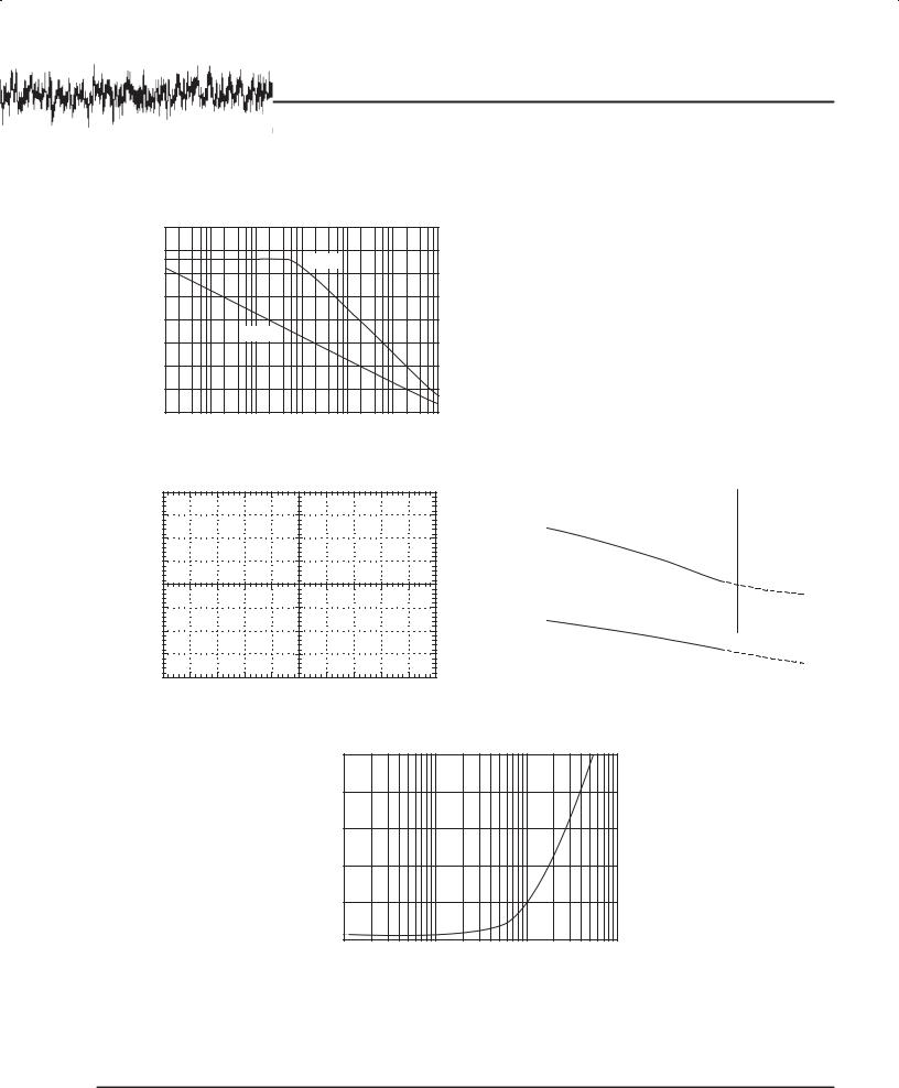
LARGE−SIGNAL RESPONSE
Output Voltage (2V/div)
Time (5µs/div)
POSITIVE OVERVOLTAGE RECOVERY
|
Output |
|
(2V/div) |
|
|
Voltage |
|
+5V |
|
|
10kΩ |
|
10kΩ |
|
|
|
OPA735 |
|
Input |
− 5V |
|
|
|
|
Time (2.5µs/div) |
|
|
NEGATIVE OVERVOLTAGE RECOVERY |
|
||
|
|
|
10kΩ |
|
|
|
10kΩ |
+5V |
|
|
|
|
|
|
Voltage(2V/div) |
|
|
OPA 73 5 |
CMRR(dB) |
Input |
|
Output |
||
|
|
− 5V |
|
|
|
Time (2.5µs/div) |
|
|
|
COMMON−MODE REJECTION RATIO vs FREQUENCY
140
120
100
80
60
40
20
0
1 |
10 |
100 |
1k |
10k |
100k |
1M |
10M |
|
|
|
Frequency (Hz) |
|
|
|
|
6
OPA734, OPA2734
OPA735, OPA2735
www.ti.com
SBOS282B − DECEMBER 2003 − REVISED FEBRUARY 2005
TYPICAL CHARACTERISTICS (continued)
At TA = +25°C, VS = ±5V (same as +10V).
PSRR (dB)
POWER−SUPPLY REJECTION RATIO vs FREQUENCY
160
140
+PSRR
120
100
80
− PSRR
60
40
20
0
1 10 100 1k 10k 100k 1M
Frequency (Hz)
0.1Hz TO 10Hz NOISE
1 V/div
1s/div
VOLTAGE NOISE vs FREQUENCY
|
|
(nV/√Hz) |
1k |
|
|
|
|
|
|
|
|
|
|
|
|
|
|
|
|
|
|
|
|
|
|
|
|
|
|
|
|
|
|
|
|
|
|
|
|
|
|
|
|
|
|
|
|
|
|
|
|
100 |
|
|
|
|
|
|
|
|
|
|
|
|
|
|
|
|
|
|
|
|
|
|
|
|
|
|
|
|
|
|
|
|
|
|
|
|
|
|
|
|
|
|
|
|
|
|
|
|
|
|
|
|
|
|
|
|
|
|
|
|
|
|
|
|
|
|
|
|
|
|
|
|
|
|
|
|
|
|
|
|
|
|
|
|
|
|
|
|
|
|
|
|
|
|
|
||
|
|
|
|
|
|
|
|
|
|
|
|
|
|
|
|
|
|
|
|
|
|
|
|
|
|
|
|
|
|
|
|
|
|
|
|
|
|
|
|
|
|
|
|
|
|
|
|
||
|
|
|
|
|
|
|
|
|
|
|
|
|
|
|
|
|
|
|
|
|
|
|
|
|
|
|
|
|
|
|
|
|
|
|
|
|
|
|
|
|
|
|
|
|
|
|
|
||
|
|
|
|
|
|
|
|
|
|
|
|
|
|
|
|
|
|
|
|
|
|
|
|
|
|
|
|
|
|
|
|
|
|
|
|
|
|
|
|
|
|
|
|
|
|
|
|
||
|
|
|
|
|
|
|
|
|
|
|
|
|
|
|
|
|
|
|
|
|
|
|
|
|
|
|
|
|
|
|
|
|
|
|
|
|
|
|
|
|
|
|
|
|
|
|
|
||
|
|
|
|
|
|
|
|
|
|
|
|
|
|
|
|
|
|
|
|
|
|
|
|
|
|
|
|
|
|
|
|
|
|
|
|
|
|
|
|
|
|
|
|
|
|
|
|||
|
|
|
|
|
|
|
|
|
|
|
|
|
|
|
|
|
|
|
|
|
|
|
|
|
|
|
|
|
|
|
|
|
|
|
|
|
|
|
|
|
|
|
|
|
|
|
|
||
|
|
|
|
|
|
|
|
|
|
|
|
|
|
|
|
|
|
|
|
|
|
|
|
|
|
|
|
|
|
|
|
|
|
|
|
|
|
|
|
|
|
|
|
|
|
|
|
||
|
|
Noise |
10 |
|
|
|
|
|
|
|
|
|
|
|
|
|
|
|
|
|
|
|
|
|
|
|
|
|
|
|
|
|
|
|
|
|
|
|
|
|
|
|
|
|
|
|
|
|
|
|
|
|
|
|
|
|
|
|
|
|
|
|
|
|
|
|
|
|
|
|
|
|
|
|
|
|
|
|
|
|
|
|
|
|
|
|
|
|
|
|
|
|
|
|
|
|
|
||
|
|
|
|
|
|
|
|
|
|
|
|
|
|
|
|
|
|
|
|
|
|
|
|
|
|
|
|
|
|
|
|
|
|
|
|
|
|
|
|
|
|
|
|
|
|
|
|
||
|
|
|
|
|
|
|
|
|
|
|
|
|
|
|
|
|
|
|
|
|
|
|
|
|
|
|
|
|
|
|
|
|
|
|
|
|
|
|
|
|
|
|
|
|
|
|
|
||
|
|
|
|
|
|
|
|
|
|
|
|
|
|
|
|
|
|
|
|
|
|
|
|
|
|
|
|
|
|
|
|
|
|
|
|
|
|
|
|
|
|
|
|
|
|
|
|
|
|
|
|
|
|
|
|
|
|
|
|
|
|
|
|
|
|
|
|
|
|
|
|
|
|
|
|
|
|
|
|
|
|
|
|
|
|
|
|
|
|
|
|
|
|
|
|
|
|
|
|
|
|
|
|
|
|
|
|
|
|
|
|
|
|
|
|
|
|
|
|
|
|
|
|
|
|
|
|
|
|
|
|
|
|
|
|
|
|
|
|
|
|
|
|
|
|
|
|
|
|
|
|
|
|
|
|
|
|
|
|
|
|
|
|
|
|
|
|
|
|
|
|
|
|
|
|
|
|
|
|
|
|
|
|
|
|
|
|
|
|
|
|
|
|
|
|
|
|
|
|
|
|
|
1 |
|
|
|
|
|
10 |
|
100 |
|
|
|
|
|
|
|
|
1k |
|
|
|
|
10k |
|
100k |
||||||||||||||||||||||
|
|
|
|
|
|
|
|
|
|
|
|
|
|
|
|
|
|
Frequency (Hz) |
|
|
|
|
|
|
|
|
|
|
|
|
|
|
|
|
|
|
|||||||||||||
|
|
|
|
|
|
SAMPLING FREQUENCY vs TEMPERATURE |
|
|
|
|
|
||||||||||||||||||||||||||||||||||||||
|
|
|
20.0 |
|
|
|
|
|
|
|
|
|
|
|
|
|
|
|
|
|
|
|
|
|
|
|
|
|
|
|
|
|
|
|
|
|
|
|
|
|
|
|
|
|
|
|
|
|
|
|
|
|
|
|
|
|
|
|
|
|
|
|
|
|
|
|
|
|
|
|
|
|
|
|
|
|
|
|
|
|
|
|
|
|
|
|
|
|
|
|
|
|
|
|
|
|
|
|
|
|
|
(kHz) |
19.5 |
|
|
|
|
|
|
|
|
|
|
|
|
|
|
|
|
|
|
|
|
|
|
|
|
|
|
|
|
|
|
|
|
|
|
|
|
|
|
|
|
|
|
|
|
|
|
|
|
|
|
|
|
|
|
|
|
|
|
|
|
|
|
|
|
|
|
|
|
|
|
|
|
|
|
|
|
|
|
|
|
|
|
|
|
|
|
|
|
|
|
|
|
|
|
||
|
|
19.0 |
|
|
|
|
|
|
|
|
|
|
|
|
|
|
|
|
|
|
|
|
|
|
|
|
|
|
|
|
|
|
|
|
|
|
|
|
|
|
|
|
|
|
|
|
|
|
|
|
|
Frequency |
|
|
|
|
|
|
|
|
|
|
|
|
|
|
|
|
|
|
VS = 12V |
|
|
|
|
|
|
|
|
|
|
|
|
|
|
|
|
|
|
|
|
||||||||
|
|
|
|
|
|
|
|
|
|
|
|
|
|
|
|
|
|
|
|
|
|
|
|
|
|
|
|
|
|
|
|
|
|
|
|
|
|
|
|
|
|||||||||
|
|
18.5 |
|
|
|
|
|
|
|
|
|
|
|
|
|
|
|
|
|
|
|
|
|
|
|
|
|
|
|
|
|
|
|
|
|
|
|
|
|
|
|
|
|
|
|
|
|
|
|
|
|
|
|
|
|
|
|
|
|
|
|
|
|
|
|
|
|
|
|
|
|
|
|
|
|
|
|
|
|
|
|
|
|
|
|
|
|
|
|
|
|
|
|
|
|
|
|
|
|
|
|
Sampling |
18.0 |
|
|
|
|
|
|
|
|
|
|
|
|
|
|
|
|
|
|
|
|
|
|
|
|
|
|
|
|
|
|
|
|
|
|
|
|
|
|
|
|
|
|
|
|
|
|
|
|
|
|
|
|
|
|
|
|
|
|
|
|
|
|
|
|
|
|
|
|
|
|
|
|
|
|
|
|
|
|
|
|
|
|
|
|
|
|
|
|
|
|
|
|
|
|
||
|
|
17.5 |
|
|
|
|
|
|
|
|
|
|
|
|
|
|
|
|
|
|
|
|
|
|
|
|
|
|
|
|
VS = 2.7V |
|
|
|
|
|
|
||||||||||||
|
|
|
|
|
|
|
|
|
|
|
|
|
|
|
|
|
|
|
|
|
|
|
|
|
|
|
|
|
|
|
|
|
|
|
|
|
|
|
|
|
|
|
|
|
|
|
|
|
|
|
|
|
17.0 |
|
|
|
|
|
|
|
|
|
|
|
|
|
|
|
|
|
|
|
|
|
|
|
|
|
|
|
|
|
|
|
|
|
|
|
|
|
|
|
|
|
|
|
|
|
|
|
|
|
|
|
|
|
|
|
|
|
|
|
|
|
|
|
|
|
|
|
|
|
|
|
|
|
|
|
|
|
|
|
|
|
|
|
|
|
|
|
|
|
|
|
|
|
|
|
|
|
|
|
|
|
|
|
|
|
|
|
|
|
|
|
|
|
|
|
|
|
|
|
|
|
|
|
|
|
|
|
|
|
|
|
|
|
|
|
|
|
|
|
|
|
|
|
|
|
|
|
|
|
16.5 |
|
|
|
|
|
|
|
|
|
|
|
|
|
|
|
|
|
|
|
|
|
|
|
|
|
|
|
|
|
|
|
|
|
|
|
|
|
|
|
|
|
|
|
|
|
|
|
|
|
|
|
|
|
|
|
|
|
|
|
|
|
|
|
|
|
|
|
|
|
|
|
|
|
|
|
|
|
|
|
|
|
|
|
|
|
|
|
|
|
|
|
|
|
|
|
|
|
|
|
|
|
|
|
|
|
|
|
|
|
|
|
|
|
|
|
|
|
|
|
|
|
|
|
|
|
|
|
|
|
|
|
|
|
|
|
|
|
|
|
|
|
|
|
|
|
|
|
|
|
16.0 |
|
|
|
|
|
|
|
|
|
|
|
|
|
|
|
|
|
|
|
|
|
|
|
|
|
|
|
|
|
|
|
|
|
|
|
|
|
|
|
|
|
|
|
|
|
|
|
|
|
|
|
|
|
|
|
|
|
|
|
|
|
|
|
|
|
|
|
|
|
|
|
|
|
|
|
|
|
|
|
|
|
|
|
|
|
|
|
|
|
|
|
|
|
|
|
|
|
|
|
−50 |
|
− 25 |
0 |
25 |
50 |
75 |
100 125 |
|
150 |
|||||||||||||||||||||||||||||||||||||
Temperature (_C)
Overshoot (%)
SMALL−SIGNAL OVERSHOOT vs CAPACITIVE LOAD
50
40
30
20
10
0
1 |
10 |
100 |
1000 |
|
Capacitance (pF) |
|
|
7
 Loading...