


 Loading...
Texas Instruments LM3526M, LM3526M-H, LM3526M-L, LM3526MX, LM3526MX-H Schematic [ru]
...LM3526
www.ti.com |
SNVS054E –FEBRUARY 2000–REVISED MARCH 2013 |
LM3526 Dual Port USB Power Switch and Over-Current Protection
Check for Samples: LM3526
FEATURES
•Compatible with USB1.1 and USB 2.0
•1 ms Fault Flag Delay Filters Hot-Plug Events
•Smooth Turn-on Eliminates In-rush Induced Voltage Drop
•UL Recognized Component: REF# 205202
•1A Nominal Short Circuit Output Current Protects PC Power Supplies
•Thermal Shutdown Protects Device in Direct Short Condition
•500mA Minimum Continuous Load Current
•Small SOIC-8 package minimizes board space
•2.7V to 5.5V Input Voltage Range
•140 mΩ Max. Switch Resistance
•1 µ A Max. Standby Current
•200 µ A Max. Operating Current
•Under-voltage Lockout (UVLO)
APPLICATIONS
•Universal Serial Bus (USB) Root Hubs including Desktop and Notebook PC
•USB Monitor Hubs
•Other Self-Powered USB Hub Devices
•High Power USB Devices Requiring In-rush Limiting
•General Purpose High Side Switch Applications
DESCRIPTION
The LM3526 provides Universal Serial Bus standard power switch and over-current protection for all host port applications. The dual port device is ideal for Notebook and desktop PC'sthat supply power to more than one port.
A 1 ms delay on the fault flag output prevents erroneous overcurrent reporting caused by in-rush currents during hot-plug events.
The dual stage thermal protection circuit in the LM3526 provides individual protection to each switch and the entire device. In a short-circuit/over-current event, the switch dissipating excessive heat is turned off, allowing the second switch to continue to function uninterrupted.
The LM3526 accepts an input voltage between 2.7V and 5.5V allowing use as a device-based in-rush current limiter for 3.3V USB peripherals, as well as Root and Self-Powered Hubs at 5.5V. The Enable inputs accept both 3.3V and 5.0V logic thresholds.
The small size, low RON, and 1 ms fault flag delay make the LM3526 a good choice for root hubs as well as per-port power control in embedded and standalone hubs.
Please be aware that an important notice concerning availability, standard warranty, and use in critical applications of
Texas Instruments semiconductor products and disclaimers thereto appears at the end of this data sheet.
All trademarks are the property of their respective owners.
PRODUCTION DATA information is current as of publication date. |
Copyright © 2000–2013, Texas Instruments Incorporated |
Products conform to specifications per the terms of the Texas |
|
Instruments standard warranty. Production processing does not |
|
necessarily include testing of all parameters. |
|
LM3526
SNVS054E –FEBRUARY 2000 –REVISED MARCH 2013 |
www.ti.com |
These devices have limited built-in ESD protection. The leads should be shorted together or the device placed in conductive foam during storage or handling to prevent electrostatic damage to the MOS gates.
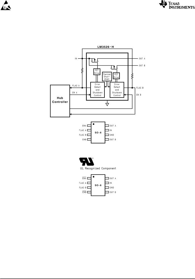
Typical Operating Circuit and Connection Diagram
Figure 1. LM3526-H
Figure 2. LM3526-L
2 |
Submit Documentation Feedback |
Copyright © 2000–2013, Texas Instruments Incorporated |
Product Folder Links: LM3526

|
|
LM3526 |
www.ti.com |
SNVS054E –FEBRUARY 2000–REVISED MARCH 2013 |
|
Absolute Maximum Ratings(1) (2) |
|
|
Supply Voltage |
|
−0.3V to 6V |
Output Voltage |
|
−0.3V to 6V |
Voltage at All Other Pins |
|
−0.3V to 5.5V |
Power Dissipation (T = 25°C)(3) |
|
700 mW |
A |
|
|
(3) |
|
150°C |
TJMAX |
|
|
(1)Absolute Maximum Ratings indicate limits beyond which damage to the device may occur. Electrical specifications do not apply when operating the device beyond its rated operating conditions.
(2)If Military/Aerospace specified devices are required, please contact the Texas Instruments Sales Office/Distributors for availability and specifications.
(3)The maximum power dissipation must be derated at elevated temperatures and is dictated by TJMAX (Maximum junction temperature), θJA (junction to ambient thermal resistance), and TA (ambient temperature). The maximum allowable power dissipation at any temperature is PDMAX = (TJMAX − TA)/θJA or the number given in the Absolute Maximum Ratings, which ever is lower. θJA = 150°C/W.
Operating Ratings
Supply Voltage Range |
2.7V to 5.5V |
|
|
Operating Ambient Range |
−40°C to 85°C |
Operating Junction Temperature Range |
−40°C to 125°C |
Storage Temperature Range |
−65°C to +150°C |
Lead Temperature (Soldering, 5 seconds) |
260°C |
|
|
ESD Rating(1) |
2kV |
ESD Rating Output Only |
8kV |
|
|
(1)The human body model is a 100 pF capacitor discharged through a 1.5 kΩ resistor into each pin. Enable pin ESD threshold is 1.7kV.
DC Electrical Characteristics
Limits in standard typeface are for TJ = 25°C, and limits in boldface type apply over the full operating temperature range. Unless otherwise specified: VIN = 5.0V, VEN = 0V (LM3526-L) or VEN = VIN (LM3526-H).
Symbol |
|
|
Parameter |
|
|
Conditions |
Min |
Typ |
Max |
Units |
||
|
|
|
|
|
|
|
|
|
|
|
|
|
RON |
|
On Resistance |
VIN = 5V, IOUT = 500mA, each switch |
|
100 |
140 |
mΩ |
|||||
|
VIN = 2.7V, IOUT = 500mA, each switch |
|
110 |
180 |
||||||||
|
|
|
|
|
|
|||||||
IOUT |
|
OUT pins continuous output |
Each Output |
0.5 |
|
|
A |
|||||
|
|
current |
|
|
|
|
|
|
|
|
|
|
I |
|
Short Circuit Output Current |
Each Output (enable into Load)(1) |
|
|
|
A |
|||||
SC |
|
|
|
|
|
|
|
|
|
|
|
|
|
|
|
|
VOUT = 4.0V |
0.5 |
1.2 |
1.9 |
|
||||
|
|
|
|
VOUT = 0.1V |
|
1 |
1.5 |
|
||||
OCTHRESH |
|
Over-current Threshold |
|
|
|
|
|
|
2.2 |
3.2 |
A |
|
ILEAK |
|
OUT pins Output Leakage |
V |
|
= VIN (LM3526-L) |
|
0.01 |
10 |
µA |
|||
|
EN |
|
||||||||||
|
|
Current |
VEN = 0V (LM3526-H) |
|
|
|
|
|||||
|
|
|
|
IFO = 10 mA, VIN = 5.0V |
|
10 |
25 |
|
||||
RFO |
|
FLAG Output Resistance |
IFO = 10 mA, VIN = 3.3V |
|
11 |
35 |
Ω |
|||||
|
|
|
|
IFO = 10 mA, VIN = 2.7V |
|
12 |
40 |
|
||||
IEN |
|
|
|
V |
|
/VEN = 0V or V |
|
/VEN = VIN |
−0.5 |
|
0.5 |
µA |
|
EN/EN Leakage Current |
|
|
|
||||||||
|
EN |
EN |
|
|||||||||
V |
|
|
|
See(2) |
2.4 |
1.9 |
|
V |
||||
|
EN/EN Input Logic High |
|
||||||||||
IH |
|
|
|
|
|
|
|
|
|
|
|
|
V |
|
|
|
See(2) |
|
1.7 |
0.8 |
V |
||||
|
EN/EN Input Logic Low |
|
||||||||||
IL |
|
|
|
|
|
|
|
|
|
|
|
|
VUVLO |
|
Under-Voltage Lockout |
|
|
|
|
|
|
1.8 |
|
V |
|
|
|
Threshold |
|
|
|
|
|
|
|
|
|
|
IDDOFF |
|
Supply Current |
Switch-Off |
|
0.2 |
1 |
µA |
|||||
|
|
|
|
−40°C ≤ TJ ≤ 85°C |
|
|
2 |
|
||||
IDDON |
|
Supply Current |
Switch-On |
|
115 |
200 |
µA |
|||||
ThSD |
|
Over-temperature Shutdown |
TJ Increasing, with no shorted output |
|
150 |
|
°C |
|||||
|
|
Threshold |
TJ Increasing, with shorted output (s) |
|
145 |
|
|
|||||
|
|
|
|
T Decreasing(1) |
|
135 |
|
|
||||
|
|
|
|
J |
|
|
|
|
||||
(1)Thermal Shutdown will protect the device from permanent damage.
(2)For LM3526-L, OFF is EN ≥ 2.4V and ON is EN ≤ 0.8V. For LM3526-H, OFF is EN ≤ 0.8V and ON is EN ≥ 2.4V.
Copyright © 2000–2013, Texas Instruments Incorporated |
Submit Documentation Feedback |
3 |
Product Folder Links: LM3526
LM3526
SNVS054E –FEBRUARY 2000 –REVISED MARCH 2013 |
www.ti.com |
DC Electrical Characteristics (continued)
Limits in standard typeface are for TJ = 25°C, and limits in boldface type apply over the full operating temperature range. Unless otherwise specified: VIN = 5.0V, VEN = 0V (LM3526-L) or VEN = VIN (LM3526-H).
Symbol |
Parameter |
|
Conditions |
Min |
Typ |
Max |
Units |
|
|
|
|
|
|
|
|
IFH |
Error Flag Leakage Current |
Vflag = 5V |
|
|
0.01 |
1 |
µA |
AC Electrical Characteristics
Limits in standard typeface are for TJ = 25°C, and limits in boldface type apply over the full operating temperature range. Unless otherwise specified: VIN = 5.0V.
Symbol |
Parameter |
|
Conditions |
Min |
Typ |
Max |
Units |
||
|
|
|
|
|
|
|
|
|
|
tr |
OUT Rise Time |
RL = 10Ω |
|
|
100 |
|
µs |
||
tf |
OUT Fall Time |
RL = 10Ω |
|
|
5 |
|
µs |
||
tON |
Turn on Delay, |
|
to OUT |
RL = 10Ω |
|
|
150 |
|
µs |
EN |
|
|
|
||||||
tOFF |
Turn off Delay, |
|
to OUT |
RL = 10Ω |
|
|
5 |
|
µs |
EN |
|
|
|
||||||
tOC |
Over Current Flag Delay |
RL = 0 |
|
|
1 |
|
ms |
||
|
|
|
|
|
|
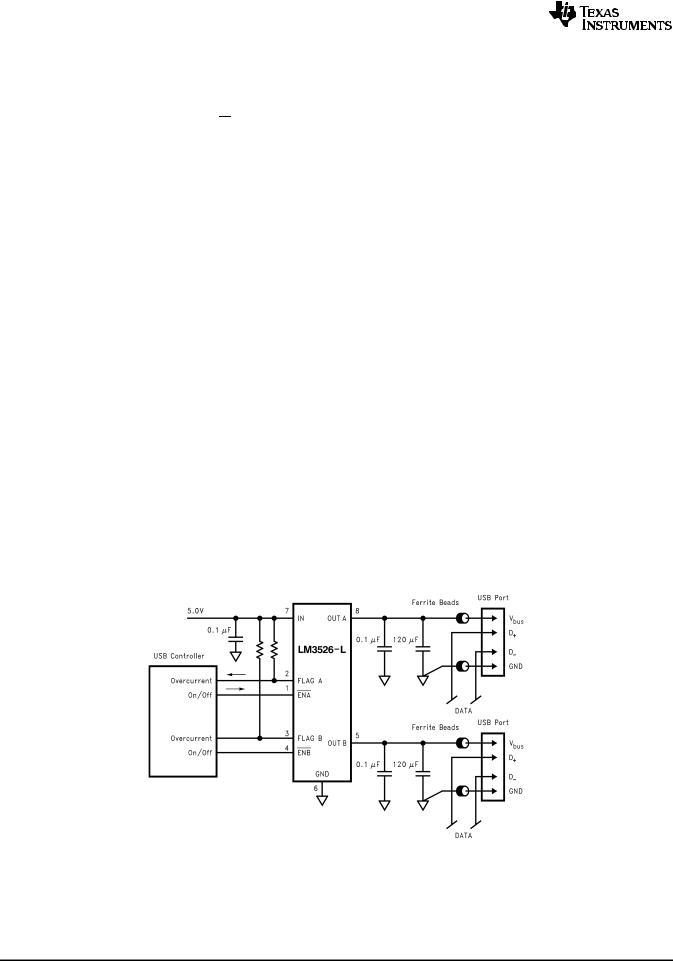
TYPICAL APPLICATION CIRCUIT |
|
|
|
|
|
|
PIN DESCRIPTIONS |
Pin Number |
|
Pin Name |
Pin Function |
|||
|
|
|
|
|
|
|
1, 4 |
|
|
|
|
|
Enable (Input): Logic-compatible enable inputs. |
ENA, |
ENB |
|||||
|
(LM3526-L) |
|
||||
|
|
ENA, ENB |
|
|||
|
(LM3526-H) |
|
||||
|
|
|
|
|
|
|
2, 3 |
|
FLAG A |
Fault Flag (Output): Active-low, open-drain outputs. Indicates overcurrent, UVLO or thermal shutdown. |
|||
|
|
FLAG B |
*See Application Information for more information. |
|||
|
|
|
|
|
|
|
6 |
|
GND |
Ground |
|||
|
|
|
|
|
|
|
7 |
|
IN |
Supply Input: This pin is the input to the power switch and the supply voltage for the IC. |
|||
|
|
|
|
|
|
|
8, 5 |
|
OUT A |
Switch Output: These pins are the outputs of the high side switch. |
|||
|
|
OUT B |
|
|||
|
|
|
|
|
|
|
Figure 3. Typical Application Circuit
4 |
Submit Documentation Feedback |
Copyright © 2000–2013, Texas Instruments Incorporated |
Product Folder Links: LM3526

LM3526
www.ti.com |
SNVS054E –FEBRUARY 2000–REVISED MARCH 2013 |
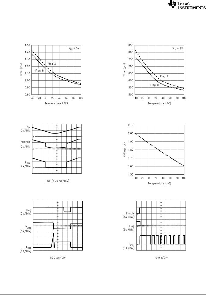
Typical Performance Characteristics
VIN = 5.0V, IL = 500 mA, TA = 25°C unless otherwise specified.
RON |
RON |
vs |
vs |
Temperature |
Temperature |
Figure 4. |
Figure 5. |
Quiescent Current |
Quiescent Current |
vs |
vs |
Input Voltage |
Temperature |
Figure 6. |
Figure 7. |
Current Limit |
OC Threshold |
vs |
vs |
Output Voltage |
Temperature |
Figure 8. |
Figure 9. |
Copyright © 2000–2013, Texas Instruments Incorporated |
Submit Documentation Feedback |
5 |
Product Folder Links: LM3526
LM3526
SNVS054E –FEBRUARY 2000 –REVISED MARCH 2013 |
www.ti.com |
Typical Performance Characteristics (continued)
VIN = 5.0V, IL = 500 mA, TA = 25°C unless otherwise specified.
Fault Flag Delay |
Fault Flag Delay |
vs |
vs |
Temperature |
Temperature |
Figure 10. |
Figure 11. |
|
Under Voltage Lockout Threshold |
|
vs |
Under Voltage Lockout (UVLO) |
Temperature |
Figure 12. |
Figure 13. |
|
Short Circuit Response with |
Over Current/Current Limit Response* |
Thermal Cycling* |
* Output is shorted to Ground through a 100 mΩ resistor |
|
Figure 14. |
Figure 15. |
6 |
Submit Documentation Feedback |
Copyright © 2000–2013, Texas Instruments Incorporated |
Product Folder Links: LM3526
Loading...