Texas Instruments LP339DR, LP339D, LP339N, LP2901N, LP2901DR Datasheet
...
LP239, LP339, LP2901
LOW-POWER QUAD DIFFERENTIAL COMPARATORS
SLCS004A ± OCTOBER 1987 ± REVISED MAY 1988
D Ultralow Power Supply Current |
D, J, OR N PACKAGE |
||||||
|
Drain . . . 60 μA Typ |
|
|
(TOP VIEW) |
|
||
D |
Low Input Biasing Current 3 nA |
1OUT |
|
|
|
|
3OUT |
|
1 |
14 |
|
||||
D Low Input Offset Current . . . ±0.5 nA |
|
|
|||||
2OUT |
|
2 |
13 |
|
4OUT |
||
D Low Input Offset Voltage . . . ±2 mV |
|
|
|||||
VCC |
|
3 |
12 |
|
GND |
||
|
|
||||||
D Common-Mode Input Voltage Includes |
|
|
|||||
2IN ± |
|
4 |
11 |
|
4IN + |
||
|
|
||||||
|
Ground |
2IN + |
|
5 |
10 |
|
4IN ± |
|
|
|
|||||
D Output Voltage Compatible With MOS and |
1IN ± |
|
6 |
9 |
|
3IN + |
|
|
|
||||||
|
CMOS Logic |
1IN + |
|
7 |
8 |
|
3IN ± |
|
|
|
|||||
D High Output Sink-Current Capability |
|
|
|
|
|
|
|
|
|
|
|
|
|
||
|
(30 mA at VO = 2V) |
|
|
|
|
|
|
D |
Power Supply Input Reverse-Voltage |
|
|
|
|
|
|
|
Protected |
|
|
|
|
|
|
D D
Single-Power-Supply Operation
Pin-for-Pin Compatible With LM239, LM339,
LM2901
description
The LP239, LP339, LP2901 are low-power quadruple differential comparators. Each device consists of four independent voltage comparators designed specifically to operate from a single power supply and typically to draw 60-μA drain current over a wide range of voltages. Operation from split power supplies is also possible and the ultralow power supply drain current is independent of the power supply voltage.
Applications include limit comparators, simple analog-to-digital converters, pulse generators, squarewave generators, time delay generators, voltage controlled oscillators, multivibrators, and high-voltage logic gates. The LP239, LP339, LP2901 were specifically designed to interface with the CMOS logic family. The ultralow power supply current makes these products desirable in battery-powered applications.
The LP239 is characterized for operation from ± 25°C to 85°C. The LP339 is characterized for operation from 0°C to 70°C. The LP2901 is characterized for operation from ± 40°C to 85°C.
AVAILABLE OPTIONS
|
|
|
PACKAGE |
|
TA |
VIOmax AT 25°C |
|
|
|
SMALL OUTLINE |
PLASTIC DIP |
CERAMIC DIP |
||
|
|
(D) |
(N) |
(J) |
|
|
|
|
|
0 °C to 70 °C |
± 5 mV |
LP339D |
LP339N |
LP339J |
|
|
|
|
|
± 25 °C to 85 °C |
± 5 mV |
LP239D |
LP239N |
LP239J |
|
|
|
|
|
± 40 °C to 85 °C |
± 5 mV |
LP2901D |
LP2901N |
LP2901J |
|
|
|
|
|
The D package is available taped-and-reeled. Add R suffix to device type when ordering (e.g., LP339DR).
PRODUCTION DATA information is current as of publication date. Products conform to specifications per the terms of Texas Instruments standard warranty. Production processing does not necessarily include testing of all parameters.
Copyright 1988, Texas Instruments Incorporated
POST OFFICE BOX 655303 •DALLAS, TEXAS 75265 |
1 |

LP239, LP339, LP2901
LOW-POWER QUAD DIFFERENTIAL COMPARATORS
SLCS004A ± OCTOBER 1987 ± REVISED MAY 1988
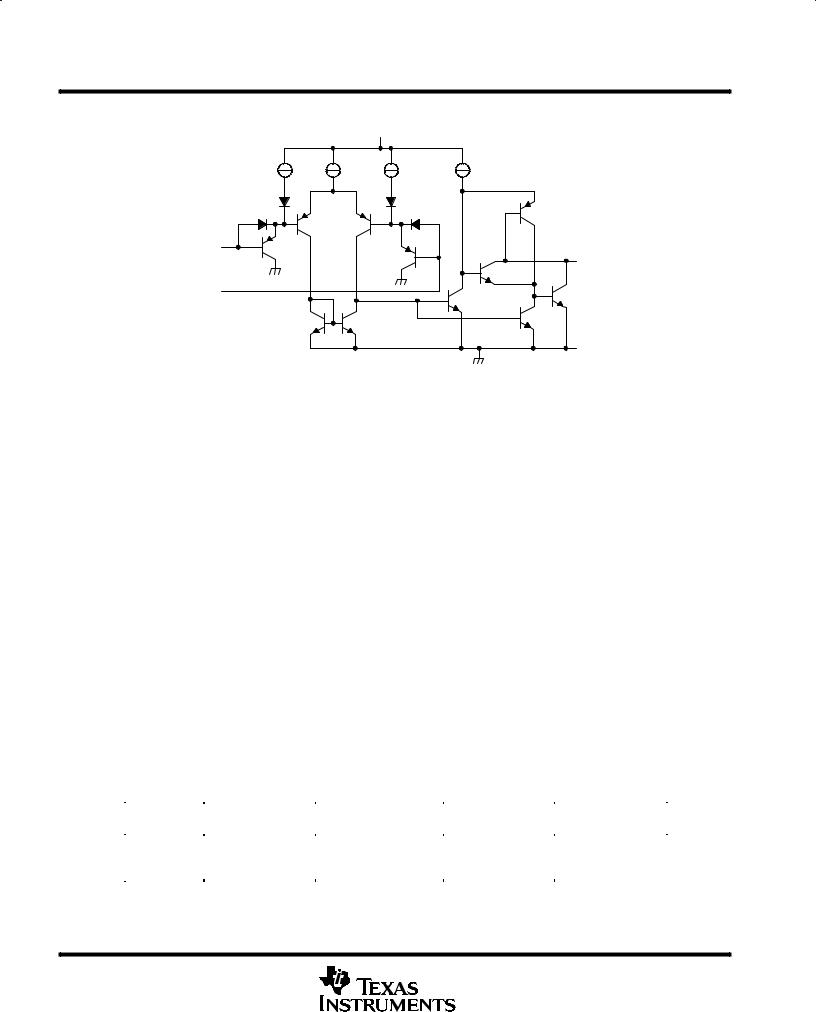
schematic diagram (each comparator)
VCC
0.2 μA |
μA |
0.2 μA |
6 μA |
5 |
IN +
OUT
IN ±
GND
absolute maximum ratings over operating free-air temperature range (unless otherwise noted)²
Supply voltage, VCC (see Note 1) . . . . . . . . . . . . . . . . . . . . . . . . . . . . . . . . . . . . . . . . . . . . . . . . . . . . . . . . . . . . 36 V Differential input voltage, VID (see Note 2) . . . . . . . . . . . . . . . . . . . . . . . . . . . . . . . . . . . . . . . . . . . . . . . . . . . ±36 V Input voltage range, VI (either input) . . . . . . . . . . . . . . . . . . . . . . . . . . . . . . . . . . . . . . . . . . . . . . . . . ± 0.3 V to 36 V Input current, VI ≤ ± 0.3 V (see Note 3) . . . . . . . . . . . . . . . . . . . . . . . . . . . . . . . . . . . . . . . . . . . . . . . . . . . . ± 50 mA Duration of output short-circuit to ground (see Note 4) . . . . . . . . . . . . . . . . . . . . . . . . . . . . . . . . . . . . . . Unlimited
Continuous total dissipation (see Note 5) . . . . . . . . . . . . . . . . . . . . . . . . . . . . . . . . See Dissipation Rating Table
Operating free-air temperature range, TA: LP239 . . . . . . . . . . . . . . . . . . . . . . . . . . . . . . . . . . . . . . ± 25°C to 85°C LP339 . . . . . . . . . . . . . . . . . . . . . . . . . . . . . . . . . . . . . . . . 0°C to 70°C
LP2901 . . . . . . . . . . . . . . . . . . . . . . . . . . . . . . . . . . . . . ± 40°C to 85°C Storage temperature range . . . . . . . . . . . . . . . . . . . . . . . . . . . . . . . . . . . . . . . . . . . . . . . . . . . . . . . ± 65°C to 150°C Lead temperature range 1,6 mm (1/16 inch) from case for 10 seconds: D or N package . . . . . . . . . . . 260°C Lead temperature range 1,6 mm (1/16 inch) from case for 60 seconds: J package . . . . . . . . . . . . . . . . 300°C
²Stresses beyond those listed under absolute maximum ratings may cause permanent damage to the device. These are stress ratings only, and functional operation of the device at these or any other conditions beyond those indicated in the recommended operating conditions is not implied.
Exposure to absolute-maximum-rated conditions for extended periods may affect device reliability.
NOTES: 1. All voltage values, except differential voltages, are with respect to the network ground.
2.Differential voltages are at IN+ with respect to IN ±.
3.This input current only exists when the voltage at any of the inputs is driven negative. The current flows through the collector-base junction of the input clamping device. In addition to the clamping device action, there is lateral n-p-n parasitic transistor action. This
action is not destructive and normal output states are re-established when the input voltage returns to a value more positive than
± 0.3 V at TA = 25°C.
4.Short circuits between outputs to VCC can cause excessive heating and eventual destruction.
5.If the output transistors are allowed to saturate, the low bias dissipation and the on-off characteristics of the outputs keep the dissipation very small (usually less than 100 mW).
DISSIPATION RATING TABLE
PACKAGE |
TA ≤ 25°C |
DERATING FACTOR |
TA = 70°C |
TA = 85°C |
||
POWER RATING |
ABOVE TA = 25°C |
POWER RATING |
POWER RATING |
|||
|
||||||
D |
950 |
mW |
7.6 mW/°C |
608 mW |
494 mW |
|
J |
1025 |
mW |
8.2 mW/°C |
656 mW |
533 mW |
|
N |
1150 |
mW |
9.2 mW/°C |
736 mW |
598 mW |
|
|
|
|
|
|
|
|
2 |
POST OFFICE BOX 655303 •DALLAS, TEXAS 75265 |

LP239, LP339, LP2901
LOW-POWER QUAD DIFFERENTIAL COMPARATORS
SLCS004A ± OCTOBER 1987 ± REVISED MAY 1988
recommended operating conditions
|
|
|
LP239 |
LP339 |
LP2901 |
UNIT |
||||
|
|
|
|
|
|
|
|
|
||
|
|
|
MIN |
MAX |
MIN |
MAX |
MIN |
MAX |
||
|
|
|
|
|||||||
|
|
|
|
|
|
|
|
|
|
|
VCC |
Supply voltage |
5 |
30 |
5 |
30 |
5 |
30 |
V |
||
VIC |
Common-mode input voltage |
VCC = 5 V |
0 |
3 |
0 |
3 |
0 |
3 |
V |
|
VCC = 30 V |
0 |
28 |
0 |
28 |
0 |
28 |
V |
|||
|
|
|||||||||
VI |
Input voltage |
VCC = 5 V |
0 |
3 |
0 |
3 |
0 |
3 |
V |
|
VCC = 30 V |
0 |
28 |
0 |
28 |
0 |
28 |
V |
|||
|
|
|||||||||
TA |
Operating free-air temperature |
± 25 |
85 |
0 |
70 |
± 40 |
85 |
°C |
||
electrical characteristics, VCC = 5 V, TA = 25°C (unless otherwise noted)
|
PARAMETER |
|
TEST CONDITIONS |
T ² |
MIN |
TYP |
MAX |
UNIT |
||
|
|
|
|
|
|
A |
|
|
|
|
VIO |
Input offset voltage |
VCC = 5 V to 30 V, |
VO = 2 V, |
25°C |
|
±2 |
±5 |
mV |
||
|
|
|
|
|||||||
RS = 0, |
See Note 6 |
Full range |
|
|
± |
|||||
|
|
|
|
|
|
|
|
9 |
|
|
IIO |
Input offset current |
|
|
|
|
25°C |
|
±0.5 |
±5 |
nA |
|
|
|
|
|
|
|
|
|||
|
|
|
|
Full range |
|
±1 |
±15 |
|||
|
|
|
|
|
|
|
|
|||
|
|
|
|
|
|
|
|
|
|
|
IIB |
Input bias current |
See Note 7 |
|
25°C |
|
± 2.5 |
± 25 |
nA |
||
|
|
|
|
|
||||||
|
Full range |
|
± 4 |
± 40 |
||||||
|
|
|
|
|
|
|
|
|||
|
|
|
|
|
|
|
|
|
|
|
|
|
|
|
|
|
25°C |
0 to |
|
|
|
|
Common-mode input voltage |
|
|
|
|
VCC ± 1.5 |
|
|
|
|
VICR |
Single supply |
|
|
|
|
V |
||||
range |
|
Full range |
0 to |
|
|
|||||
|
|
|
|
|
|
|
|
|||
|
|
|
|
|
|
VCC ± 2 |
|
|
|
|
|
|
|
|
|
|
|
|
|
|
|
AVD |
Large-signal differential voltage |
VCC = 15 V, |
RL = 15 kΩ |
|
|
500 |
|
V/mV |
||
amplification |
|
|
|
|||||||
|
|
|
|
|
|
|
|
|
|
|
|
|
|
|
|
|
|
|
|
|
|
|
|
VI ± = 1 V, |
|
VO = 2 V, |
25°C |
20 |
30 |
|
|
|
|
|
|
|
|
|
|
|
|||
|
Output sink current |
|
See Note 8 |
Full range |
15 |
|
|
mA |
||
|
|
VI + = 0 |
|
|
|
|
|
|
|
|
|
|
|
VO = 0.4 V |
25°C |
0.2 |
0.7 |
|
|
||
|
|
|
|
|
|
|
||||
|
|
V |
= 1 V, |
|
VO = 5 V |
25°C |
|
0.1 |
|
nA |
|
Output leakage current |
I + |
|
|
|
|
|
|
|
|
|
VI ± = 0 |
|
VO = 30 V |
Full range |
|
|
1 |
μA |
||
|
|
|
|
|
||||||
VID |
Differential input voltage |
VI ≤ 0 (or VCC ± on split supplies) |
|
|
|
36 |
V |
|||
ICC |
Supply current |
RL = ∞ all comparators |
|
|
|
60 |
100 |
μA |
||
² Full range is ±25°C to 85°C for the LP239, 0°C to 70°C for the LP339, and ± 40°C to 85°C for the LP2901. |
|
|
|
|||||||
NOTES: 6. VIO is measured over the full common-mode input voltage range. |
|
|
|
|
|
|||||
7.Because of the p-n-p input stage, the direction of the current is out of the device. This current is essentially constant (i.e., independent of the output state). No loading change exists on the reference or input lines as long as the common-mode input voltage range is not exceeded.
8.The output sink current is a function of the output voltage. These devices have a bimodal output section that allows them to sink
(via a Darlington connection) large currents at output voltages greater than 1.5 V, and smaller currents at output voltages less than 1.5 V.
switching characteristics, VCC = 5 V, TA = 25°C, RL connected to 5 V through 5.1 kΩ
PARAMETER |
TEST CONDITIONS |
MIN |
TYP MAX |
UNIT |
|
|
|
|
|
Large-signal response time |
TTL logic swing, Vref = 1.4 V |
|
1.3 |
μs |
|
|
|
||
Response time |
|
8 |
||
|
|
|
||
|
|
|
|
|
POST OFFICE BOX 655303 •DALLAS, TEXAS 75265 |
3 |
 Loading...