


LM3671LC
Table of contents
 Loading...
Texas Instruments LM3671LC, LM3671LC-1.2, LM3671LC-1.3, LM3671LC-1.6, LM3671LC-1.8 Schematic [ru]
...
1
2
5
43
V
IN
SW
FB
EN
GND
L1: 2.2 PH
V
OUT
C
OUT
10 PF
C
IN
4.7 PF
LM3671
V
IN
2.7V to 5.5V
www.ti.com
SNVS294P –NOVEMBER 2004–REVISED MAY 2013
LM3671, LM3671Q 2MHz, 600mA Step-Down DC-DC Converter
Check for Samples: LM3671, LM3671Q
1
FEATURES
2
• 16 µA Typical Quiescent Current
• 600 mA Maximum Load Capability • PDAs
• 2 MHz PWM Fixed Switching Frequency (typ.) • MP3 Players
• Automatic PFM/PWM Mode Switching • W-LAN
• Internal Synchronous Rectification for High • Portable Instruments
Efficiency
• Internal Soft start
• 0.01 µA Typical Shutdown Current
• Operates from a Single Li-Ion Cell Battery
• Only Three Tiny Surface-Mount External
Components Required (One Inductor, Two
Ceramic Capacitors)
• Current Overload and Thermal Shutdown
Protection
• Available in Fixed Output Voltages and
Adjustable Version
• LM3671Q is an Automotive Grade Product that
is AEC-Q100 Grade 1 Qualified
• SOT-23, 5-Bump DSBGA and 6-Pin USON
Packages
APPLICATIONS
• Mobile Phones
• Digital Still Cameras
• Portable Hard Disk Drives
• Automotive
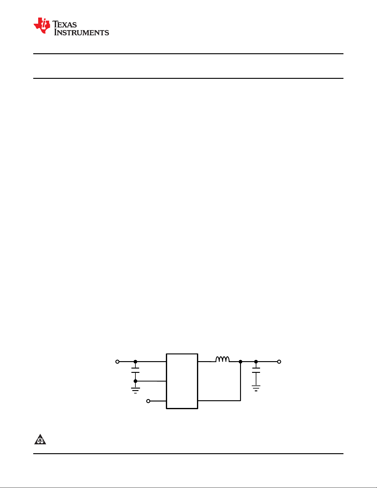
DESCRIPTION
The LM3671 step-down DC-DC converter is
optimized for powering low voltage circuits from a
single Li-Ion cell battery and input voltage rails from
2.7V to 5.5V. It provides up to 600 mA load current,
over the entire input voltage range. There are several
different fixed voltage output options available as well
as an adjustable output voltage version range from
1.1V to 3.3V.
The device offers superior features and performance
for mobile phones and similar portable systems.
Automatic intelligent switching between PWM lownoise and PFM low-current mode offers improved
system control. During PWM mode, the device
operates at a fixed-frequency of 2 MHz (typ.).
Hysteretic PFM mode extends the battery life by
reducing the quiescent current to 16 µA (typ.) during
light load and standby operation. Internal
synchronous rectification provides high efficiency
during PWM mode operation. In shutdown mode, the
device turns off and reduces battery consumption to
0.01 µA (typ.).
LM3671
LM3671Q
TYPICAL APPLICATION CIRCUITS
Figure 1. Typical Application Circuit
1
2All trademarks are the property of their respective owners.
PRODUCTION DATA information is current as of publication date.
Products conform to specifications per the terms of the Texas
Instruments standard warranty. Production processing does not
necessarily include testing of all parameters.
Please be aware that an important notice concerning availability, standard warranty, and use in critical applications of
Texas Instruments semiconductor products and disclaimers thereto appears at the end of this data sheet.
Copyright © 2004–2013, Texas Instruments Incorporated
A3
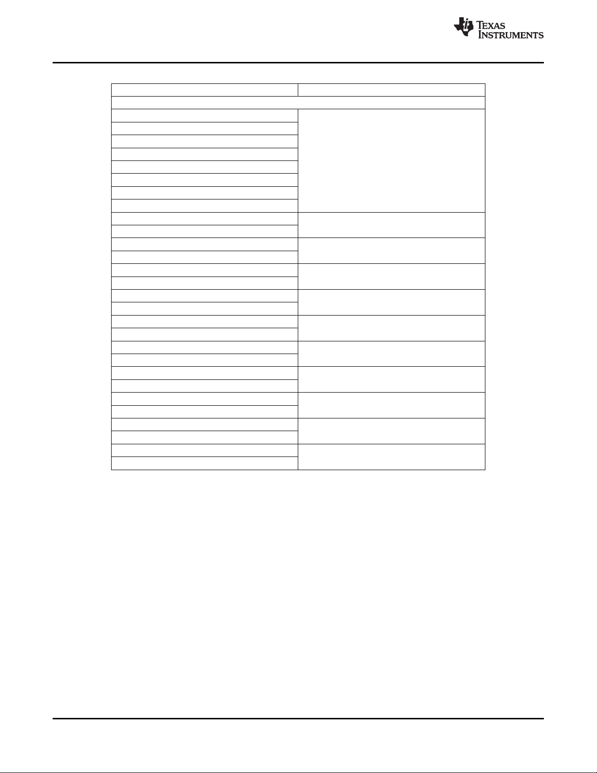
Top View Bottom View
A1
C1
A3
C3
EN
FB
SW
GND
V
IN
EN
GND
SW
FB
B2
V
IN
A1
C3
C1
B2
V
IN
1
GND2EN
3
FB
4
SW
5
1
2
5
43
V
IN
SW
FB
EN
GND
L1: 2.2 PH
V
OUT
C
OUT
10 PF
C
IN
4.7 PF
LM3671-
ADJ
V
IN
2.7V to 5.5V
R1
R2
C1
C2
LM3671
LM3671Q
SNVS294P –NOVEMBER 2004–REVISED MAY 2013
DESCRIPTION (CONTINUED)
The LM3671 is available in SOT-23, tiny 5-bump DSBGA and a 6-pin USON packages in leaded (PB) and leadfree (NO PB) versions. A high-switching frequency of 2 MHz (typ.) allows use of tiny surface-mount components.
Only three external surface-mount components, an inductor and two ceramic capacitors, are required.
Figure 2. Typical Application Circuit for ADJ version
Connection Diagrams
www.ti.com
Figure 3. Top View
SOT-23 Package
See Package Number DBV (2.92 mm x 2.84 mm x 1.2 mm)
Figure 4. 5-Bump DSBGA Package
See Package Number YZR0005 (1.05 mm x 1.38 mm x 0.6 mm)
2 Submit Documentation Feedback Copyright © 2004–2013, Texas Instruments Incorporated
Product Folder Links: LM3671 LM3671Q

1
3 4
6
En
Pgnd
Vin
2
5
Sw
Sgnd
Fb
TOP VIEW
www.ti.com
Pin # Name Description
LM3671
LM3671Q
SNVS294P –NOVEMBER 2004–REVISED MAY 2013
Figure 5. 6-Pin USON Package
See Package Number NKH0006B (2 mm x 2 mm x 0.6 mm)
PIN DESCRIPTIONS (SOT-23)
1 V
IN
2 GND Ground pin.
3 EN Enable pin. The device is in shutdown mode when voltage to this pin is <0.4V and enabled
4 FB Feedback analog input. Connect directly to the output filter capacitor for fixed voltage
5 SW Switching node connection to the internal PFET switch and NFET synchronous rectifier.
Power supply input. Connect to the input filter capacitor (Figure 1).
when >1.0V. Do not leave this pin floating.
versions. For adjustable version external resistor dividers are required (Figure 2). The
internal resistor dividers are disabled for the adjustable version.
PIN DESCRIPTIONS (5-Bump DSBGA)
Pin # Name Description
A1 V
IN
Power supply input. Connect to the input filter capacitor (Figure 1).
A3 GND Ground pin.
C1 EN Enable pin. The device is in shutdown mode when voltage to this pin is <0.4V and enabled
when >1.0V. Do not leave this pin floating.
C3 FB Feedback analog input. Connect directly to the output filter capacitor for fixed voltage
versions. For adjustable version external resistor dividers are required (Figure 2). The
internal resistor dividers are disabled for the adjustable version.
B2 SW Switching node connection to the internal PFET switch and NFET synchronous rectifier.
PIN DESCRIPTIONS (6-Pin USON)
Pin # Name Description
1 EN Enable pin. The device is in shutdown mode when voltage to this pin is <0.4V and enabled
2 Pgnd Ground pin.
3 V
IN
4 SW Switching node connection to the internal PFET switch and NFET synchronous rectifier.
5 Sgnd Singnal ground (feedback ground).
6 FB Feedback analog input. Connect directly to the output filter capacitor for fixed voltage
These devices have limited built-in ESD protection. The leads should be shorted together or the device placed in conductive foam
during storage or handling to prevent electrostatic damage to the MOS gates.
when >1.0V. Do not leave this pin floating.
Power supply input. Connect to the input filter capacitor (Figure 1).
versions. For adjustable version external resistor dividers are required (Figure 2). The
internal resistor dividers are disabled for the adjustable version.
Copyright © 2004–2013, Texas Instruments Incorporated Submit Documentation Feedback 3
Product Folder Links: LM3671 LM3671Q
LM3671
LM3671Q
SNVS294P –NOVEMBER 2004–REVISED MAY 2013
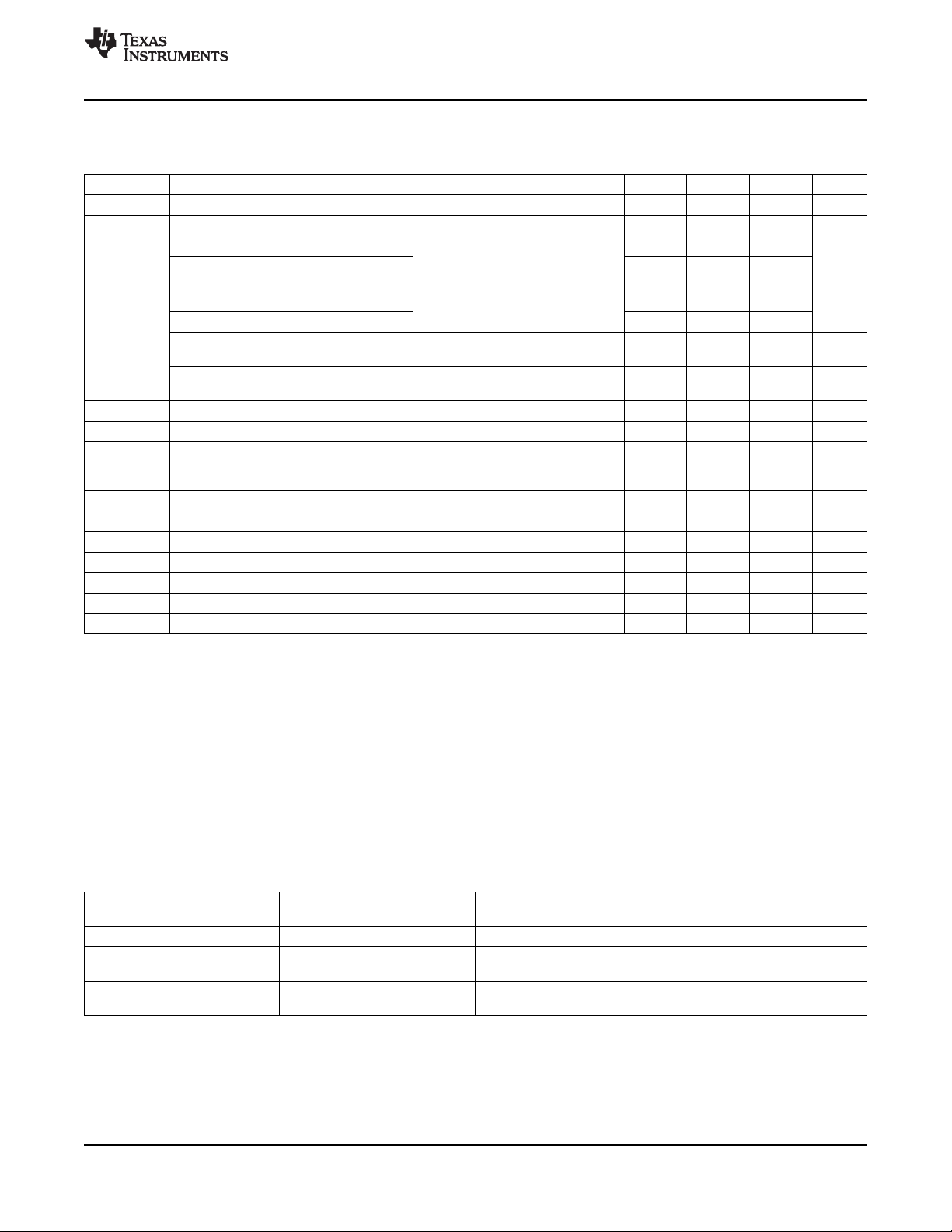
Orderable Voltage Option (V)
SOT-23 Package
LM3671MF-1.2
LM3671MFX-1.2
LM3671MF-1.2/NOPB
LM3671MFX-1.2/NOPB
LM3671QMF-1.2
LM3671QMFX-1.2
LM3671QMF-1.2/NOPB
LM3671QMFX-1.2/NOPB
LM3671MF-1.25/NOPB
LM3671MFX-1.25/NOPB
LM3671MF-1.375/NOPB
LM3671MFX-1.375/NOPB
LM3671MF-1.5/NOPB
LM3671MFX-1.5/NOPB
LM3671MF-1.6/NOPB
LM3671MFX-1.6/NOPB
LM3671MF-1.8/NOPB
LM3671MFX-1.8/NOPB
LM3671MF-1.875/NOPB
LM3671MFX-1.875/NOPB
LM3671MF-2.5/NOPB
LM3671MFX-2.5/NOPB
LM3671MF-2.8/NOPB
LM3671MFX-2.8/NOPB
LM3671MF-3.3/NOPB
LM3671MFX-3.3/NOPB
LM3671MF-ADJ/NOPB
LM3671MFX-ADJ/NOPB
(1) For the most current package and ordering information, see the Package Option Addendum at the end
of this document, or see the TI web site at www.ti.com.
(2) Package drawings, thermal data, and symbolization are available at www.ti.com/packaging.
ORDERING INFORMATION
www.ti.com
(1)(2)
1.2
1.25
1.375
1.5
1.6
1.8
1.875
2.5
2.8
3.3
Adjustable
4 Submit Documentation Feedback Copyright © 2004–2013, Texas Instruments Incorporated
Product Folder Links: LM3671 LM3671Q

www.ti.com
DSBGA Package
LM3671TL-1.2/NOPB
LM3671TLX-1.2/NOPB
LM3671TL-1.25/NOPB
LM3671TLX-1.25/NOPB
LM3671TL-1.5/NOPB
LM3671TLX-1.5/NOPB
LM3671TL-1.8/NOPB
LM3671TLX-1.8/NOPB
LM3671TL-1.875/NOPB
LM3671TLX-1.875/NOPB
LM3671TL-2.5/NOPB
LM3671TLX-2.5/NOPB
LM3671TL-2.8/NOPB
LM3671TLX-2.8/NOPB
LM3671TL-3.3/NOPB
LM3671TLX-3.3/NOPB
LM3671TL-ADJ/NOPB
LM3671TLX-ADJ/NOPB
USON Package
LM3671LC-1.2/NOPB
LM3671LCX-1.2/NOPB
LM3671LC-1.3/NOPB
LM3671LCX-1.3/NOPB
LM3671LC-1.6/NOPB
LM3671LCX-1.6/NOPB
LM3671LC-1.8/NOPB
LM3671LCX-1.8/NOPB
SNVS294P –NOVEMBER 2004–REVISED MAY 2013
ORDERING INFORMATION
Orderable Voltage Option (V)
(1)(2)
(continued)
1.2
1.25
1.5
1.8
1.875
2.5
2.8
3.3
Adjustable
1.2
1.3
1.6
1.8
LM3671
LM3671Q
Copyright © 2004–2013, Texas Instruments Incorporated Submit Documentation Feedback 5
Product Folder Links: LM3671 LM3671Q
LM3671
LM3671Q
SNVS294P –NOVEMBER 2004–REVISED MAY 2013
ABSOLUTE MAXIMUM RATINGS
(1)(2)
VINPin: Voltage to GND −0.2V to 6.0V
FB, SW, EN Pin: (GND−0.2V) to
Continuous Power Dissipation
Junction Temperature (T
(3)
) +125°C
J-MAX
Storage Temperature Range −65°C to +150°C
Maximum Lead Temperature 260°C
(Soldering, 10 sec.)
ESD Rating
(4)
Human Body Model 2 kV
Machine Model 200V
(1) Absolute Maximum Ratings indicate limits beyond which damage to the device may occur. Operating Ratings are conditions under
which operation of the device is specified. Operating Ratings do not imply specified performance limits. For specified performance limits
and associated test conditions, see the Electrical Characteristics tables.
(2) If Military/Aerospace specified devices are required, please contact the Texas Instruments Sales Office / Distributors for
availability and specifications.
(3) Internal thermal shutdown circuitry protects the device from permanent damage. Thermal shutdown engages at TJ= 150°C (typ.) and
disengages at TJ= 130°C (typ.).
(4) The Human body model is a 100 pF capacitor discharged through a 1.5 kΩ resistor into each pin. The machine model is a 200 pF
capacitor discharged directly into each pin. MIL-STD-883 3015.7
www.ti.com
(VIN+ 0.2V)
Internally Limited
OPERATING RATINGS
Input Voltage Range
(3)
(1) (2)
2.7V to 5.5V
Recommended Load Current 0mA to 600 mA
Junction Temperature (TJ) Range −40°C to +125°C
Ambient Temperature (TA) Range
(4)
−40°C to +85°C
(1) Absolute Maximum Ratings indicate limits beyond which damage to the device may occur. Operating Ratings are conditions under
which operation of the device is specified. Operating Ratings do not imply specified performance limits. For specified performance limits
and associated test conditions, see the Electrical Characteristics tables.
(2) All voltages are with respect to the potential at the GND pin.
(3) The input voltage range recommended for ideal applications performance for the specified output voltages are given below:VIN= 2.7V to
4.5V for 1.1V ≤ V
V
DROPOUT
(4) In Applications where high power dissipation and/or poor package resistance is present, the maximum ambient temperature may have
= I
to be derated. Maximum ambient temperature (T
maximum power dissipation of the device in the application (P
in the application, as given by the following equation:T
different ambient temperatures.
< 1.5VVIN= 2.7V to 5.5V for 1.5V ≤ V
OUT
LOAD
*( R
DSON, PFET
+ R
INDUCTOR
< 1.8VVIN= (V
)
A-MAX
OUT
) is dependent on the maximum operating junction temperature (T
) and the junction to ambient thermal resistance of the package (θJA)
D-MAX
= T
A-MAX
J-MAX
− (θJAx P
+ V
OUT
). Refer to Dissipation rating table for P
D-MAX
DROPOUT
) to 5.5V for 1.8V ≤ V
≤ 3.3Vwhere
OUT
J-MAX
D-MAX
), the
values at
THERMAL PROPERTIES
Junction-to-Ambient Thermal Resistance (θJA) (SOT-23) for 4-layer board
Junction-to-Ambient Thermal Resistance (θJA) (DSBGA) for 4-layer board
Junction-to-Ambient Thermal Resistance (θJA) (USON) for 4-layer board
(1) Junction to ambient thermal resistance is highly application and board layout dependent. In applications where high power dissipation
exists, special care must be given to thermal dissipation issues in board design. Specified value of 130 °C/W for SOT-23 is based on a 4
layer, 4" x 3", 2/1/1/2 oz. Cu board as per JEDEC standards is used.
(1)
(1)
(1)
130°C/W
85°C/W
165°C/W
6 Submit Documentation Feedback Copyright © 2004–2013, Texas Instruments Incorporated
Product Folder Links: LM3671 LM3671Q
LM3671
LM3671Q
www.ti.com
ELECTRICAL CHARACTERISTICS
(1)(2)(3)
Limits in standard typeface are for TJ= 25°C. Limits in boldface type apply over the entire junction temperature range for
operation, −40°C to +125°C. Unless otherwise noted, specifications apply to the LM3671MF/TL/LC with VIN= EN = 3.6V
Symbol Parameter Condition Min Typ Max Units
V
IN
Input Voltage
Feedback Voltage (Fixed) MF −4 +4
Feedback Voltage (Fixed) TL PWM mode
Feedback Voltage (Fixed) LC −4 +4
Feedback Voltage (ADJ) MF
V
FB
(6)
Feedback Voltage (ADJ) TL −2.5 +2.5
Line Regulation 0.031 %/V
Load Regulation 0.0013 %/mA
V
REF
I
SHDN
I
Q
R
DSON (P)
R
DSON (N)
I
LIM
V
IH
V
IL
I
EN
F
OSC
Internal Reference Voltage 0.5 V
Shutdown Supply Current EN = 0V 0.01 1 µA
DC Bias Current into V
IN
Pin-Pin Resistance for PFET VIN= VGS= 3.6V 380 500 mΩ
Pin-Pin Resistance for NFET VIN= VGS= 3.6V 250 400 mΩ
Switch Peak Current Limit Open Loop
Logic High Input 1.0 V
Logic Low Input 0.4 V
Enable (EN) Input Current 0.01 1 µA
Internal Oscillator Frequency PWM Mode
(1) All voltages are with respect to the potential at the GND pin.
(2) Min and Max limits are specified by design, test or statistical analysis. Typical numbers are not specified, but do represent the most
likely norm.
(3) The parameters in the electrical characteristic table are tested at VIN= 3.6V unless otherwise specified. For performance over the input
voltage range refer to datasheet curves.
(4) The input voltage range recommended for ideal applications performance for the specified output voltages are given below:VIN= 2.7V to
4.5V for 1.1V ≤ V
V
DROPOUT
(5) Test condition: for V
= I
(6) ADJ version is configured to 1.5V output. For ADJ output version: VIN= 2.7V to 4.5V for 0.90V ≤ V
≤ V
< 3.3V
OUT
(7) Refer to datasheet curves for closed loop data and its variation with regards to supply voltage and temperature. Electrical Characteristic
< 1.5VVIN= 2.7V to 5.5V for 1.5V ≤ V
OUT
LOAD
*( R
DSON, PFET
less than 2.5V, VIN= 3.6V; for V
OUT
+ R
INDUCTOR
)
table reflects open loop data (FB=0V and current drawn from SW pin ramped up until cycle by cycle current limit is activated). Closed
loop current limit is the peak inductor current measured in the application circuit by increasing output current until output voltage drops
by 10%.
(4)
(5)
PWM mode
(5)
2.7V ≤ VIN≤ 5.5V
IO= 10 mA
100 mA ≤ IO≤ 600 mA
VIN= 3.6V
No load, device is not switching (FB
forced higher than programmed 16 35 µA
output voltage)
(7)
(5)
< 1.8VVIN= (V
OUT
greater than or equal to 2.5V, VIN= V
OUT
OUT
SNVS294P –NOVEMBER 2004–REVISED MAY 2013
2.7 5.5 V
−2.5 +2.5 %
−4 +4
830 1020 1150 mA
1.6 2 2.6 MHz
+ V
DROPOUT
) to 5.5V for 1.8V ≤ V
+ 1V.
OUT
< 1.1VVIN= 2.7V to 5.5V for 1.1V
OUT
≤ 3.3Vwhere
OUT
%
DISSIPATION RATING TABLE
θ
JA
130°C/W (4 layer board) SOT-23 770 mW 500 mW 310 mW
85°C/W (4 layer board) 5-bump 1179 mW 765 mW 470 mW
DSBGA
165°C/W (4 layer board) 6-pin 606 mW 394 mW 242 mW
USON
Copyright © 2004–2013, Texas Instruments Incorporated Submit Documentation Feedback 7
TA≤ 25°C TA= 60°C TA= 85°C
Power Rating Power Rating Power Rating
Product Folder Links: LM3671 LM3671Q
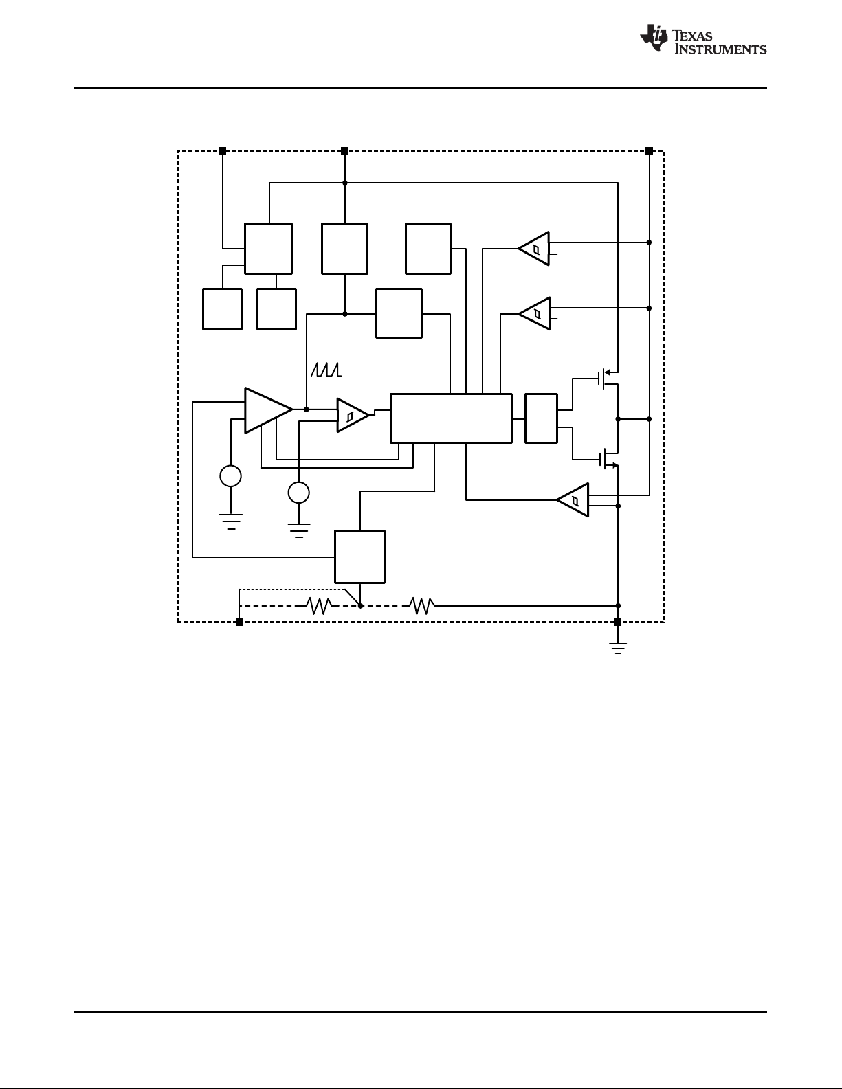
2 MHz
Oscillator
Soft
Start
Ramp
Generator
Thermal
Shutdown
Undervoltage
Lockout
Frequency
Compensation
+
-
Error
Amp
Control Logic Driver
Current Limit
Comparator
Ref1
PFM Current
Comparator
Ref2
SW
Zero Crossing
Comparator
FB
EN
V
IN
PWM Comparator
pfm_low
pfm_hi
GND
Bandgap
+
-
Vcomp
1.0V
Fixed Ver
Adj Ver
+
-
0.5V
+
-
+
-
+
-
V
REF
LM3671
LM3671Q
SNVS294P –NOVEMBER 2004–REVISED MAY 2013
BLOCK DIAGRAM
www.ti.com
8 Submit Documentation Feedback Copyright © 2004–2013, Texas Instruments Incorporated
Figure 6. Simplified Functional Diagram
Product Folder Links: LM3671 LM3671Q
-10 10 30 50 70 90 110
TEMPERATURE (oC)
100
150
200
250
300
350
400
450
500
550
600
R
DS(ON)
(m:)
-30
NFET
VIN = 4.5V
PFET
VIN = 2.7V
VIN = 4.5V
VIN = 3.6V
VIN = 3.6V
VIN = 2.7V
3.0 3.5 4.0 4.5 5.0 5.5 6.0
SUPPLY VOLTAGE (V)
10
12
14
16
18
20
QUIESCENT CURRENT (P
A
)
2.5
TA = 85°C
EN = V
IN
I
OUT
= 0 mA
TA = 25°C
TA = -30°C
-10 10 30 50 70 90
TEMPERATURE (°C)
0.00
0.05
0.10
0.15
0.20
0.25
0.30
0.35
0.40
SHUTDOWN CURRENT (PA)
-30
EN = GND
VIN = 3.6V
VIN = 2.7V
VIN = 5.5V
www.ti.com
SNVS294P –NOVEMBER 2004–REVISED MAY 2013
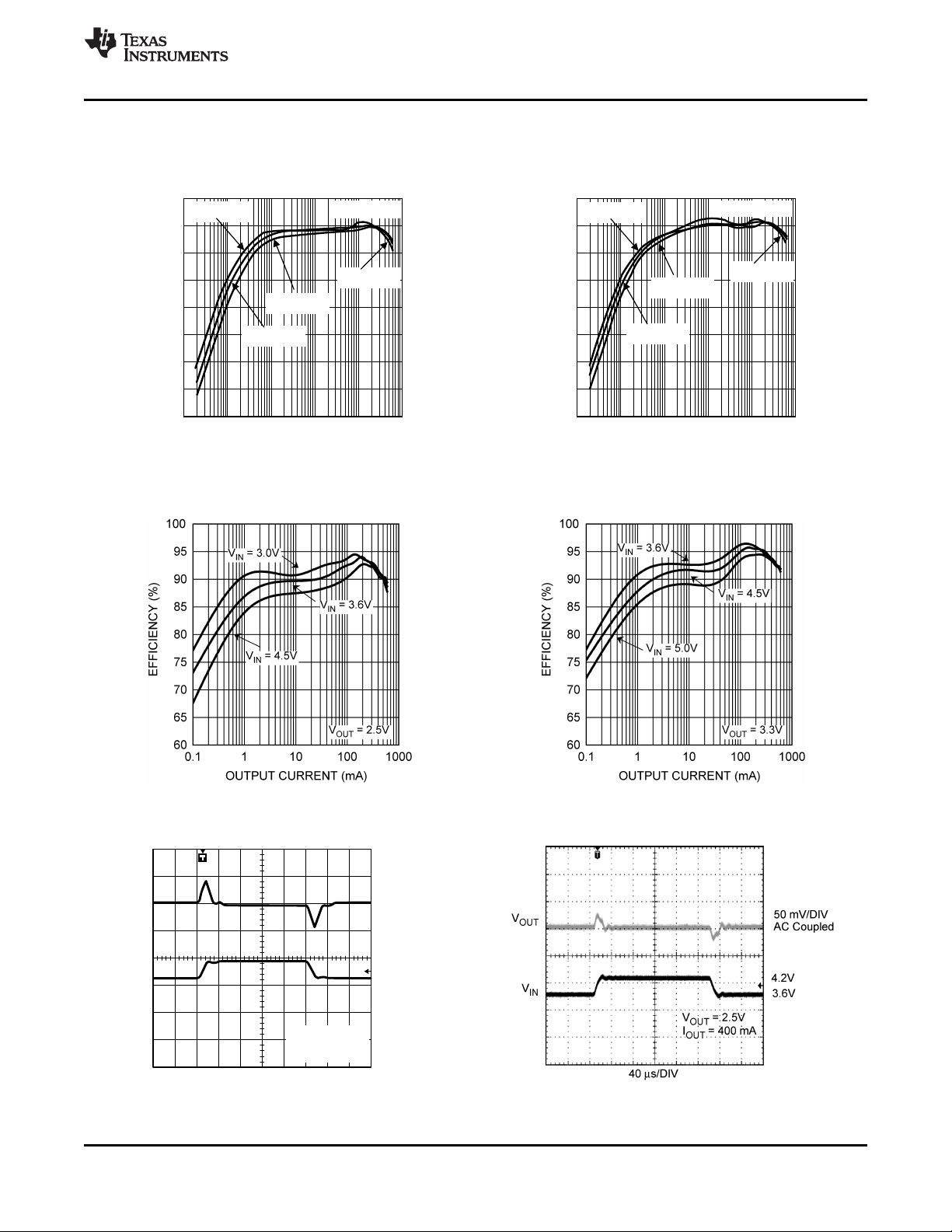
TYPICAL PERFORMANCE CHARACTERISTICS
LM3671MF/TL/LC, Circuit of Figure 1, VIN= 3.6V, V
Quiescent Supply Current vs. Supply Voltage Shutdown Current vs. Temp
Figure 7. Figure 8.
Feedback Bias Current vs. Temp Switching Frequency vs. Temperature
= 1.5V, TA= 25°C, unless otherwise noted.
OUT
LM3671
LM3671Q
Figure 9. Figure 10.
R
vs. Temperature Open/Closed Loop Current Limit vs. Temperature
DS(ON)
Copyright © 2004–2013, Texas Instruments Incorporated Submit Documentation Feedback 9
Figure 11. Figure 12.
Product Folder Links: LM3671 LM3671Q
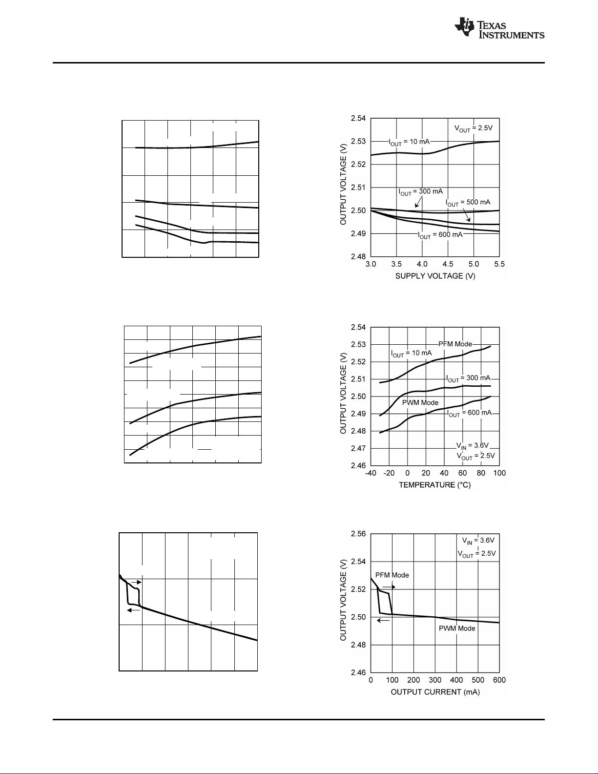
0 100 200 300 400 500 600
OUTPUT CURRENT (mA)
1.48
1.5
1.52
1.54
OUTPUT VOLTAGE (V)
VIN = 3.6V
V
OUT
= 1.5V
PFM Mode
PWM Mode
-10 10 30 50 70 90
TEMPERATURE (oC)
1.4800
1.4850
1.4900
1.4950
1.5000
1.5050
1.5100
1.5150
1.5200
1.5250
1.5300
OUTPUT VOLTAGE (V)
-30
PFM Mode
PWM Mode
I
OUT
= 300 mA
VIN = 3.6V
V
OUT
= 1.5V
I
OUT
= 600 mA
I
OUT
= 10 mA
2.5 3 3.5 4 4.5 5 5.5
SUPPLY VOLTAGE(V)
1.4800
1.4900
1.5000
1.5100
1.5200
1.5300
= 10 mAI
OUT
= 1.5 V
OUT
V
= 300 mA
I
OUT
= 500 mA
I
OUT
= 600 mA
I
OUT
OUTPUT VOLTAGE (V)
LM3671
LM3671Q
SNVS294P –NOVEMBER 2004–REVISED MAY 2013
TYPICAL PERFORMANCE CHARACTERISTICS (continued)
LM3671MF/TL/LC, Circuit of Figure 1, VIN= 3.6V, V
Output Voltage vs. Supply Voltage Output Voltage vs. Supply Voltage
(V
= 1.5V) (V
OUT
Figure 13. Figure 14.
= 1.5V, TA= 25°C, unless otherwise noted.
OUT
OUT
www.ti.com
= 2.5V)
Output Voltage vs. Temperature Output Voltage vs. Temperature
(V
= 1.5V) (V
OUT
OUT
= 2.5V)
Figure 15. Figure 16.
Output Voltage vs. Output Current Output Voltage vs. Output Current
(V
= 1.5V) (V
OUT
OUT
= 2.5V)
10 Submit Documentation Feedback Copyright © 2004–2013, Texas Instruments Incorporated
Figure 17. Figure 18.
Product Folder Links: LM3671 LM3671Q
V
OUT
40 Ps/DIV
3.6V
V
IN
3.0V
20 mV/DIV
AC Coupled
V
OUT
= 1.5V
I
OUT
= 400 mA
0.10 1.00 10.00 100.00 1000.00
OUTPUT CURRENT (mA)
20
30
40
50
60
70
80
90
100
EFFICIENCY (%)
0.01
VIN = 2.7V
VIN = 2.7V
VIN = 4.5V
VIN = 3.6V
V
OUT
= 1.5V
0.10 1.00 10.00 100.00 1000.00
OUTPUT CURRENT (mA)
20
30
40
50
60
70
80
90
100
EFFICIENCY (%)
0.01
VIN = 3.0V
VIN = 3.0V
VIN = 4.5V
VIN = 3.6V
V
OUT
= 1.8V
www.ti.com
TYPICAL PERFORMANCE CHARACTERISTICS (continued)
LM3671MF/TL/LC, Circuit of Figure 1, VIN= 3.6V, V
Efficiency vs. Output Current Efficiency vs. Output Current
(V
= 1.5V, L= 2.2 µH) (V
OUT
Figure 19. Figure 20.
Efficiency vs. Output Current Efficiency vs. Output Current
(V
= 2.5V, L= 2.2 µH) (V
OUT
SNVS294P –NOVEMBER 2004–REVISED MAY 2013
= 1.5V, TA= 25°C, unless otherwise noted.
OUT
OUT
OUT
LM3671
LM3671Q
= 1.8V, L= 2.2 µH)
= 3.3V, L= 2.2 µH)
Figure 21. Figure 22.
Line Transient Response Line Transient Response
V
= 1.5V (PWM Mode) V
OUT
Figure 23. Figure 24.
Product Folder Links: LM3671 LM3671Q
Copyright © 2004–2013, Texas Instruments Incorporated Submit Documentation Feedback 11
= 2.5V (PWM Mode)
OUT
LM3671
LM3671Q
SNVS294P –NOVEMBER 2004–REVISED MAY 2013
TYPICAL PERFORMANCE CHARACTERISTICS (continued)
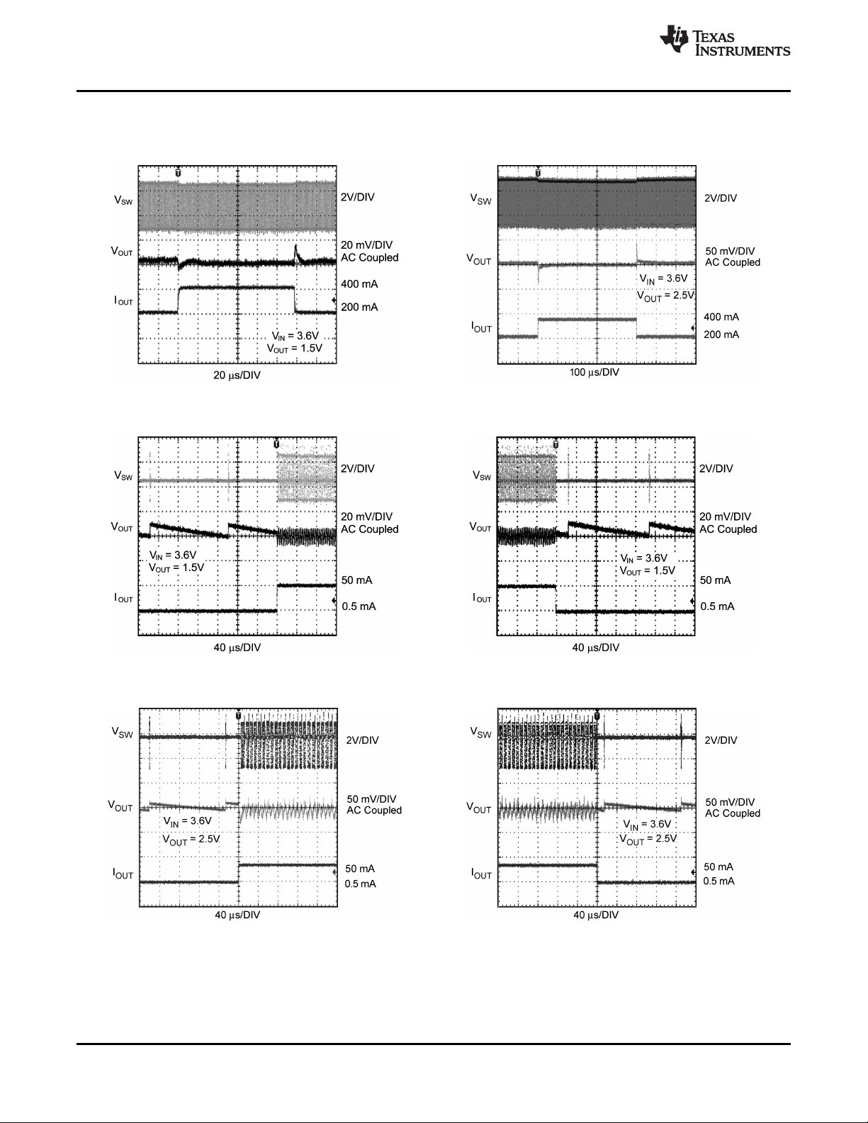
LM3671MF/TL/LC, Circuit of Figure 1, VIN= 3.6V, V
Load Transient Response Load Transient Response
V
= 1.5V (PWM Mode) V
OUT
Figure 25. Figure 26.
= 1.5V, TA= 25°C, unless otherwise noted.
OUT
OUT
www.ti.com
= 2.5V (PWM Mode)
Load Transient Response (V
(PFM Mode 0.5 mA to 50 mA) (PFM Mode 50 mA to 0.5 mA)
Figure 27. Figure 28.
Load Transient Response (V
(PFM Mode 0.5 mA to 50 mA) (PFM Mode 50 mA to 0.5 mA)
= 1.5V) Load Transient Response (V
OUT
= 2.5V) Load Transient Response (V
OUT
OUT
OUT
= 1.5V)
= 2.5V)
Figure 29. Figure 30.
12 Submit Documentation Feedback Copyright © 2004–2013, Texas Instruments Incorporated
Product Folder Links: LM3671 LM3671Q
Loading...