


MSP430P315IDLR
MSP430x31x
MIXED SIGNAL MICROCONTROLLERS
SLAS165D – FEBRUARY 1998 – REVISED APRIL 2000
1
POST OFFICE BOX 655303 • DALLAS, TEXAS 75265
D
Low Supply Voltage Range 2.5 V – 5.5 V
D
Ultra Low-Power Consumption
D
Low Operation Current, 400 µA at 1 MHz,
3V
D
Five Power Saving Modes: (Standby Mode:
1.3 µA, RAM Retention/Off Mode: 0.1 µA)
D
Wakeup From Standby Mode in 6 µs
Maximum
D
16-Bit RISC Architecture, 300 ns Instruction
Cycle Time
D
Single Common 32 kHz Crystal, Internal
System Clock up to 3.3 MHz
D
Integrated LCD Driver for up to 64 or 92
Segments
D
Slope A/D Converter With External
Components
D
Serial Onboard Programming
D
Program Code Protection by Security Fuse
D
Family Members Include:
MSP430C31 1S: 2k Byte ROM,128 Byte RAM
MSP430C312: 4k Byte ROM, 256 Byte RAM
MSP430C313: 8k Byte ROM, 256 Byte RAM
MSP430C314: 12k Byte ROM, 512 Byte RAM
MSP430C315: 16k Byte ROM, 512 Byte RAM
MSP430P313: 8k Byte OTP, 256 Byte RAM
†
MSP430P315: 16k Byte OTP, 512 Byte RAM
MSP430P315S: 16k Byte OTP, 512 ByteRAM
D
EPROM Version Available for Prototyping :
PMS430E313FZ
†
, PMS430E315FZ
D
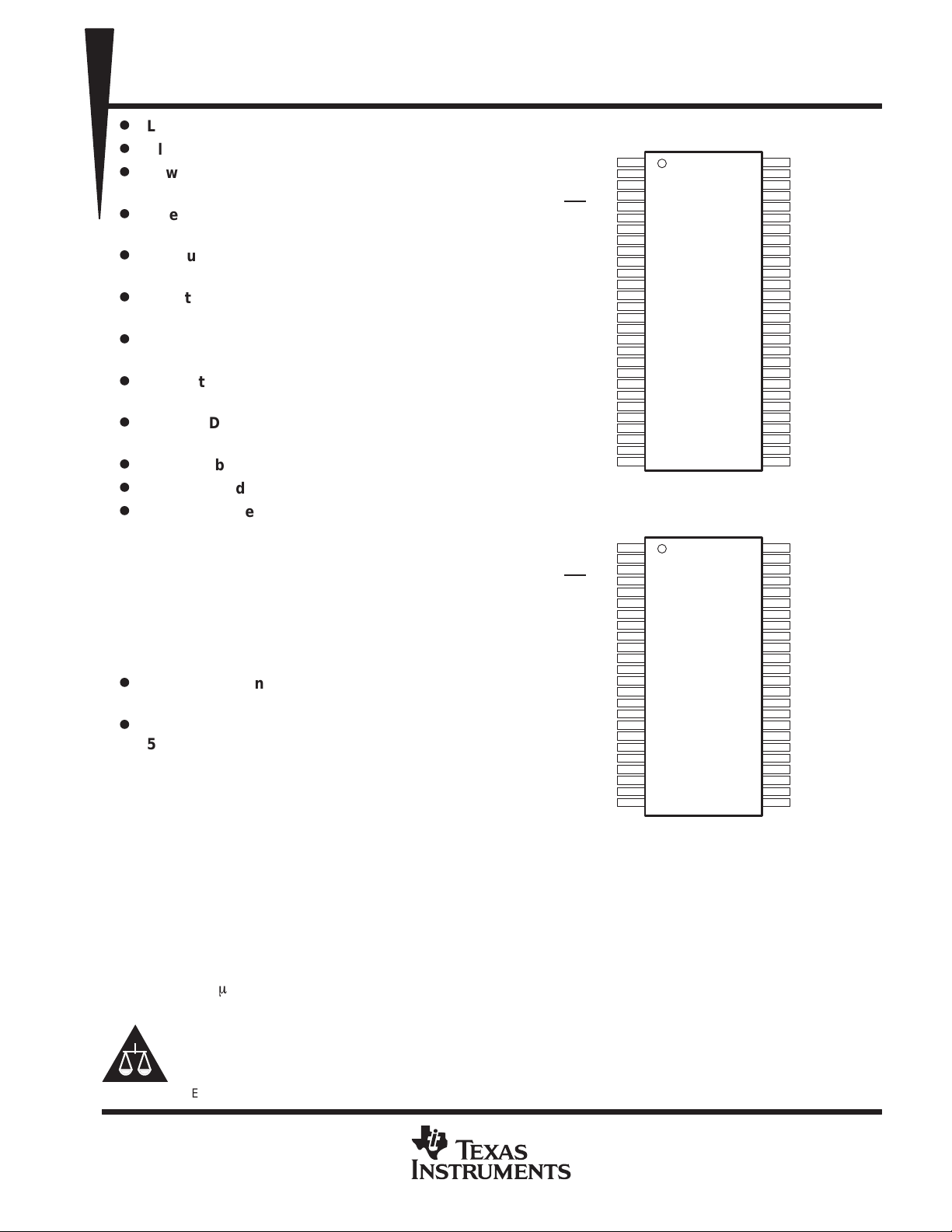
Available in:
56-Pin Plastic Small-Outline Package
(SSOP),
48-Pin SSOP (MSP430C311S,
MSP430P315S),
68-Pin J-Leaded Ceramic Chip Carrier
(JLCC) Package (EPROM Only)
description
The MSP430 is an ultralow-power mixed signal microcontroller family consisting of several devices that feature
different sets of modules targeted to various applications. The microcontroller is designed to be battery operated
for an extended application lifetime. With 16-bit RISC architecture, 16-bit integrated registers on the CPU, and
a constant generator, the MSP430 achieves maximum code efficiency. The digitally-controlled oscillator,
together with the frequency-locked-loop (FLL), provides a wakeup from a low-power mode to active mode in
less than 6
m
s.
†
MSP430P313/E313 not recommended for new designs – replaced by MSP430P315/E315.
Please be aware that an important notice concerning availability, standard warranty, and use in critical applications of
Texas Instruments semiconductor products and disclaimers thereto appears at the end of this data sheet.
Copyright 2000, Texas Instruments Incorporated
PRODUCTION DATA information is current as of publication date.
Products conform to specifications per the terms of Texas Instruments
standard warranty. Production processing does not necessarily include
testing of all parameters.
NC – No internal connection
1
2
3
4
5
6
7
8
9
10
11
12
13
14
15
16
17
18
19
20
21
22
23
24
25
26
27
28
56
55
54
53
52
51
50
49
48
47
46
45
44
43
42
41
40
39
38
37
36
35
34
33
32
31
30
29
TDO/TDI
TDI/VPP
TMS
TCK
RST
/NMI
XBUF
V
SS
V
CC
R23
R13
Xin
Xout/TCLK
P0.0
P0.1/RXD
P0.2/TXD
P0.3
P0.4
P0.5
P0.6
P0.7
TP0.0
TP0.1
TP0.2
TP0.3
TP0.4
TP0.5
CIN
NC
NC
COM3
COM2
COM1
COM0
S27/O27/CMPI
S26/O26
S23/O23
S22/O22
S18/O18
S17/O17
S16/O16
S15/O15
S14/O14
S13/O13
S12/O12
S11/O11
S10/O10
S9/O9
S8/O8
S7/O7
S6/O6
S5/O5
S4/O4
S3/O3
S2/O2
S1
S0
DL PACKAGE
(56-PIN TOP VIEW)
1
2
3
4
5
6
7
8
9
10
11
12
13
14
15
16
17
18
19
20
21
22
23
24
48
47
46
45
44
43
42
41
40
39
38
37
36
35
34
33
32
31
30
29
28
27
26
25
TDI/VPP
TMS
TCK
RST
/NMI
XBUF
V
SS
V
CC
R23
R13
Xin
Xout/TCLK
P0.1/RXD
P0.2/TXD
P0.3
P0.4
P0.5
P0.6
NC
TP0.0
TP0.1
TP0.2
TP0.3
TP0.5
CIN
TDO/TDI
COM3
COM2
COM1
COM0
S27/O27/CMPI
NC
V
SS
NC
S16/O16
S15/O15
S14/O14
S13/O13
S12/O12
S11/O11
S10/O10
S9/O9
S8/O8
S7/O7
S6/O6
S5/O5
S4/O4
S3/O3
S2/O2
DL PACKAGE
(48-PIN TOP VIEW)
MSP430x31x
MIXED SIGNAL MICROCONTROLLERS
SLAS165D – FEBRUARY 1998 – REVISED APRIL 2000
2
POST OFFICE BOX 655303 • DALLAS, TEXAS 75265
description (continued)
Typical applications include sensor systems that capture analog signals, converting them to digital values, and
then processes the data and displays them or transmits them to a host system. The timer/port module provides
single-slope A/D conversion capability for resistive sensors.
AVAILABLE OPTIONS
PACKAGED DEVICES
T
A
SSOP
48-Pin
(DL)
SSOP
56-Pin
(DL)
JLCC
68-Pin
(FZ)
°
°
MSP430C311SIDL
MSP430C312IDL
MSP430C313IDL
MSP430C314IDL
–
40°C
to
85°C
MSP430P315SIDL
MSP430C315IDL
MSP430P313IDL
†
MSP430P315IDL
°
PMS430E313FZ
†
25°C
— —
PMS430E315FZ
†
MSP430P313/E313 not recommended for new designs – replaced by MSP430P315/E315.
functional block diagram
MSP430C312,313,314,315 and MSP430P313
†
,315 and PMS430E313,315
Oscillator
FLL
System Clock
ACLK
MCLK
4/8/12/16 kB
ROM
8/16 kB
C: ROM
256/512 B
RAM
Power-On-
Reset
8-Bit Timer/
Counter
Serial Protocol
I/O Port
8 I/O’s, All With
Interr. Cap.
3 Int. Vectors
CPU
Incl. 16 Reg.
Test
JTAG
Bus
Conv
Timer/Port
Applications:
Timer, O/P
Basic
LCD
92 Segments
1, 2, 3, 4 MUX
Timer1
Watchdog
Timer
15/16 Bit
MAB, 16 Bit
MDB, 16 Bit
MAB, 4 Bit
MDB, 8 Bit
MCB
5
LCD
f
CMPI
TP0.0–4
CIN
XIN Xout XBUF RST/NMI P0.0–7
Com0–3
S0–18,22,23,26/
S27/O27/CMPI
R13 R23
TDI/VPP
TDO/TDI
TMS
TCK
TXD
P: OTP
A/D Conv.
Support
RXD
OPT or EPROM
E: EPROM
8
TP0.5
O2–18,22,23,26
V
CC
V
SS
MSP430x31x
MIXED SIGNAL MICROCONTROLLERS
SLAS165D – FEBRUARY 1998 – REVISED APRIL 2000
3
POST OFFICE BOX 655303 • DALLAS, TEXAS 75265
Terminal Functions
MSP430C312, MSP430C313
†
, MSP430C314, MSP430C315, MSP430P313
†
, MSP430P315
56-pin SSOP package
TERMINAL
NAME NO.
I/O
DESCRIPTION
CIN 27 I Counter enable. CIN input enables counter (TPCNT1) (timer/port).
COM0–COM3 52–55 O Common output pins. COM0–COM3 are used for LCD back planes.
P0.0 13 I/O General-purpose digital I/O pin
P0.1/RXD 14 I/O General-purpose digital I/O pin, receive data input port – 8-bit (timer/counter)
P0.2/TXD 15 I/O General-purpose digital I/O pin, transmit data output port – 8-bit (timer/counter)
P0.3–P0.7 16–20 I/O Five general-purpose digital I/O pins, bit 3–7
R23 9 I Input of second positive analog LCD level (V2) (LCD)
R13 10 I Input of third positive analog LCD level (V3 of V4) (LCD)
RST/NMI 5 I Reset input or nonmaskable interrupt input
S0 29 O Segment line S0 (LCD)
S1 30 O Segment line S1 (LCD)
S2/O2–S5/O5 31–34 O Segment lines (S2 to S5) or digital output port O2 to O5, group 1 (LCD)
S6/O6–S9/O9 35–38 O Segment lines (S6 to S9) or digital output port O6 to O9, group 2 (LCD)
S10/O10–S13/O13 39–42 O Segment lines (S10 to S13) or digital output port O10 to O13, group 3 (LCD)
S14/O14–S17/O17 43–46 O Segment lines (S14 to S17) or digital output port O14 to O17, group 4 (LCD)
S18/O18 47 O Segment line (S18) or digital output port O18 , group 5 (LCD)
S22/O22–S23/O23 48,49 O Segment lines (S22 to S23) or digital output port O22 to O23, group 6 (LCD)
S26/O26 50 O Segment line (S26) or digital output port O26, group 7 (LCD)
S27/O27/CMPI 51 I/O Segment line (S27) or digital output port O27 group 7, can be used as a comparator input port CMPI
(timer/port)
TCK 4 I Test clock. TCK is a clock input terminal for device programming and test.
TDI/VPP 2 I Test data input port. TDI/VPP is used as a data input terminal or an input for programming voltage.
TDO/TDI 1 I/O Test data output port. TDO/TDI is used as a data output terminal or as a data input during
programming.
TMS 3 I Test mode select. TMS is an input terminal for device programming and test.
TP0.0 21 O/Z General-purpose 3-state digital output port, bit 0 (timer/port)
TP0.1 22 O/Z General-purpose 3-state digital output port, bit 1 (timer/port)
TP0.2 23 O/Z General-purpose 3-state digital output port, bit 2 (timer/port)
TP0.3 24 O/Z General-purpose 3-state digital output port, bit 3( timer/port)
TP0.4 25 O/Z General-purpose 3-state digital output port, bit 4 (timer/port)
TP0.5 26 I/O/Z General-purpose 3-state digital I/O pin, bit 5 (timer/port)
V
CC
8 Supply voltage
V
SS
7 Ground reference
XBUF 6 O Clock signal output of system clock (MCLK) or crystal clock (ACLK)
Xin 11 I Input terminal of crystal oscillator
Xout/TCLK 12 I/O Output terminal of crystal oscillator or test clock input
†
MSP430P313/E313 not recommended for new designs – replaced by MSP430P315/E315.
MSP430x31x
MIXED SIGNAL MICROCONTROLLERS
SLAS165D – FEBRUARY 1998 – REVISED APRIL 2000
4
POST OFFICE BOX 655303 • DALLAS, TEXAS 75265
functional block diagram
MSP430C31 1S and MSP430P315S
P0.1–6
6
Oscillator
FLL
System Clock
ACLK
MCLK
2 kB
ROM
16 kB
C: ROM
128/512B
RAM
Power-On-
Reset
8-bit Timer/
Counter
Serial Protocol
I/O Port
6 I/O’s, All With
Interr. Cap.
2 Int. Vectors
CPU
Incl. 16 Reg.
Test
JTAG
Bus
Conv
Timer/Port
Applications:
Timer, O/P
Basic
LCD
64 Segments
1, 2, 3, 4 MUX
Timer1
Watchdog
Timer
15/16 Bit
MAB, 16 Bit
MDB, 16 Bit
MAB, 4 Bit
MDB, 8 Bit
MCB
4
LCD
f
CMPI
TP0.0–3
CIN
XIN Xout XBUF RST/NMI
COM0–3
S2–16/O2–16
S27/O27/CMPI
R13 R23
TDI/VPP
TDO/TDI
TMS
TCK
TXD
P: OTP
A/D Conv.
Support
RXD
OTP
TP0.5
V
CC
V
SS
MSP430x31x
MIXED SIGNAL MICROCONTROLLERS
SLAS165D – FEBRUARY 1998 – REVISED APRIL 2000
5
POST OFFICE BOX 655303 • DALLAS, TEXAS 75265
Terminal Functions
MSP430C311S, MSP430P315S
48-pin SSOP package
TERMINAL
NAME NO.
I/O
DESCRIPTION
CIN 24 I Counter enable. CIN input enables counter (TPCNT1) (timer/port).
COM0–COM3 44–47 O Common output pins, COM0–COM3 are used for LCD back planes.
P0.1/RXD 12 I/O General-purpose digital I/O pin, receive data input port – 8-Bit (timer/counter)
P0.2/TXD 13 I/O General-purpose digital I/O pin, transmit data output port – 8-Bit (timer/counter)
P0.3 14 I/O General-purpose digital I/O pins, bit 3
P0.4 15 I/O General-purpose digital I/O pins, bit 4
P0.5 16 I/O General-purpose digital I/O pins, bit 5
P0.6 17 I/O General-purpose digital I/O pins, bit 6
R23 8 I Input of second positive analog LCD level (V2) (LCD)
R13 9 I Input of third positive analog LCD level (V3 of V4) (LCD)
RST/NMI 4 I Reset input or nonmaskable interrupt input
S2/O2–S5/O5 25–28 O Segment lines (S2 to S5) or digital output port O2 to O5, group 1 (LCD)
S6/O6–S9/O9 29–32 O Segment lines (S6 to S9) or digital output port O6 to O9, group 2 (LCD)
S10/O10–S13/O13 33–36 O Segment lines (S10 to S13) or digital output port O10 to O13, group 3 (LCD)
S14/O14–S16/O16 37–39 O Segment lines (S14 to S17) or digital output port O14 to O17, group 4 (LCD)
S27/O27/CMPI 43 I/O Segment line (S27) or digital output port O27 group 7, can be used as a comparator input port CMPI
(timer/port)
TCK 3 I Test clock. TCK is a clock input terminal for device programming and test.
TDI/VPP 1 I Test data input port. TDI/VPP is used as a data input terminal or an input for programming voltage.
TDO/TDI 48 I/O Test data output port. TDO/TDI is used as a data output terminal or as a data input during
programming.
TMS 2 I Test mode select. TMS is an input terminal for device programming and test.
TP0.0 19 O/Z General-purpose 3-state digital output port, bit 0 (timer/port)
TP0.1 20 O/Z General-purpose 3-state digital output port, bit 1 (timer/port)
TP0.2 21 O/Z General-purpose 3-state digital output port, bit 2 (timer/port)
TP0.3 22 O/Z General-purpose 3-state digital output port, bit 3 (timer/port)
TP0.5 23 I/O/Z General-purpose 3-state digital I/O pin, bit 5 (timer/port)
V
CC
7 Supply voltage
V
SS
6, 41 Ground references
XBUF 5 O Clock signal output of system clock (MCLK) or crystal clock (ACLK)
Xin 10 I Input terminal of crystal oscillator
Xout/TCLK 11 I/O Output terminal of crystal oscillator or test clock input
MSP430x31x
MIXED SIGNAL MICROCONTROLLERS
SLAS165D – FEBRUARY 1998 – REVISED APRIL 2000
6
POST OFFICE BOX 655303 • DALLAS, TEXAS 75265
short-form description
processing unit
The processing unit is based on a consistent and orthogonal designed CPU and instruction set. This design
structure results in a RISC-like architecture, highly transparent to the application development and
distinguishable by the ease of programming. All operations other than program-flow instructions are
consequently performed as register operations in conjunction with seven addressing modes for source and four
modes for destination operand.
CPU
Sixteen registers located inside the CPU provide
reduced instruction execution time. This reduces
a register-register operation execution time to one
cycle of the processor frequency.
Four registers are reserved for special use as a
program counter, a stack pointer , a status register,
and a constant generator. The remaining ones are
available as general-purpose registers.
Peripherals connected to the CPU using a data
address and control bus can be handled easily
with all instructions for memory manipulation.
instruction set
The instruction set for this register-register
architecture provides a powerful and easy-to-use
assembly language. The instruction set consists of 51 instructions with three formats and seven addressing
modes. Table 1 provides a summation and example of the three types of instruction formats; the addressing
modes are listed in Table 2.
Table 1. Instruction Word Formats
Dual operands, source-destination e.g. ADD R4, R5 R4 + R5 → R5
Single operands, destination only e.g. CALL R8 PC → (TOS), R8 → PC
Relative jump, un-/conditional e.g. JNE Jump-on equal bit = 0
Each instruction that operates on word and byte data is identified by the suffix B.
Examples: Instructions for word operation Instructions for byte operation
MOV EDE,TONI MOV.B EDE,TONI
ADD #235h,&MEM ADD.B #35h,&MEM
PUSH R5 PUSH.B R5
SWPB R5 —
Program Counter
General-Purpose Register
PC/R0
Stack Pointer
SP/R1
Status Register
SR/CG1/R2
Constant Generator
CG2/R3
R4
General-Purpose Register
R5
General-Purpose Register R14
General-Purpose Register
R15
MSP430x31x
MIXED SIGNAL MICROCONTROLLERS
SLAS165D – FEBRUARY 1998 – REVISED APRIL 2000
7
POST OFFICE BOX 655303 • DALLAS, TEXAS 75265
Table 2. Address Mode Descriptions
ADDRESS MODE s d SYNTAX EXAMPLE OPERATION
Register √ √ MOV Rs, Rd MOV R10, R11 R10 → R11
Indexed √ √ MOV X(Rn), Y(Rm) MOV 2(R5), 6(R6) M(2 + R5) → M(6 + R6)
Symbolic (PC relative) √ √ MOV EDE, TONI M(EDE) → M(TONI)
Absolute √ √ MOV &MEM, &TCDAT M(MEM) → M(TCDAT)
Indirect √ MOV @Rn, Y(Rm) MOV @R10, Tab(R6) M(R10) → M(Tab + R6)
Indirect autoincrement √ MOV @Rn+, RM MOV @R10+, R11 M(R10) →R11, R10 + 2 → R10
Immediate √ MOV #X, TONI MOV #45, TONI #45 → M(TONI)
NOTE: s = source d = destination
Computed branches (BR) and subroutine call (CALL) instructions use the same addressing modes as the other
instructions. These addressing modes provide
indirect
addressing, ideally suited for computed branches and
calls. The full use of this programming capability permits a program structure different from conventional 8- and
16-bit controllers. For example, numerous routines can easily be designed to deal with pointers and stacks
instead of using flag type programs for flow control.
operation modes and interrupts
The MSP430 operating modes support various advanced requirements for ultra low-power and ultra-low energy
consumption. This is achieved by the management of the operations during the different module operation
modes and CPU states. The requirements are fully supported during interrupt event handling. An interrupt event
awakens the system from each of the various operating modes and returns with the RETI instruction to the mode
that was selected before the interrupt event. The clocks used are ACLK and MCLK. ACLK is the crystal
frequency and MCLK , a multiple of ACLK, is used as the system clock.
The software can configure five operating modes:
D
Active mode (AM). The CPU is enabled with different combinations of active peripheral modules.
D
Low-power mode 0 (LPM0). The CPU is disabled, peripheral operation continues, ACLK and MCLK signals
are active, and loop control for MCLK is active.
D
Low-power mode 1 (LPM1). The CPU is disabled, peripheral operation continues, ACLK and MCLK signals
are active, and loop control for MCLK is inactive.
D
Low-power mode 2 (LPM2). The CPU is disabled, peripheral operation continues, ACLK signal is active,
and MCLK and loop control for MCLK are inactive.
D
Low-power mode 3 (LPM3). The CPU is disabled, peripheral operation continues, ACLK signal is active,
MCLK and loop control for MCLK are inactive, and the dc generator for the digital controlled oscillator (DCO)
(
³
MCLK generator) is switched off.
D
Low-power mode 4 (LPM4). The CPU is disabled, peripheral operation continues, ACLK signal is inactive
(crystal oscillator stopped), MCLK and loop control for MCLK are inactive, and the dc generator for the DCO
is switched off.
The special function registers (SFR) include module-enable bits that stop or enable the operation of the specific
peripheral module. All registers of the peripherals may be accessed if the operational function is stopped or
enabled. However, some peripheral current-saving functions are accessed through the state of local register
bits. An example is the enable/disable of the analog voltage generator in the LCD peripheral, which is turned
on or off using one register bit.
MSP430x31x
MIXED SIGNAL MICROCONTROLLERS
SLAS165D – FEBRUARY 1998 – REVISED APRIL 2000
8
POST OFFICE BOX 655303 • DALLAS, TEXAS 75265
operation modes and interrupts (continued)
The most general bits that influence current consumption and support fast turn-on from low power operating
modes are located in the status register (SR). Four of these bits control the CPU and the system clock generator:
SCG1, SCG0, OscOff, and CPUOff.
Reserved For Future
Enhancements
15 9 8 7 0
V SCG1 SCG0 OscOff CPUOff GIE N Z C
rw-0 rw-0 rw-0 rw-0 rw-0 rw-0 rw-0 rw-0 rw-0 rw-0
interrupt vector addresses
The interrupt vectors and the power-up starting address are located in the ROM with an address range of
0FFFFh-0FFE0h. The vector contains the 16-bit address of the appropriate interrupt handler instruction
sequence.
INTERRUPT SOURCE INTERRUPT FLAG SYSTEM INTERRUPT WORD ADDRESS PRIORITY
Power-up, external reset, watchdog
WDTIFG (see Note 1)
Reset 0FFFEh 15, highest
NMI, oscillator fault
NMIIFG (see Notes 1 and 3)
OFIFG (see Notes 1 and 4)
Nonmaskable,
(Non)maskable
0FFFCh 14
Dedicated I/O P0.0 P0.0IFG Maskable 0FFFAh 13
Dedicated I/O P0.1
8-Bit Timer/Counter
P0
.
1IFG
Maskable
0FFF8h
12
0FFF6h 11
Watchdog Timer WDTIFG Maskable 0FFF4h 10
0FFF2h 9
0FFF0h 8
0FFEEh 7
0FFECh 6
Timer/Port
RC1FG, RC2FG, EN1FG
(see Note 2)
Maskable 0FFEAh 5
0FFE8h 4
0FFE6h 3
0FFE4h 2
Basic Timer1 BTIFG Maskable 0FFE2h 1
I/O Port 0.2–7
P0.27IFG (see Note 1)
Maskable 0FFE0h 0, lowest
NOTES: 1. Multiple source flags
2. Timer/port interrupt flags are located in the timer/port registers
3. Non maskable: neither the individual nor the general interrupt enable bit will disable an interrupt event.
4. (Non) maskable: the individual interrupt enable bit can disable an interrupt event, but the general interrupt enable bit cannot.
MSP430x31x
MIXED SIGNAL MICROCONTROLLERS
SLAS165D – FEBRUARY 1998 – REVISED APRIL 2000
9
POST OFFICE BOX 655303 • DALLAS, TEXAS 75265
special function registers
Most interrupt and module enable bits are collected into the lowest address space. Special function register bits
that are not allocated to a functional purpose are not physically present in the device. Simple software access
is provided with this arrangement.
interrupt enable 1 and 2
7654 0
P0IE.1 OFIE WDTIE
321
P0IE.0
rw-0 rw-0 rw-0 rw-0
Address
0h
WDTIE: Watchdog Timer enable signal
OFIE: Oscillator fault enable signal
P0IE.0: Dedicated I/O P0.0
P0IE.1: P0.1 or 8-Bit Timer/Counter, RXD
7654 0
TPIE
rw-0
321
rw-0
Address
01h BTIE
TPIE: Timer/Port enable signal
BTIE: Basic Timer1 enable signal
interrupt flag register 1 and 2
7654 0
P0IFG.1 OFIFG WDTIFG
321
rw-0 rw-1 rw-0
Address
02h NMIIFG P0IFG.0
rw-0 rw-0
WDTIFG: Set on overflow or security key violation
OR
Reset on V
CC
power-on or reset condition at RST/NMI-pin
OFIFG: Flag set on oscillator fault
P0.0IFG: Dedicated I/O P0.0
P0.1IFG: P0.1 or 8-Bit Timer/Counter, RXD
NMIIFG: Signal at RST
/NMI-pin
7654 0
rw
321
Address
03h BTIFG
BTIFG: Basic Timer1 flag
module enable register 1 and 2
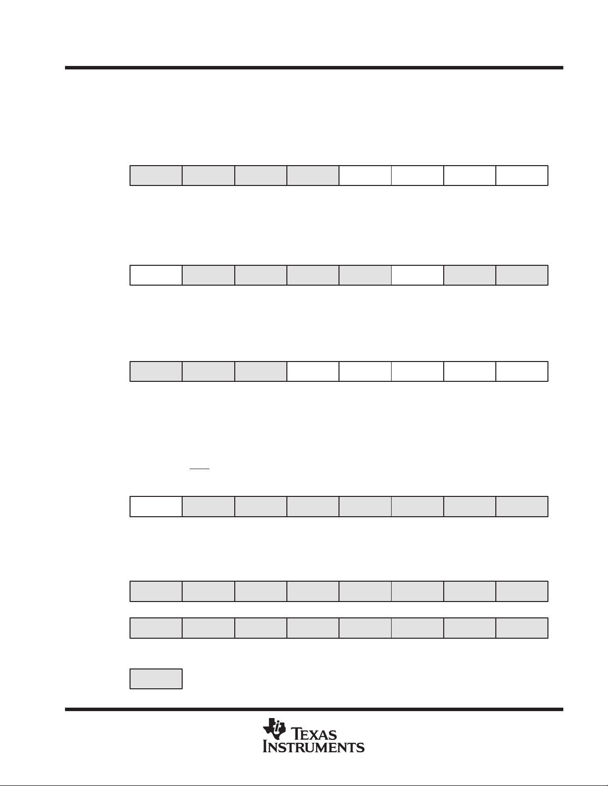
7654 0321
Address
04h
7654 0321
Address
05h
Legend rw:
rw-0:
Bit can be read and written.
Bit can be read and written. It is reset by PUC
SFR bit is not present in device.
 Loading...