


from Texas |
Instruments |
OPA454 |
Burr Brown |
Products |
|
|
|
SBOS391–DECEMBER 2007 |
High-Voltage (100V), High-Current (50mA)
OPERATIONAL AMPLIFIERS, G = 1 Stable
FEATURES
∙WIDE POWER-SUPPLY RANGE: ±5V (10V) to ±50V (100V)
∙HIGH OUTPUT LOAD DRIVE: IO > ±50mA
∙WIDE OUTPUT VOLTAGE SWING: 1V to Rails
∙INDEPENDENT OUTPUT DISABLE OR SHUTDOWN
∙WIDE TEMPERATURE RANGE: –40°C to +85°C
∙PACKAGES: SO and HSOP PowerPAD™
APPLICATIONS
∙TEST EQUIPMENT
∙AVALANCHE PHOTODIODE: High-V Current Sense
∙PIEZOELECTRIC CELLS
∙TRANSDUCER DRIVERS
∙SERVO DRIVERS
∙AUDIO AMPLIFIERS
∙HIGH-VOLTAGE COMPLIANCE CURRENT SOURCES
∙GENERAL HIGH-VOLTAGE REGULATORS/POWER
Status
Flag
V+
Enable/Disable (E/D)
−IN 
OPA454 |
VO |
+IN
Enable/Disable Common
(E/D Com)
V−
DESCRIPTION
The OPA454 is a low-cost operational amplifier with high voltage (100V) and relatively high current drive (25mA). It is unity-gain stable and has a gain-bandwidth product of 2.5MHz.
The OPA454 is internally protected against over-temperature conditions and current overloads. It is fully specified to perform over a wide power-supply range of ±5V to ±50V or on a single supply of 10V to 100V. The status flag is an open-drain output that allows it to be easily referenced to standard low-voltage logic circuitry. This high-voltage op amp provides excellent accuracy, wide output swing, and is free from phase inversion problems that are often found in similar amplifiers.
The output can be independently disabled using the Enable/Disable Pin that has its own common return pin to allow easy interface to low-voltage logic circuitry. This disable is accomplished without disturbing the input signal path, not only saving power but also protecting the load.
Featured in a small exposed metal pad package, the OPA454 is easy to heatsink over the extended industrial temperature range, –40°C to +85°C.
Table 1. OPA454 RELATED PRODUCTS
PRODUCT |
DESCRIPTION |
OPA445 (1) |
80V, 15mA |
OPA452 |
80V, 50mA |
OPA547 |
60V, 750mA |
OPA548 |
60V, 3A |
OPA549 |
60V, 9A |
OPA551 |
60V, 200mA |
OPA567 |
5V, 2A |
OPA569 |
5V, 2.4A |
(1) The OPA445 is pin-compatible with the OPA445, except in applications using the offset trim, and NC pins other than open.
Please be aware that an important notice concerning availability, standard warranty, and use in critical applications of Texas Instruments semiconductor products and disclaimers thereto appears at the end of this data sheet.
PowerPAD is a trademark of Texas Instruments, Inc.
All other trademarks are the property of their respective owners.
PRODUCTION DATA information is current as of publication date. |
Copyright © 2007, Texas Instruments Incorporated |
Products conform to specifications per the terms of the Texas |
|
Instruments standard warranty. Production processing does not |
|
necessarily include testing of all parameters. |
|
OPA454
www.ti.com
SBOS391–DECEMBER 2007
This integrated circuit can be damaged by ESD. Texas Instruments recommends that all integrated circuits be handled with appropriate precautions. Failure to observe proper handling and installation procedures can cause damage.
ESD damage can range from subtle performance degradation to complete device failure. Precision integrated circuits may be more susceptible to damage because very small parametric changes could cause the device not to meet its published specifications.
ORDERING INFORMATION(1)
PRODUCT |
PACKAGE-LEAD |
PACKAGE DESIGNATOR |
PACKAGE MARKING |
OPA454 |
SO-8 |
DDA |
OPA454 |
OPA454 |
HSOP-20(2) |
DWD |
OPA454 |
(1)For the most current package and ordering information see the Package Option Addendum at the end of this document, or see the TI web site at www.ti.com.
(2)Available Q2, 2008.
ABSOLUTE MAXIMUM RATINGS(1)
|
|
|
OPA454 |
UNIT |
Supply Voltage |
|
VS = (V+) – (V–) |
120 |
V |
Signal Input Terminals, Voltage(2) |
|
(V–) – 0.3 to (V+) + 0.3 |
V |
|
Signal Input Terminals, Current(2) |
|
±10 |
mA |
|
E/D to E/D Com Voltage |
|
+5.5 |
V |
|
Output Short-Circuit(3) |
ISC |
Continuous |
|
|
Operating Temperature |
TJ |
–55 to +125 |
°C |
|
Storage Temperature |
|
–55 to +125 |
°C |
|
Junction Temperature |
TJ |
+150 |
°C |
|
|
Human Body Model (HBM) |
|
4000 |
V |
ESD Rating: |
Charged Device Model (CDM) |
|
500 |
V |
|
Machine Model (MM) |
|
150 |
V |
(1)Stresses above these ratings may cause permanent damage. Exposure to absolute maximum conditions for extended periods may degrade device reliability. These are stress ratings only, and functional operation of the device at these or any other conditions beyond those specified is not implied.
(2)Input terminals are diode-clamped to the power-supply rails. Input signals that can swing more than 0.3V beyond the supply rails should be current limited to 10mA or less.
(3)Short-circuit to ground.
|
|
|
|
|
|
PIN ASSIGNMENTS |
|
|
|
|
|
|
|
|
|
DDA PACKAGE |
|
|
|
DWD PACKAGE(1) |
|
|
|
||||||||
SO-8 PowerPAD |
|
|
|
HSOP-20 PowerPAD |
|
|
|
||||||||
(TOP VIEW) |
|
|
|
|
|
|
|||||||||
|
|
|
|
|
(TOP VIEW) |
|
|
|
|||||||
|
|
|
|
|
|
|
|
|
|
|
|
||||
E/D Com (Enable/Disable Common) |
|
|
|
|
|
E/D (Enable/Disable) |
|
|
|
|
|
|
|
|
|
1 |
|
|
8 |
|
V− |
1 |
|
|
|
20 |
V− |
|
|||
|
|
PowerPAD(1) |
|
|
|
|
|
|
|
|
|||||
−IN |
|
|
|
|
V+ |
NC(3) |
|
|
|
|
|
NC(3) |
|||
2 |
|
7 |
|
2 |
|
|
|
19 |
|||||||
Heat Sink |
|
|
|
|
|
||||||||||
|
|
|
|
|
|
|
|
|
|
|
|
|
|
|
|
+IN |
|
(Located on |
|
|
|
OUT |
NC |
(3) |
3 |
|
|
|
18 |
NC |
(3) |
3 |
|
6 |
|
|
|
|
|||||||||
bottom side) |
|
|
|
|
|
|
|
||||||||
V− |
4 |
|
|
5 |
|
Status Flag |
V− |
4 |
|
|
|
17 |
Status Flag |
||
|
|
|
|
|
|
|
PowerPAD(2) |
|
|
|
|
||||
|
|
|
|
|
|
|
+IN |
5 |
|
Heat Sink |
|
16 |
VOUT |
||
|
|
|
|
|
|
|
|
|
|
|
|||||
(1) PowerPAD is internally connected |
to |
V–. |
NC(3) |
6 |
|
(Located on |
|
15 |
V+ |
|
|||||
|
|
|
|
top side) |
|
|
|
|
|||||||
Soldering the PowerPAD to the PCB is |
−IN |
7 |
|
|
|
14 |
NC(3) |
||||||||
|
|
|
|
|
|
|
|
|
|||||||
always required, even with applications that |
NC(3) |
8 |
|
|
|
13 |
NC(3) |
||||||||
have low power dissipation. |
|
|
|
E/D Com (Enable/Disable Common) |
9 |
|
|
|
12 |
E/D (Enable/Disable) |
|||||
|
|
|
|
|
|
|
V− |
10 |
|
|
|
11 |
V− |
|
|
|
|
|
|
|
|
|
|
|
|
|
|
|
|
|
|
(1) Available Q2, 2008.
(2) PowerPAD is internally connected to V–.
(3) NC = No internal connection
2 |
Submit Documentation Feedback |
Copyright © 2007, Texas Instruments Incorporated |
Product Folder Link(s): OPA454

OPA454
www.ti.com
SBOS391–DECEMBER 2007
ELECTRICAL CHARACTERISTICS: VS = ±50V
Boldface limits apply over the specified temperature range, TA = –40°C to +85°C.
At TP(1) = +25°C, RL = 4.8kΩ to mid-supply, VCM = VOUT = mid-supply, unless otherwise noted.
PARAMETER |
|
CONDITIONS |
OFFSET VOLTAGE |
|
|
Input Offset Voltage |
VOS |
IO = 0 |
vs Temperature(2) |
dVOS/dT |
|
vs Power Supply |
PSRR |
VS = ±4V to ±60V, VCM = 0V |
INPUT BIAS CURRENT |
|
|
Input Bias Current |
IB |
|
vs Temperature |
|
|
Input Offset Current |
IOS |
|
NOISE |
|
|
Input Voltage Noise Density, f = 10Hz |
en |
|
Input Voltage Noise Density, f = 10kHz |
|
|
f = 0.01Hz to 10Hz |
|
|
Current Noise Density, f = 1kHz |
in |
|
INPUT VOLTAGE RANGE |
|
|
Common-Mode Voltage Range |
VCM |
Linear Operation |
Common-Mode Rejection |
CMRR |
VS = ±50V, –25V ≤ VCM ≤ +25V |
|
|
VS = ±50V, –45V ≤ VCM ≤ +45V |
Over Temperature |
|
VS = ±50V, –25V ≤ VCM ≤ +25V |
Over Temperature |
|
VS = ±50V, –45V ≤ VCM ≤ +45V |
INPUT IMPEDANCE |
|
|
Differential |
|
|
Common-Mode |
|
|
OPEN-LOOP GAIN |
|
|
Open-Loop Voltage Gain(4) |
AOL |
|
|
|
(V–) + 1V < VO < (V+) – 1V, |
|
|
RL = 49kΩ, IO = ±1mA |
|
|
(V–) + 1V < VO < (V+) – 1V, |
|
|
RL = 49kΩ, IO = ±1mA |
|
|
(V–) + 1V < VO < (V+) – 2V, |
|
|
RL = 4.8kΩ, IO = ±10mA |
|
|
(V–) + 1V < VO < (V+) – 2V, |
|
|
RL = 4.8kΩ, IO = ±10mA |
|
|
(V–) + 2V < VO < (V+) – 3V, |
|
|
RL = 1880Ω, IO = ±25mA |
|
|
(V–) + 2V < VO < (V+) – 3V, |
|
|
RL = 1880Ω, IO = ±25mA |
|
OPA454 |
|
|
MIN |
TYP |
MAX |
UNIT |
|
±0.2 |
±4 |
mV |
|
±1.6 |
±10 |
μV/°C |
|
25 |
100 |
μV/V |
|
±1.4 |
±100 |
pA |
See Typical Characteristics |
|
||
|
±0.2 |
±100 |
pA |
|
300 |
|
nV/√Hz |
|
35 |
|
nV/√Hz |
|
15 |
|
μVPP |
|
40 |
|
fA/√Hz |
(V–) + 2.5 |
See Note (3) |
(V+) – 2.5 |
V |
100 |
146 |
|
dB |
100 |
147 |
|
dB |
80 |
88 |
|
dB |
72 |
82 |
|
dB |
|
1013 || 10 |
|
Ω || pF |
|
1013 || 9 |
|
Ω || pF |
100 |
130 |
|
dB |
|
112 |
|
dB |
100 |
115 |
|
dB |
|
106 |
|
dB |
80 |
102 |
|
dB |
|
84 |
|
dB |
(1)TP is the temperature of the leadframe die pad (exposed thermal pad) of the PowerPAD package.
(2)See typical characteristic curve, Offset Voltage Drift Production Distribution (Figure 14).
(3)Typical range is (V–) + 1.5V to (V+) – 1.5V.
(4)Measured using low-frequency (<10Hz) ±49V square wave. See typical characteristic curve, Current Limit vs Temperature (Figure 24).
Copyright © 2007, Texas Instruments Incorporated |
Submit Documentation Feedback |
3 |
Product Folder Link(s): OPA454

OPA454
www.ti.com
SBOS391–DECEMBER 2007
ELECTRICAL CHARACTERISTICS: VS = ±50V (continued)
Boldface limits apply over the specified temperature range, TA = –40°C to +85°C.
At TP = +25°C, RL = 4.8kΩ to mid-supply, VCM = VOUT = mid-supply, unless otherwise noted.
PARAMETER |
|
CONDITIONS |
FREQUENCY RESPONSE(5) |
|
|
Gain-Bandwidth Product |
GBW |
Small-Signal |
Slew Rate |
SR |
G = ±1, VO = 80V Step, RL = 3.27kΩ |
Full-Power Bandwidth(6) |
|
|
Settling Time: ±0.1%(7) |
|
G = ±1, VO = 20V Step |
Settling Time: ±0.01%(7) |
|
G = ±5 or ±10, VO = 80V Step |
Total Harmonic Distortion + Noise(8) |
THD+N |
VS = +40.6V/–39.6V, G = ±1, |
|
|
f = 1kHz, VO = 77.2VPP |
OUTPUT |
|
|
 Voltage Output Swing From Rail(9)
 Continuous Current Output, dc
Maximum Peak Current Output, Current Limit(10)
Over Temperature
VO |
RL = 49kΩ, AOL ≥ 100dB, IO = 1mA |
|
RL = 4.8kΩ, AOL ≥ 100dB, IO = 10mA |
|
RL = 1880Ω, AOL ≥ 80dB, IO = 26mA |
|
Depends on Circuit Conditions |
IO |
|
Capacitive Load Drive(5) |
CLOAD |
Open-Loop Output Impedance |
RO |
Output Disabled |
|
Output Capacitance |
|
Feedthrough Capacitance(11)
 STATUS FLAG PIN (Referenced to E/D Com)(12)
Status Flag Delay |
Enable → Disable |
|
Disable → Enable |
|
Over-Current Delay(13) |
|
Over-Current Recovery Delay(13) |
Junction Temperature |
TJ |
Alarm (status flag high) |
|
Return to Normal Operation (status flag low) |
|
Output Voltage(5) |
Normal Operation |
|
RL = 100Ω During Thermal Overdrive, |
|
Alarm |
|
OPA454 |
|
|
MIN |
TYP |
MAX |
UNIT |
|
2.5 |
|
MHz |
|
13 |
|
V/μs |
|
35 |
|
kHz |
|
3 |
|
μs |
|
10 |
|
μs |
|
0.0008 |
|
% |
(V–) + 1 |
|
(V+) – 1 |
V |
(V–) + 1 |
|
(V+) – 2 |
V |
(V–) + 2 |
|
(V+) – 3 |
V |
|
See Figure 6 |
|
|
|
+120/–150 |
|
mA |
|
+140/–170 |
|
mA |
|
200 |
|
pF |
|
See Figure 5 |
|
Ω |
|
18 |
|
pF |
|
150 |
|
fF |
|
6 |
|
μs |
|
4 |
|
μs |
|
15 |
|
μs |
|
10 |
|
μs |
|
+150 |
|
°C |
|
+130 |
|
°C |
|
|
E/D Com + 2 |
V |
(V+) – 2.5 |
|
|
V |
(5)See Typical Characteristic curves.
(6)See typical characteristic curve, Maximum Output Voltage vs Frequency (Figure 12).
(7)See the Applications Information section, Settling Time.
(8)Supplies reduced to allow closer swing to rails due to test equipment limitations. See typical characteristic curve Total Harmonic Distortion + Noise vs Temperature (Figure 30 and Figure 31) for additional power levels.
(9)See typical characteristic curve, Output Voltage Swing vs Output Current (Figure 11).
(10)Measured using low-frequency (<10Hz) ±49V square wave. See typical characteristic curve, Current Limit vs Temperature (Figure 24).
(11)Measured using Figure 1.
(12)100kΩ pull-up resistor to (V+). E/D common to (V–). Status flag indicates an over temperature or over-current condition.
(13)See Typical Characteristic curves for current limit behavior.
4 |
Submit Documentation Feedback |
Copyright © 2007, Texas Instruments Incorporated |
Product Folder Link(s): OPA454

OPA454
www.ti.com
SBOS391–DECEMBER 2007
ELECTRICAL CHARACTERISTICS: VS = ±50V (continued)
Boldface limits apply over the specified temperature range, TA = –40°C to +85°C.
At TP = +25°C, RL = 4.8kΩ to mid-supply, VCM = VOUT = mid-supply, unless otherwise noted.
|
|
|
|
OPA454 |
|
|
PARAMETER |
|
CONDITIONS |
MIN |
TYP |
MAX |
UNIT |
E/D (ENABLE/DISABLE) PIN |
|
|
|
|
|
|
E/D Pin, Referenced to E/D Com Pin(14)(15) |
|
|
|
|
|
|
High (output enabled) |
VSD |
Pin Open or Forced High |
E/D Com + 2.5 |
|
E/D Com + 5 |
V |
Low (output disabled) |
VSD |
Pin Forced Low |
E/D Com |
|
E/D Com + |
V |
|
0.65 |
|||||
|
|
|
|
|
|
|
Output Disable Time |
|
|
|
4 |
|
μs |
Output Enable Time |
|
|
|
3 |
|
μs |
E/D COM PIN |
|
|
|
|
|
|
Voltage Range |
|
|
(V–) |
|
(V+) – 5 |
V |
POWER SUPPLY |
|
|
|
|
|
|
Specified Range |
VS |
|
|
±50 |
|
V |
Operating Voltage Range |
|
|
±5 |
|
±50 |
V |
Quiescent Current |
IQ |
IO = 0 |
|
3.2 |
4 |
mA |
Quiescent Current in Shutdown Mode |
|
IO = 0, VE/D = 0.65V |
|
150 |
210 |
μA |
TEMPERATURE RANGE |
|
|
|
|
|
|
Specified Range |
TA |
|
–40 |
|
+85 |
°C |
Operating Range |
TA |
|
–55 |
|
+125 |
°C |
Thermal Resistance, Junction-to-Case(16) |
|
|
|
|
|
|
SO-8 PowerPAD(17) |
θJC |
|
|
10 |
|
°C/W |
HSOP-20 |
|
|
|
10 |
|
°C/W |
Thermal Resistance, Junction-to-Ambient |
θJA |
|
|
|
|
|
SO-8 PowerPAD(17) |
|
|
|
24/52 |
|
°C/W |
HSOP-20(18) |
|
|
|
65 |
|
°C/W |
(14)See typical characteristic curve, IENABLE vs VENABLE (Figure 46).
(15)High enables the outputs.
(16)TP is the temperature of the leadframe die pad (exposed thermal pad) of the PowerPAD package.
(17)Lower value is for land area of 1-inch × 1-inch, 2-oz copper. Upper value is for exposed-pad sized area of 1-oz copper.
(18)Value given is for DW-20 package, similar to the DWD package, but without an exposed pad. Actual θJA may approach θJC by selection of external heatsink and airflow.
+50V
E/D
VOUT
RL 50kΩ
100VPP |
|
|
|
|
E/D Com |
||
10kHz |
|
|
|
|
|
|
|
|
|
|
|
||||
|
−50V |
||||||
Figure 1. Feedthrough Capacitance Circuit
Copyright © 2007, Texas Instruments Incorporated |
Submit Documentation Feedback |
5 |
Product Folder Link(s): OPA454

OPA454
www.ti.com
SBOS391–DECEMBER 2007
TYPICAL CHARACTERISTICS
At TP = +25°C, VS = ±50V, and RL = 4.8kΩ connected to GND, unless otherwise noted.
OPEN-LOOP GAIN AND PHASE vs FREQUENCY
|
180 |
|
|
|
|
|
|
|
|
|
|
|
|
|
|
|
|
|
|
|
|
|
|
|
|
|
|
|
|
|
|
|
|
|
|
|
|
|
|
|
|
|
|
|
|
|
|
|
|
|
|
|
|
|
|
|
|
|
|
|
|
|
|
|
|
|
|
|
|
|
|
|
|
|
|
|
|
|
|
|
|
|
|
|
|
|
|
|
|
°) |
160 |
|
|
|
|
|
|
|
|
|
|
|
|
|
|
|
|
|
|
|
|
|
|
|
|
|
|
|
|
|
|
|
|
|
|
|
|
|
|
|
|
|
|
|
|
|
|
|
|
|
|
|
|
|
|
|
|
|
|
|
|
|
|
|
|
|
|
|
|
|
|
|
|
|
|
|
|
|
|
|
|
|
|
|
|
|
|
||
|
|
|
|
|
|
|
|
|
|
|
|
|
|
|
|
|
|
|
|
|
|
|
|
|
|
|
|
|
|
|
|
|
|
|
|
|
|
|
|
|
|
|
|
|
(dB, |
140 |
|
|
|
|
|
|
|
|
|
|
|
|
|
|
|
|
|
|
|
|
|
|
|
|
|
|
|
|
|
|
|
|
|
|
|
|
|
|
|
|
|
|
|
Phase |
120 |
|
|
|
|
|
|
|
|
|
|
|
|
|
|
|
|
|
|
|
|
|
|
|
|
|
|
|
|
|
|
|
|
|
|
|
|
|
|
|
|
|
|
|
|
|
|
|
|
|
|
|
|
|
|
|
|
|
|
|
|
|
|
|
|
|
|
|
|
|
|
|
|
|
|
|
|
|
|
|
|
|
|
|
|
|
|
||
100 |
|
|
|
|
|
|
|
|
|
|
|
|
|
|
|
|
|
|
|
|
|
|
|
|
|
|
|
|
|
|
|
|
|
|
|
|
|
|
|
|
|
|
|
|
LoopGain, |
|
|
|
|
|
|
|
|
|
|
|
|
|
|
|
|
|
|
|
|
|
|
|
|
|
|
|
|
|
|
|
|
|
|
|
|
|
Phase |
|
|
||||
40 |
|
|
|
|
|
|
|
|
|
|
|
|
|
|
|
|
|
|
|
|
|
|
|
|
|
|
|
|
|
|
|
|
|
|
|
|
|
|
|
|||||
|
80 |
|
|
|
|
|
|
|
|
|
|
|
|
|
|
|
|
|
|
|
|
|
|
|
|
|
|
|
|
|
|
|
|
|
|
|
|
|
|
|
|
|
|
|
- |
60 |
|
|
|
|
|
|
|
|
|
|
|
|
|
|
|
|
|
|
|
|
|
|
|
|
|
|
|
|
|
|
|
|
|
|
|
|
|
|
|
|
|
|
|
|
|
|
|
|
|
|
|
|
|
|
|
|
|
|
|
|
|
|
|
|
|
|
|
|
|
|
|
|
|
|
|
|
|
|
|
|
|
|
|
|
|
|
||
|
|
|
|
|
|
|
|
|
|
|
|
|
|
|
|
|
|
|
|
|
|
|
|
|
|
|
|
|
|
|
|
|
|
|
|
|
|
|
|
|
|
|
|
|
|
|
|
|
|
|
|
|
|
|
|
|
|
|
|
|
|
|
|
|
|
|
|
|
|
|
Gain |
|
|
|
|
|
|
|
|
|
|
|
|
|
|
||||
|
|
CLOAD |
= 50pF |
|
|
|
|
|
|
|
|
|
|
|
|
|
|
|
|
|
|
|
|
|
|
|
|
|
|
|
|
|
|
|||||||||||
Open |
|
|
|
|
|
|
|
|
|
|
|
|
|
|
|
|
|
|
|
|
|
|
|
|
|
|
|
|
|
|
|
|
||||||||||||
|
20 |
|
RLOAD |
= 4.87kΩ |
|
|
|
|
|
|
|
|
|
|
|
|
|
|
|
|
|
|
|
|
|
|
|
|
|
|
|
|
|
|
||||||||||
|
|
|
|
|
|
|
|
|
|
|
|
|
|
|
|
|
|
|
|
|
|
|
|
|
|
|
|
|
|
|
|
|
|
|
|
|
|
|
|
|
|
|
|
|
|
0 |
|
VCM |
= 0V |
|
|
|
|
|
|
|
|
|
|
|
|
|
|
|
|
|
|
|
|
|
|
|
|
|
|
|
|
|
|
|
|
|
|
||||||
|
|
|
|
|
|
|
|
|
|
|
|
|
|
|
|
|
|
|
|
|
|
|
|
|
|
|
|
|
|
|
|
|
|
|
|
|||||||||
|
|
|
|
|
|
|
|
|
|
|
|
|
|
|
|
|
|
|
|
|
|
|
|
|
|
|
|
|
|
|
|
|
|
|
|
|
||||||||
|
−20 |
|
|
|
|
|
|
|
|
|
|
|
|
|
|
|
|
|
|
|
|
|
|
|
|
|
|
|
|
|
|
|
|
|
|
|
|
|
|
|
|
|
|
|
|
0.1 |
|
|
1 |
|
|
10 |
|
|
100 |
|
|
1k |
10k |
100k |
1M |
10M |
|||||||||||||||||||||||||||
|
|
|
|
|
|
|
|
|
|
|||||||||||||||||||||||||||||||||||
Frequency (Hz)
Figure 2.
UNITY-GAIN BANDWIDTH vs TEMPERATURE
|
3.8 |
|
|
|
|
|
|
|
|
|
3.6 |
|
|
|
|
|
|
|
|
|
3.4 |
|
|
|
|
|
|
|
|
Bandwidth(MHz) |
3.2 |
|
|
VCM = 0V |
|
|
|
|
|
3.0 |
|
|
|
|
|
|
|
||
|
|
|
|
|
|
|
|
||
2.8 |
|
|
|
|
|
|
VCM = 45V |
||
2.6 |
|
|
|
|
|
|
|||
VCM = −45V |
|
|
|
|
|
|
|||
|
|
|
|
|
|
|
|||
|
|
|
|
|
|
|
|
||
|
2.4 |
|
|
|
|
|
|
|
|
|
2.2 |
|
|
|
|
|
|
|
|
|
CL = 30pF. 100pF, and 200pF |
|
|
|
|
||||
|
2.0 |
|
|
|
|
|
|
|
|
|
−75 |
−50 |
−25 |
0 |
25 |
50 |
75 |
100 |
125 |
|
|
|
Exposed Thermal Pad Temperature (°C) |
|
|||||
Figure 4.
OPEN-LOOP GAIN vs PEAK-LOAD CURRENT
|
140 |
|
|
|
|
|
|
|
|
|
|
|
|
|
|
|
|
|
|
|
|
|
|
|
|
|
|
|
|
|
130 |
|
|
|
|
|
|
|
|
|
|
|
|
|
|
|
|
VS = |
±50V |
|
|
|
|
|
|
|
|||
|
|
|
|
|
|
|
|
|
|
|
||||
|
120 |
|
|
|
|
|
|
|
|
|
|
|
|
|
|
|
|
|
|
|
|
|
|
|
|
|
|
|
|
(dB) |
110 |
|
|
|
|
|
|
|
|
|
|
|
|
|
|
|
|
|
|
|
|
|
|
|
|
|
|
||
100 |
|
|
|
|
|
|
|
|
VS |
= ±15V |
|
|
||
OL |
|
|
|
|
|
|
|
|
|
|
|
|
|
|
|
|
|
|
|
|
|
|
|
|
|
|
|
|
|
A |
|
|
|
|
|
|
|
|
|
|
|
|
|
|
|
90 |
|
|
|
|
|
|
|
|
|
|
|
|
|
|
|
|
|
V |
S = ±4V |
|
|
|
|
|
|
|
||
|
80 |
|
|
|
|
|
|
|
|
|
|
|
|
|
|
|
|
|
|
|
|
|
|
|
|
|
|
|
|
|
70 |
|
|
|
|
|
|
|
|
|
|
|
|
|
|
|
|
|
|
|
|
|
|
|
|
|
|
|
|
|
60 |
|
|
|
|
|
|
|
|
|
|
|
|
|
|
|
|
|
|
|
|
|
|
|
|
|
|
|
|
|
0 |
5 |
10 |
15 |
20 |
25 |
||||||||
Peak IL (mA)
Figure 6.
PHASE MARGIN vs TEMPERATURE
|
70 |
|
|
|
|
|
|
|
|
CL = 30pF |
|
|
|
|
|
VCM = −45V |
|
|
65 |
|
|
|
|
|
VCM = 0V |
|
|
|
|
|
|
|
|
VCM = +45V |
|
(°) |
60 |
|
|
|
|
|
|
|
PhaseMargin |
55 |
|
|
|
|
|
|
|
50 |
|
|
|
|
|
|
|
|
|
|
|
|
|
|
|
|
|
|
CL = 100pF |
C |
L |
= 200pF |
|
|
|
|
|
45 |
|
|
|
|
|
|
|
|
40 |
|
|
|
|
|
|
|
|
−75 −50 −25 |
0 |
|
25 |
50 |
75 |
100 |
125 |
|
Exposed Thermal Pad Temperature (°C) |
|
||||||
Figure 3.
OPEN-LOOP OUTPUT IMPEDANCE vs FREQUENCY
|
1M |
|
(Ω) |
100k |
|
Impedance |
||
10k |
||
LoopOutput |
||
1k |
||
|
||
|
100 |
|
- |
|
|
Open |
10 |
|
|
||
|
1 |
1 |
10 |
100 |
1k |
10k |
100k |
1M |
10M |
Frequency (Hz)
Figure 5.
OPEN-LOOP GAIN vs TEMPERATURE
|
140 |
|
|
|
|
|
|
|
|
|
|
|
|
|
130 |
|
|
|
|
|
|
|
|
|
|
|
|
|
120 |
|
|
|
|
|
|
|
|
|
|
|
|
|
110 |
|
|
|
|
|
|
|
|
|
|
|
|
(dB) |
|
RLOAD = 48kΩ |
|
|
|
|
|
|
|
|
|
|
|
100 |
VOUT = ±49V (dc) |
|
|
|
|
|
|
|
|
|
|||
|
IOUT |
= ±1mA |
|
|
|
|
|
|
|
|
|
|
|
OL |
|
|
|
|
|
|
|
|
|
|
|
||
90 |
|
|
|
|
|
|
|
|
|
|
|
|
|
A |
|
|
|
RL = 4.8kΩ |
|
|
|
|
|
|
|
||
|
|
|
|
|
|
|
|
|
|
|
|||
|
|
|
|
|
|
|
|
|
|
|
|
||
|
80 |
|
VOUT = +48V, −49V (dc) |
|
|
|
|
|
|
|
|||
|
70 |
|
IOUT = +9.9mA to −10mA |
|
|
|
|
|
|
|
|||
|
|
RL = 1.88kΩ |
|
|
R |
|
= 900Ω |
|
|
|
|||
|
|
|
|
|
L |
|
|
|
|||||
|
|
|
VOUT = +47V, −48V (dc) |
|
|
|
|
|
|
||||
|
60 |
|
VOUT = +45V, −47V (dc) |
|
|||||||||
|
|
|
IOUT = ±25mA |
|
I |
|
|
= 50mA to −52mA |
|
||||
|
|
|
|
|
|
|
OUT |
|
|
|
|
||
|
50 |
|
|
|
|
|
|
|
|
|
|
|
|
|
|
−75 |
−50 |
−25 |
0 |
25 |
|
|
50 |
75 |
100 |
125 |
|
Exposed Thermal Pad Temperature (°C)
Figure 7.
6 |
Submit Documentation Feedback |
Copyright © 2007, Texas Instruments Incorporated |
Product Folder Link(s): OPA454

OPA454
www.ti.com
SBOS391–DECEMBER 2007
TYPICAL CHARACTERISTICS (continued)
At TP = +25°C, VS = ±50V, and RL = 4.8kΩ connected to GND, unless otherwise noted.
COMMON-MODE REJECTION RATIO vs FREQUENCY
|
140 |
|
|
|
|
|
|
|
|
|
|
|
|
|
|
|
|
|
|
|
|
|
|
|
|
|
|
|
|
|
|
|
|
|
|
|
|
|
|
|
|
|
|
|
|
|
|
|
|
|
|
|
|
|
|
|
|
|
|
|
|
|
|
|
|
|
|
|
|
|
|
|
|
|
|
|
|
|
120 |
|
|
|
|
|
|
|
|
|
|
|
|
|
|
|
|
|
|
|
|
|
|
|
|
|
|
|
|
|
|
|
|
|
|
|
|
|
|
|
|
|
|
|
|
|
|
|
|
|
|
|
|
|
|
|
|
|
|
|
|
|
|
|
|
|
|
|
|
|
|
|
|
|
|
|
|
CMRR(dB) |
100 |
|
|
|
|
|
|
|
|
|
|
|
|
|
|
|
|
|
|
|
|
|
|
|
|
|
|
|
|
|
|
|
|
|
|
|
|
|
|
|
|
|
|
|
|
|
|
|
|
|
|
|
|
|
|
|
|
|
|
|
|
|
|
|
|
|
|
|
|
|
|
|
|
|
|
||
80 |
|
|
|
|
|
|
|
|
|
|
|
|
|
|
|
|
|
|
|
|
|
|
|
|
|
|
|
|
|
|
|
|
|
|
|
|
|
|
|
|
|
|
|
|
|
|
|
|
|
|
|
|
|
|
|
|
|
|
|
|
|
|
|
|
|
|
|
|
|
|
|
|
|
|
|
||
|
|
|
|
|
|
|
|
|
|
|
|
|
|
|
|
|
|
|
|
|
|
|
|
|
|
|
|
VCM = −45V |
|
|||||||||
60 |
|
|
|
|
|
|
|
|
|
|
|
|
|
|
|
|
|
|
|
|
|
|
|
|
|
|
|
|
|
|
|
|
|
|
|
|
|
|
|
|
|
|
|
|
|
|
|
|
|
|
|
|
|
|
|
|
|
|
|
|
|
|
|
|
|
|
|
|
|
|
|
|
|
|
|
||
|
|
|
|
|
|
|
|
|
|
|
|
|
|
|
|
|
|
|
|
|
|
|
|
|
|
|
|
|
|
|
|
|
|
|
|
|
|
|
|
40 |
|
|
|
|
|
|
|
|
|
|
|
|
|
|
|
|
|
|
|
|
|
|
|
|
|
|
|
|
|
|
|
|
|
|
|
|
|
|
|
|
|
|
|
|
|
|
|
|
|
|
|
|
|
|
|
|
|
|
|
VCM = +45V |
|
|
|
|
|
|
|
|
||||||||
|
|
|
|
|
|
|
|
|
|
|
|
|
|
|
|
|
|
|
|
|
|
|
|
|
|
|
|
|
|
|
||||||||
|
20 |
|
|
|
|
|
|
|
|
|
|
|
|
|
|
|
|
|
|
|
|
|
|
|
|
|
|
|
|
|
|
|
|
|
|
|
|
|
|
|
|
|
|
|
|
|
|
|
|
|
|
|
|
|
|
|
|
|
|
|
|
|
|
|
|
|
|
|
|
|
|
|
|
|
|
|
|
|
0 |
|
|
|
|
|
|
|
|
|
|
|
|
|
|
|
|
|
|
|
|
|
|
|
|
|
|
|
|
|
|
|
|
|
|
|
|
|
|
|
|
|
|
|
|
|
|
|
|
|
|
|
|
|
|
|
|
|
|
|
|
|
|
|
|
|
|
|
|
|
|
|
|
|
|
|
|
|
0.001 |
|
0.01 |
0.1 |
|
|
1 |
10 |
|
100 |
|
|
|
|
1k |
10k |
||||||||||||||||||
|
|
|
|
|
|
|
|
|
|
|
|
|
Frequency (Hz) |
|
|
|
|
|
|
|
|
|
|
|
|
|
|
|||||||
|
|
|
|
|
|
|
|
|
|
|
|
|
|
Figure 8. |
|
|
|
|
|
|
|
|
|
|
|
|
|
|
||||||
|
POWER-SUPPLY REJECTION RATIO vs FREQUENCY |
|||||||||||||||||||||||||||||||||
|
140 |
|
|
|
|
|
|
|
|
|
|
|
|
|
|
|
|
|
|
|
|
|
|
|
|
|
|
|
|
|
|
|
|
|
|
|
|
|
|
|
|
|
|
|
|
|
|
|
|
|
|
|
|
|
|
|
|
|
|
|
|
|
|
|
|
|
|
|
|
|
120 |
|
|
|
|
|
|
|
|
|
|
|
|
|
|
|
|
|
|
|
|
|
|
|
|
|
|
|
|
|
|
|
|
|
|
|
|
|
|
|
|
|
|
|
|
|
|
|
|
|
|
|
|
|
|
|
|
|
|
|
|
|
|
|
|
|
|
|
|
PSRR(dB) |
100 |
|
|
|
|
|
|
|
|
|
|
|
|
|
|
|
|
|
|
|
|
|
|
|
|
|
|
|
|
|
|
|
|
|
|
|
|
|
|
|
|
|
|
|
|
|
|
|
|
|
|
|
|
|
|
|
|
|
|
|
|
|
|
|
|
|
|
||
80 |
|
|
|
|
|
|
|
|
|
|
|
|
|
|
|
|
|
|
|
|
|
|
|
|
|
|
|
|
|
|
|
|
|
|
|
|
|
|
|
|
|
|
|
|
|
|
|
|
|
|
|
|
|
|
|
|
|
|
|
|
|
|
|
|
|
|
|
|
|
|
60 |
|
|
|
|
|
|
|
|
|
|
|
|
|
|
|
|
|
|
|
|
|
|
|
|
|
|
|
|
|
|
|
|
|
|
|
|
|
|
|
|
|
|
|
|
|
|
|
|
|
|
|
|
|
|
|
|
|
|
|
|
|
|
|
|
|
|
|
|
|
40 |
|
|
|
|
|
|
|
|
|
|
|
|
|
|
|
|
|
|
|
|
|
|
|
|
|
|
|
|
|
|
|
|
|
|
|
|
|
|
|
|
|
|
|
|
|
|
|
|
|
|
|
|
|
|
|
|
|
|
|
|
|
|
|
|
|
|
|
|
|
20 |
|
|
|
|
|
|
|
|
|
|
|
|
|
|
|
|
|
|
|
|
|
|
|
|
|
|
|
|
|
|
|
|
|
|
|
|
|
|
|
|
|
|
|
|
|
|
|
|
|
|
|
|
|
|
|
|
|
|
|
|
|
|
|
|
|
|
|
|
|
0 |
|
|
|
|
|
|
|
|
|
|
|
|
|
|
|
|
|
|
|
|
|
|
|
|
|
|
|
|
|
|
|
|
|
|
|
|
|
|
|
|
|
|
|
|
|
|
|
|
|
|
|
|
|
|
|
|
|
|
|
|
|
|
|
|
|
|
|
|
|
1 |
|
10 |
100 |
|
|
|
1k |
10k |
|
100k |
1M |
||||||||||||||||||||||
|
|
|
|
|
|
|
|
|
|
|
|
|
Frequency (Hz) |
|
|
|
|
|
|
|
|
|
|
|
|
|
|
|||||||
|
|
|
|
|
|
|
|
|
|
|
|
|
|
Figure 10. |
|
|
|
|
|
|
|
|
|
|
|
|
|
|
||||||
|
|
MAXIMUM OUTPUT VOLTAGE vs FREQUENCY |
|
|
|
|||||||||||||||||||||||||||||
|
120 |
|
|
|
|
|
|
|
|
|
|
|
|
|
|
|
|
|
|
|
|
|
|
|
|
|
|
|
|
|
|
|
|
|
|
|
|
|
|
|
|
|
|
|
|
|
|
|
|
|
|
|
|
|
|
|
|
|
|
VOUT = ±49V |
|
|
|||||||
|
100 |
|
|
|
|
|
|
|
|
|
|
|
|
|
|
|
|
|
|
|
|
|
|
|
|
RL = 4.8kΩ |
|
|
||||||
|
|
|
|
|
|
|
|
|
|
|
|
|
|
|
|
|
|
|
|
|
|
|
|
|
|
|||||||||
) |
|
|
|
|
|
|
|
|
|
|
|
|
|
|
|
|
|
|
|
|
|
|
|
|
IOUT = ±10mA |
|
|
|||||||
PP |
|
|
|
|
|
|
|
|
|
|
|
|
|
|
|
|
|
|
|
|
|
|
|
|
|
|
|
|
|
|
|
|
|
|
|
|
|
|
|
|
|
|
|
|
|
|
|
|
|
|
|
|
|
|
|
|
|
|
|
|
|
|
|
|
|
|
|
|
|
(V |
80 |
|
|
|
|
|
|
|
|
|
|
|
|
|
|
|
|
|
|
|
|
|
|
|
|
|
|
|
|
|
|
|
|
|
|
|
|
|
|
|
|
|
|
|
|
|
|
|
|
|
|
|
|
|
|
|
|
|
|
|
|
|
|
|
|
|
|
||
|
|
|
|
|
|
|
|
|
|
|
|
|
|
|
|
|
|
|
|
|
|
|
|
|
|
|
|
|
|
|
|
|
|
|
OutputVoltage |
60 |
|
|
|
|
|
|
|
|
|
|
|
|
|
|
|
|
|
|
|
|
|
|
|
|
|
|
|
|
|
|
|
|
|
|
|
|
|
|
|
|
|
|
|
|
|
|
|
|
|
|
|
|
|
|
|
|
|
|
|
|
|
|
|
|
|
|
|
|
|
40 |
|
|
|
|
|
|
|
|
|
|
|
|
|
|
|
|
|
|
|
|
|
|
|
|
|
|
|
|
|
|
|
|
|
|
|
|
|
|
|
|
|
|
|
|
|
|
|
|
|
|
|
|
|
|
|
|
|
|
|
|
|
|
|
|
|
|
|
|
|
20 |
|
|
|
|
|
|
|
|
|
|
|
|
|
|
|
|
|
|
|
|
|
|
|
|
|
|
|
|
|
|
|
|
|
|
|
|
|
|
|
|
|
|
|
|
|
|
|
|
|
|
|
|
|
|
|
|
|
|
|
|
|
|
|
|
|
|
|
|
|
0 |
|
|
|
|
|
|
|
|
|
|
|
|
|
|
|
|
|
|
|
|
|
|
|
|
|
|
|
|
|
|
|
|
|
|
|
|
|
|
|
|
|
|
|
|
|
|
|
|
|
|
|
|
|
|
|
|
|
|
|
|
|
|
|
|
|
|
|
|
|
0 |
|
50 |
100 |
|
|
|
150 |
|
|
200 |
|
250 |
|
|
300 |
||||||||||||||||||
|
|
|
|
|
|
|
|
|
|
|
|
|
Frequency (kHz) |
|
|
|
|
|
|
|
|
|
|
|||||||||||
Figure 12.
POWER-SUPPLY AND COMMON-MODE
REJECTION RATIO vs TEMPERATURE
|
120 |
|
|
|
|
|
|
|
|
|
|
PSRR |
|
|
|
|
|
|
|
|
100 |
|
|
|
|
|
1kHz, CMRR |
||
(dB) |
|
|
|
|
|
|
|||
80 |
10kHz, CMRR |
|
|
|
|
|
|||
|
|
|
|
|
|
|
|
||
CMRR |
|
|
|
|
|
|
|
|
|
60 |
|
|
|
|
|
100kHz, CMRR |
|
||
PSRRand |
|
|
|
|
|
|
|
||
40 |
|
|
|
|
1.3MHz, CMRR |
|
|
||
|
|
|
|
|
|
|
|||
|
|
|
|
|
|
|
|
|
|
|
20 |
VCM |
= +45V |
|
|
|
|
|
|
|
|
|
|
|
|
|
|
||
|
|
VCM = −45V |
|
|
|
|
|
|
|
|
0 |
|
|
|
|
|
|
|
|
|
−75 |
−50 |
−25 |
0 |
25 |
50 |
75 |
100 |
125 |
|
|
Exposed Thermal Pad Temperature (°C) |
|
|
|||||
Figure 9.
OUTPUT VOLTAGE SWING vs OUTPUT CURRENT (Measured When Status Flag Transitions From Low to High)
|
50 |
|
|
|
|
|
|
|
|
|
|
|
|
|
|
|
|
|
|
|
|
|
|
|
|
|
|
|
|
−55°C |
|
|
|
|
49 |
|
|
|
|
|
|
|
|
|
|
|
|
|
|
|
|
|
|
|
|
|
|
|
|
|
|
|
|
|
|
|
|
(V) |
48 |
|
|
|
|
|
|
|
|
|
|
|
|
|
|
|
|
|
|
|
|
|
|
|
|
|
|
|
|
|
|
||
47 |
|
|
|
|
|
|
|
|
|
|
|
|
|
|
|
|
|
|
|
|
|
|
|
|
|
|
|
|
|
|
|
||
OUT |
−47 |
|
|
|
|
|
+125°C |
|
|
+85°C |
|
|
+25°C |
|
|
|
|
|
|
|
|
|
|
|
|
|
|
|
|
|
|
||
V |
|
|
|
|
|
|
|
|
|
|
|
|
|
|
|
|
|
−48 |
|
|
|
|
|
|
|
|
|
|
|
|
|
|
|
|
|
|
|
|
|
|
|
|
|
|
|
|
|
|
|
|
|
−49 |
|
|
|
|
|
|
|
|
|
|
|
|
|
|
|
|
|
|
|
|
|
|
|
|
|
|
|
−55°C |
|
|
||
|
|
|
|
|
|
|
|
|
|
|
|
|
|
|
||
|
−50 |
|
|
|
|
|
|
|
|
|
|
|
|
|
|
|
|
|
|
|
|
|
|
|
|
|
|
|
|
|
|
|
|
|
0 |
10 |
20 |
30 |
40 |
|
50 |
|||||||||
IOUT (mA)
Figure 11.
DDA PACKAGE OFFSET VOLTAGE
PRODUCTION DISTRIBUTION
Average = 111µV
Standard Deviation = 142µV
Population
|
|
|
|
|
|
−4000 −3000 −2000 −1000 0 |
1000 2000 3000 4000 |
|
Offset Voltage (µV)
Figure 13.
Copyright © 2007, Texas Instruments Incorporated |
Submit Documentation Feedback |
7 |
Product Folder Link(s): OPA454

OPA454
www.ti.com
SBOS391–DECEMBER 2007
TYPICAL CHARACTERISTICS (continued)
At TP = +25°C, VS = ±50V, and RL = 4.8kΩ connected to GND, unless otherwise noted.
DDA PACKAGE OFFSET VOLTAGE
DRIFT PRODUCTION DISTRIBUTION
|
|
|
|
|
|
|
Average = 1.57 V/°C |
|
||
|
|
|
|
|
Standard Deviation = 0.84 V/°C |
|
||||
Population |
|
|
|
|
|
|
|
|
|
|
0 |
1 |
2 |
3 |
4 |
5 |
6 |
7 |
8 |
9 |
10 |
|
|
|
Offset Voltage Drift ( V/°C) |
|
|
|
||||
Figure 14.
DDA PACKAGE, SOLDER-ATTACHED, VOS SHIFT
Average = 48µV/°C |
|
|
|
|
|
|
|
|||
Standard |
|
|
|
|
|
|
|
|
|
|
Deviation = 28µV/°C |
|
|
|
|
|
|
|
|||
Population |
|
|
|
|
|
|
|
|
|
|
−1000 |
−800 |
−600 |
−400 |
−200 |
0 |
200 |
400 |
600 |
800 |
1000 |
Offset Voltage Shift (µV)
Figure 16.
QUIESCENT CURRENT PRODUCTION DISTRIBUTION
Population |
|
|
|
|
|
|
|
|
|
|
|
|
|
|
2.5 |
2.6 |
2.7 |
2.8 |
2.9 |
3.0 |
3.1 |
3.2 |
3.3 |
3.4 |
3.5 |
3.6 |
3.7 |
3.8 |
3.9 |
Quiescent Current (mA)
Figure 18.
DDA PACKAGE, SOLDER-ATTACHED, VOS TC SHIFT
Average = 0.34µV/°C |
|
|
|
|
|
|
|
|||
Standard Deviation = 0.44µV/°C |
|
|
|
|
|
|||||
Population |
|
|
|
|
|
|
|
|
|
|
−2.0 |
−1.6 |
−1.2 |
−0.8 |
−0.4 |
0 |
0.4 |
0.8 |
1.2 |
1.6 |
2.0 |
|
|
|
Output Voltage Shift (µV/°C) |
|
|
|
||||
Figure 15.
OFFSET VOLTAGE WARMUP
(60 Devices)
|
200 |
|
|
|
150 |
|
|
(µV) |
100 |
|
|
50 |
VS = ±50V |
||
OffsetVoltage |
PowerPAD Attached |
||
|
|||
0 |
9in × 12in 0.062 |
||
Layer Metal PCB FR10 |
|||
|
|||
−50 |
|
||
−100 |
|
||
|
|
||
|
−150 |
|
|
|
−200 |
|
|
|
|
100s/div |
Figure 17.
QUIESCENT CURRENT vs SUPPLY VOLTAGE
3.25
3.20
3.15
(mA) |
3.10 |
|
|
Q |
3.05 |
I |
3.00
2.95
2.90
010 20 30 40 50 60 70 80 90 100 110 120
Total Supply Voltage (V)
Figure 19.
8 |
Submit Documentation Feedback |
Copyright © 2007, Texas Instruments Incorporated |
Product Folder Link(s): OPA454

OPA454
www.ti.com
SBOS391–DECEMBER 2007
TYPICAL CHARACTERISTICS (continued)
At TP = +25°C, VS = ±50V, and RL = 4.8kΩ connected to GND, unless otherwise noted.
QUIESCENT CURRENT vs TEMPERATURE
|
4.0 |
|
3.8 |
|
3.6 |
|
3.4 |
(mA) |
3.2 |
3.0 |
|
Q |
|
I |
2.8 |
|
|
|
2.6 |
|
2.4 |
|
2.2 |
|
2.0 |
|
−75 |
−50 |
−25 |
0 |
25 |
|
50 |
75 |
|
100 |
125 |
|||||||||||
|
|
|
|
|
|
Exposed Thermal Pad Temperature (°C) |
|
|
|
|
||||||||||||
|
|
|
|
|
|
|
|
|
|
Figure 20. |
|
|
|
|
|
|
|
|
|
|
||
|
|
|
|
INPUT BIAS CURRENT vs TEMPERATURE |
|
|
||||||||||||||||
|
100 |
|
|
|
|
|
|
|
|
|
|
|
|
|
|
|
|
|
|
|
|
|
(pA) |
10 |
|
|
|
|
|
|
|
|
|
|
|
|
|
|
|
|
|
|
|
|
|
|
|
|
|
|
|
|
|
|
|
|
|
|
|
|
|
|
|
|
|
|
||
|
|
|
|
|
|
|
|
|
|
|
|
|
|
|
|
|
|
|
|
|
||
|
|
|
|
|
|
|
|
|
|
|
|
|
|
|
|
|
|
|
|
|||
|
|
|
|
|
|
|
|
|
|
|
|
|
|
|
|
|
|
|
|
|||
|
|
|
|
|
|
|
|
|
|
|
|
|
|
|
|
|
|
|
|
|
|
|
|
|
|
|
|
|
|
|
|
|
|
|
|
|
|
|
|
|
|
|
|
|
|
|
|
|
|
|
|
|
|
|
|
|
|
|
|
|
|
|
|
|
|
|
|
|
|
|
|
|
|
|
|
|
|
|
|
|
|
|
|
|
|
|
|
|
|
|
|
|
|
|
|
|
|
|
|
|
|
|
|
|
|
|
|
|
|
|
|
|
|
|
B |
|
|
|
|
|
|
|
|
|
|
|
|
|
|
|
|
|
|
|
|
|
|
I |
|
|
|
|
|
|
|
|
|
|
|
|
|
|
|
|
|
|
|
|
|
|
|
1 |
|
|
|
|
|
|
|
|
|
|
|
|
|
|
|
|
|
|
|
|
|
|
|
|
|
|
|
|
|
|
|
|
|
|
|
|
|
|
|
|
|
|
||
|
|
|
|
|
|
|
|
|
|
|
|
|
|
|
|
|
|
|
|
|
||
|
0.1 |
|
|
|
|
|
|
|
|
|
|
|
|
|
|
|
|
|
|
|
|
|
|
|
|
|
|
|
|
|
|
|
|
|
|
|
|
|
|
|
|
|
|
|
|
|
|
|
|
|
|
|
|
|
|
|
|
|
|
|
|
|
|
|
|
|
|
|
|
|
|
|
|
|
|
|
|
|
|
|
|
|
|
|
|
|
|
|
|
|
|
|
|
|
|
|
|
|
|
|
|
|
|
|
|
|
|
|
|
|
|
|
|
|
|
|
|
|
|
|
|
|
|
|
|
|
|
|
|
|
|
|
|
|
|
|
|
|
|
|
|
|
|
|
|
|
|
|
|
|
|
|
|
|
|
|
|
|
|
|
|
|
|
|
|
|
|
|
|
|
|
|
|
|
|
|
|
|
|
|
|
||
|
−75 |
−50 |
−25 |
0 |
25 |
|
50 |
75 |
|
100 |
125 |
|||||||||||
|
|
|
|
|
|
Exposed Thermal Pad Temperature (°C) |
|
|
|
|
||||||||||||
|
|
|
|
|
|
|
|
|
|
Figure 22. |
|
|
|
|
|
|
|
|
|
|
||
|
|
|
|
CURRENT LIMIT vs TEMPERATURE |
|
|
||||||||||||||||
|
200 |
|
|
|
|
|
|
|
|
|
|
|
|
|
|
|
|
|
|
|
|
|
|
|
|
|
|
|
|
|
|
|
|
|
|
|
|
|
|
|
|
|
|
|
|
|
180 |
|
|
|
|
|
|
|
|
|
|
|
|
|
|
|
|
|
|
|
|
|
|
|
|
|
|
|
|
|
|
|
|
|
|
|
|
|
|
|
|
|
|
|
|
|
|
|
|
|
|
|
|
|
|
|
|
|
|
|
Sourcing |
|
|
|
|
|
||
(mA) |
160 |
|
|
|
|
|
|
|
|
|
|
|
|
|
|
|
|
|
|
|
|
|
|
|
|
|
|
|
|
|
|
|
|
|
|
|
|
|
|
|
|
|
|
||
|
|
|
|
|
|
|
|
|
|
|
|
|
|
|
|
|
|
|
|
|
||
|
|
|
|
|
|
|
|
|
|
|
|
|
|
|
|
|
|
|
|
|
|
|
LIMIT |
140 |
|
|
|
|
|
|
|
|
|
|
|
|
|
|
|
|
|
|
|
|
|
I |
|
|
|
|
|
|
|
|
|
|
|
|
|
|
|
|
|
|
|
|
|
|
|
120 |
|
|
|
|
|
|
|
|
|
|
|
|
|
|
|
|
|
|
|
|
|
|
|
|
|
|
|
|
|
|
|
|
|
|
|
|
|
|
|
|
|
|
|
|
|
|
|
|
|
|
|
|
|
|
|
|
|
|
|
|
|
|
|
|
|
||
|
|
|
|
|
|
|
|
|
|
|
|
Sinking |
|
|
|
|
|
|
|
|||
|
100 |
|
|
|
|
|
|
|
|
|
|
|
|
|
|
|
|
|
|
|
|
|
|
|
|
|
|
|
|
|
|
|
|
|
|
|
|
|
|
|
|
|
|
|
|
|
|
|
|
|
|
|
|
|
|
|
|
|
|
|
|
|
|
|
|
|
|
|
|
−75 |
−50 |
−25 |
0 |
25 |
|
50 |
75 |
|
100 |
125 |
|||||||||||
Exposed Thermal Pad Temperature (°C)
Figure 24.
(1) See Figure 57 in the Applications Information section.
SHUTDOWN CURRENT vs TEMPERATURE
|
200 |
|
5 Typical Units Shown |
(µA) |
180 |
|
|
ShutdownCurrent |
160 |
|
140 |
|
120 |
|
100 |
|
−75 |
−50 |
|
−25 |
0 |
|
|
25 |
|
50 |
75 |
|
100 |
125 |
||||||||||||||||
|
|
|
|
|
|
|
Exposed Thermal Pad Temperature (°C) |
|
|
|
|
|
||||||||||||||||||
|
|
|
|
|
|
|
|
|
|
|
|
Figure 21. |
|
|
|
|
|
|
|
|
|
|
|
|||||||
|
INPUT BIAS CURRENT vs COMMON-MODE VOLTAGE |
|||||||||||||||||||||||||||||
|
20 |
|
|
|
|
|
|
|
|
|
|
|
|
|
|
|
|
|
|
|
|
|
|
|
|
|
|
|
|
|
|
|
|
|
|
|
|
|
|
|
|
|
|
|
|
|
|
|
|
|
|
|
|
|
|
|
|
|
|
||
|
15 |
|
|
|
|
|
|
|
|
|
|
|
|
|
|
|
|
|
|
|
|
|
|
|
|
|
|
|
|
|
|
|
|
|
|
|
|
|
|
|
|
|
|
|
|
|
|
|
|
|
|
|
|
|
|
|
|
|
|
||
|
10 |
|
|
|
|
|
|
|
|
|
|
|
|
|
|
|
|
|
|
|
|
|
|
|
|
|
|
|
|
|
|
|
|
|
|
|
|
|
|
|
|
|
|
|
|
|
|
|
|
|
|
|
|
|
|
|
|
|
|
||
(pA) |
5 |
|
|
|
|
|
|
|
|
|
|
|
|
|
|
|
|
|
|
|
|
|
|
|
|
|
|
|
|
|
|
|
|
|
|
|
|
|
|
|
|
|
|
|
|
|
|
|
|
|
|
|
|
|
|
|
|
|
|||
0 |
|
|
|
|
|
|
|
|
|
|
|
|
|
|
|
|
|
|
|
|
|
|
|
|
|
|
|
|
|
|
|
|
|
|
|
|
|
|
|
|
|
|
|
|
|
|
|
|
|
|
|
|
|
|
|
|
|
|
|
||
|
|
|
|
|
|
|
|
|
|
|
|
|
|
|
|
|
|
|
|
|
|
|
|
|
|
|
|
|||
B |
|
|
|
|
|
|
|
|
|
|
|
|
|
|
|
|
|
|
|
|
|
|
|
|
|
|
|
|
|
|
I |
|
|
|
|
|
|
|
|
|
|
|
|
|
|
|
|
|
|
|
|
|
|
|
|
|
|
|
|
|
|
|
−5 |
|
|
|
|
|
|
|
|
|
|
|
|
|
|
|
|
|
|
|
|
|
|
|
|
|
|
|
|
|
|
|
|
|
|
|
|
Common-Mode Voltage Range |
|
|
|
|
|
|
|
||||||||||||||||
|
|
|
|
|
|
|
|
|
|
|
|
|
|
|
|
|||||||||||||||
|
−10 |
|
|
|
|
|
|
|
|
|
|
|
|
|
|
|
|
|
|
|
|
|
|
|
|
|
|
|
|
|
|
|
|
|
|
|
|
|
|
|
|
|
|
|
|
|
|
|
|
|
|
|
|
|
|
|
|
|
|
||
|
−15 |
|
|
|
|
|
|
|
|
|
|
|
|
|
|
|
|
|
|
|
|
|
|
|
|
|
|
|
|
|
|
|
|
|
|
|
|
|
|
|
|
|
|
|
|
|
|
|
|
|
|
|
|
|
|
|
|
|
|
||
|
|
|
|
|
|
|
|
|
|
|
|
|
|
|
|
|
|
|
|
|
|
|
|
|
|
|
|
|
||
|
−20 |
|
|
|
|
|
|
|
|
|
|
|
|
|
|
|
|
|
|
|
|
|
|
|
|
|
|
|
|
|
|
|
|
|
|
|
|
|
|
|
|
|
|
|
|
|
|
|
|
|
|
|
|
|
|
|
|
|
|
||
|
−50 |
−40 |
−30 −20 |
−10 |
0 |
|
10 |
20 30 |
40 |
50 |
||||||||||||||||||||
|
|
|
|
|
|
|
|
|
|
|
|
|
|
VCM (V) |
|
|
|
|
|
|
|
|
|
|
|
|
|
|||
|
|
|
|
|
|
|
|
|
|
|
|
Figure 23. |
|
|
|
|
|
|
|
|
|
|
|
|||||||
|
|
|
|
STATUS FLAG VOLTAGE vs TEMPERATURE |
|
|
|
|||||||||||||||||||||||
|
|
|
|
|
|
|
(E/D Com Connected to V–)(1) |
|
|
|
|
|
||||||||||||||||||
|
8 |
|
|
|
|
|
|
|
|
|
|
|
|
|
|
|
|
|
|
|
|
|
|
|
|
|
|
|
|
|
|
|
|
|
|
|
|
|
|
|
|
|
|
|
|
|
|
|
|
|
|
|
|
|
|
|
|
|
|
|
|
|
7 |
|
|
|
|
|
|
|
|
|
|
|
|
|
|
|
|
|
|
|
|
|
|
|
|
|
|
|
|
|
|
|
|
|
|
|
|
|
|
RP = 20kΩ, IP = 5mA |
|
|
|
|
|
|
|
|
|
|
|
||||||||||
|
|
|
|
|
|
|
|
|
|
|
|
|
|
|
|
|
|
|
|
|
||||||||||
|
6 |
|
|
|
|
|
|
|
|
|
|
|
|
|
|
|
|
|
|
|
|
|
|
|
|
|
|
|
|
|
|
|
|
|
|
|
|
|
|
|
|
|
|
|
|
|
|
|
|
|
|
|
|
|
|
|
|
|
|
|
|
toV− |
5 |
|
|
|
|
|
|
|
|
|
|
|
|
|
|
|
|
|
|
|
|
|
|
|
|
|
|
|
|
|
|
|
|
|
|
|
|
|
|
|
|
|
|
|
|
|
|
|
|
|
|
|
|
|
|
|
|
|
|
||
4 |
|
|
|
|
|
|
|
|
|
|
|
|
|
|
|
|
|
|
|
|
|
|
|
|
|
|
|
|
|
|
FLAG |
|
|
|
|
|
|
|
|
|
|
|
|
|
|
|
|
|
|
|
|
|
|
|
|
|
|
|
|
|
|
|
|
|
|
|
|
|
|
|
|
|
|
|
|
RP |
= 50kΩ, IP = |
2mA |
|
|
|
|||||||||||
V |
3 |
|
|
|
|
|
|
|
|
|
|
|
|
|
|
|
|
|
|
|
|
|
|
|
|
|
|
|
|
|
|
|
|
|
|
|
|
|
|
|
|
|
|
|
|
|
|
|
|
|
|
|
|
|
|
|
|
|
|
||
|
|
|
|
|
RP |
= 100kΩ, IP = 100µA |
|
|
|
|
|
|
|
|
|
|
|
|
|
|
|
|||||||||
|
|
|
|
|
|
|
|
|
|
|
|
|
|
|
|
|
|
|
|
|||||||||||
|
2 |
|
|
|
|
|
|
|
|
|
|
|
|
|
|
|
|
|
|
|
|
|
|
|
|
|
|
|
|
|
|
1 |
|
RP = 200kΩ, IP = 50µA |
|
|
|
|
|
|
|
|
|
|
|
|
|
|
|
|
|
||||||||||
|
|
|
|
|
|
|
|
|
|
|
|
|
|
|
|
|
|
|
|
|
|
|
|
|
|
|
|
|
|
|
|
|
|
|
|
|
|
|
|
|
|
|
|
|
|
|
|
|
|
|
|
|
|
|
|
|
|
|
|
|
|
0 −75 −50 −25 0 25 50 75 100 125
Exposed Thermal Pad Temperature (°C)
Figure 25.
Copyright © 2007, Texas Instruments Incorporated |
Submit Documentation Feedback |
9 |
Product Folder Link(s): OPA454
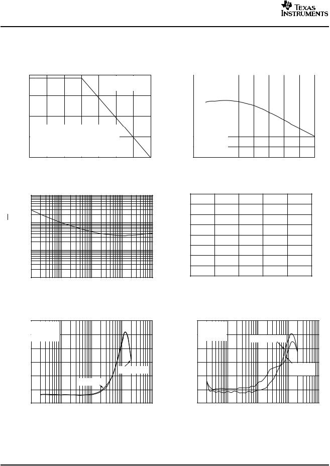
OPA454
www.ti.com
SBOS391–DECEMBER 2007
TYPICAL CHARACTERISTICS (continued)
At TP = +25°C, VS = ±50V, and RL = 4.8kΩ connected to GND, unless otherwise noted.
MAXIMUM POWER DISSIPATION
vs TEMPERATURE WITH MINIMUM ATTACH AREA
|
2.0 |
|
|
|
|
|
|
|
|
|
|
|
|
|
|
|
SO-8 PowerPAD: |
||
|
|
|
|
|
|
|
TJ(max) = +125°C |
||
|
1.5 |
|
|
|
|
|
|
|
|
Dissipation(W) |
1.0 |
|
|
|
|
|
|
|
|
|
TJ (+125°C max) = TA + [(|VS| − |VO|) IO × θJA] |
|
|
||||||
|
0.5 |
θJA = +52°C/W, SO-8 PowerPAD |
|
|
|
|
|||
|
(1in × 0.5in [25.4mm x 12.7mm] |
|
|
|
|
||||
|
|
|
|
|
|
||||
|
|
Heat-Spreader, 1oz Copper) |
|
|
|
|
|||
|
|
TJ = +25°C + (1.93W × 52°C/W) = +125°C |
|
|
|
||||
|
0 |
|
|
|
|
|
|
|
|
|
|
−50 |
−25 |
0 |
25 |
50 |
75 |
100 |
125 |
|
|
|
Exposed Thermal Pad Temperature (°C) |
|
|||||
Figure 26.
INPUT VOLTAGE NOISE SPECTRAL DENSITY
|
1000 |
|
√Hz) |
100 |
|
(nV/ |
||
|
||
VoltageNoise |
10 |
|
|
||
|
1 |
10 |
100 |
1k |
10k |
100k |
Frequency (Hz)
Figure 28.
TOTAL HARMONIC DISTORTION + NOISE vs TEMPERATURE
|
0.040 |
G = +10 |
|
|
|
|
|
|
|
|
|
||
|
0.035 |
RI = 4.75kΩ |
|
|
|
|
|
VPP |
= 38.6V |
|
|
|
|
|
|
|
|
|
||
N(%) |
0.030 |
|
|
|
|
|
0.025 |
|
|
|
|
|
|
+ |
|
|
|
|
|
|
|
|
|
|
|
|
|
THD |
|
|
|
|
VS = −55, +55 |
|
0.020 |
|
|
|
|
|
|
|
|
|
|
|
|
|
|
|
|
|
VS = −49, +50 |
|
|
|
0.015 |
|
|
|
|
|
|
0.010 |
|
|
|
|
|
|
|
10 |
100 |
1k |
10k |
100k |
Frequency (Hz)
Figure 30.
SLEW RATE vs TEMPERATURE
|
16 |
|
|
|
|
|
|
|
|
|
15 |
|
|
|
|
|
|
|
|
µs) |
14 |
|
|
|
|
|
|
||
13 |
|
|
|
|
(V/ |
|
|
|
|
|
|
|
|
|
SlewRate |
12 |
|
|
|
|
|
|
|
|
|
11 |
|
|
|
|
|
|
|
|
|
|
|
|
|
|
10 |
G = +1 |
||
|
VS = ±45V |
|||
|
|
|||
9VIN = 80V Step
RLOAD = 4.8kΩ 8 

−75 −50 −25 |
0 |
25 |
50 |
75 |
100 |
125 |
Exposed Thermal Pad Temperature (°C)
Figure 27.
0.01Hz TO 10Hz INPUT VOLTAGE NOISE
5 V/div
20s/div
Figure 29.
TOTAL HARMONIC DISTORTION + NOISE vs TEMPERATURE
|
0.0030 |
G = +1 |
|
|
|
|
|
|
|
|
|
|
|
||
|
0.0025 |
RI = 4.75kΩ |
|
|
|
|
|
|
VPP |
= 38.6V |
VS |
= +41.6, −40.6 |
|
||
|
|
|
|||||
|
|
|
|
|
|||
N(%) |
0.0020 |
|
|
|
|
|
|
0.0015 |
|
|
|
|
|
|
|
+ |
|
|
|
|
VS = +40.6, |
|
|
|
|
|
|
|
|
||
THD |
|
|
|
|
|
|
|
0.0010 |
|
|
|
|
−39.6 |
|
|
|
|
|
|
|
|
|
|
|
0.0005 |
|
|
|
|
|
|
|
0 |
|
|
|
|
|
|
|
|
10 |
|
100 |
1k |
10k |
100k |
Frequency (Hz)
Figure 31.
10 |
Submit Documentation Feedback |
Copyright © 2007, Texas Instruments Incorporated |
Product Folder Link(s): OPA454

OPA454
www.ti.com
SBOS391–DECEMBER 2007
TYPICAL CHARACTERISTICS (continued)
At TP = +25°C, VS = ±50V, and RL = 4.8kΩ connected to GND, unless otherwise noted.
LARGE-SIGNAL STEP RESPONSE
|
VIN |
|
|
G = +1 |
|
|
TC = +60°C |
|
500mV/div |
CLOAD = 50pF |
|
VCM = +30V |
||
|
||
|
RF = 10kΩ |
|
|
VOUT |
Time (1µs/div)
Figure 32.
LARGE-SIGNAL STEP RESPONSE
(200mV/div) |
(400mV/div) |
|
IN |
OUT |
G = +2 |
V V |
TC = +100°C |
|
|
VIN |
CLOAD = 100pF |
|
VCM = +40V |
|
|
|
|
|
VOUT |
RF = 10kΩ |
Time (2.5µs/div)
Figure 34.
STEP RESPONSE
|
2.0 |
|
|
|
G = +1 |
|
1.5 |
G = +2 |
|
|
|
|
1.0 |
|
(V) |
0.5 |
|
|
|
|
OUT |
0 |
|
|
|
|
V |
−0.5 |
|
|
|
|
|
−1.0 |
|
|
−1.5 |
RF = 10kΩ |
|
CLOAD = 100pF, 125°C |
|
|
−2.0 |
VCM = +40V |
|
|
|
|
|
1µs/div |
Figure 36.
LARGE-SIGNAL STEP RESPONSE
|
VIN |
|
|
G = +1 |
|
|
TC = +105°C |
|
500mV/div |
CLOAD = 50pF |
|
VCM = +30V |
||
|
||
|
RF = 10kΩ |
|
|
VOUT |
Time (1µs/div)
Figure 33.
SMALL-SIGNAL STEP RESPONSE
|
TC = +125°C |
|
TC = +25°C |
50mV |
TC = −55°C |
|
|
|
G = +1 |
|
CLOAD = 100pF |
|
VCM = 0V |
|
RF = 0Ω |
Time (500ns/div)
Figure 35.
|
|
|
|
GAIN PEAKING vs CLOAD |
|
||
|
180 |
|
|
(G = +1, VCM = 0V)(2) |
|
||
|
RF = 0Ω |
|
|
|
|||
|
160 |
|
|
|
|||
|
RF |
= 10kΩ |
TC |
= −55°C |
|
||
|
|
|
|||||
|
140 |
|
|
|
|
||
|
|
|
TC = +25°C |
|
|
||
|
120 |
|
|
|
|
||
Peaking(%) |
|
|
TC = +85°C |
|
|
|
|
100 |
|
|
|
|
|
||
|
|
|
|
|
|
||
TC |
= +125°C |
|
|
|
|||
80 |
|
|
|
|
|
|
|
60 |
|
|
|
|
|
|
|
|
|
|
|
|
|
|
|
|
40 |
|
|
|
|
|
|
|
20 |
|
|
|
|
|
|
|
0 |
|
|
|
|
|
|
|
0 |
|
100 |
200 |
300 |
400 |
500 |
CLOAD (pF)
Figure 37.
(2)See Application section Unity-Gain Noninverting Configuration.
Copyright © 2007, Texas Instruments Incorporated |
Submit Documentation Feedback |
11 |
Product Folder Link(s): OPA454
 Loading...