Texas Instruments MC1488N, SN55188J, SN75188D, SN75188DR, SN75188N Datasheet
...
|
MC1488, SN55188, SN75188 |
||||||
|
QUADRUPLE LINE DRIVERS |
||||||
|
SLLS094B ± SEPTEMBER 1983 ± REVISED MAY 1995 |
||||||
|
|
|
|
|
|
|
|
D Meet or Exceed the Requirements of ANSI |
SN55188 . . . J OR W PACKAGE |
||||||
EIA/TIA-232-E and ITU Recommendation |
MC1488, SN75188 . . . D OR N PACKAGE |
||||||
V.28 |
|
|
(TOP VIEW) |
|
|
||
D Designed to Be Interchangeable With |
VCC ± |
|
|
|
|
VCC + |
|
|
1 |
14 |
|
||||
Motorola MC1488 |
|
|
|||||
|
|
||||||
D Current-Limited Output: 10 mA Typical |
1A |
|
2 |
13 |
|
4B |
|
1Y |
|
3 |
12 |
|
4A |
||
|
|
||||||
D Power-Off Output Impedance: 300 Ω |
|
|
|||||
2A |
|
4 |
11 |
|
4Y |
||
|
|
||||||
Minimum |
2B |
|
5 |
10 |
|
3B |
|
|
|
||||||
D Slew Rate Control by Load Capacitor |
2Y |
|
6 |
9 |
|
3A |
|
|
|
||||||
D Flexible Supply Voltage Range |
GND |
|
7 |
8 |
|
3Y |
|
|
|
||||||
|
|
|
|
|
|||
D Input Compatible With Most TTL Circuits |
|
|
|
|
|
|
|
|
|
|
|
|
|
|
|
description
The MC1488, SN55188, and SN75188 are monolithic quadruple line drivers designed to interface data terminal equipment with data communications equipment in conformance with ANSI EIA/TIA-232-E using a diode in series with each supply-voltage terminal as shown under typical applications.
The SN55188 is characterized for operation over the full military temperature range of ±55°C to 125°C. The MC1488 and SN75188 are characterized for operation from 0°C to 70°C.
SN55188 . . . FK PACKAGE
(TOP VIEW)
|
1A |
CC ± |
NC |
CC+ |
4B |
|
|
V |
V |
|
|||
1Y |
3 |
2 |
1 |
20 19 |
4A |
|
4 |
|
|
|
18 |
||
NC |
5 |
|
|
|
17 |
NC |
2A |
6 |
|
|
|
16 |
4Y |
NC |
7 |
|
|
|
15 |
NC |
2B |
8 |
|
|
|
14 |
3B |
|
9 |
10 11 12 13 |
|
|||
|
2Y |
GND |
NC |
3Y |
3A |
|
FUNCTION TABLE |
NC ± No internal connection |
|||
|
(drivers 2±4) |
|
||
|
|
|
||
|
|
|
|
|
A |
B |
|
Y |
|
|
|
|
|
|
H |
H |
|
L |
|
L |
X |
|
H |
|
X |
L |
|
H |
|
H = high level, L = low level,
X = irrelevant
Please be aware that an important notice concerning availability, standard warranty, and use in critical applications of Texas Instruments semiconductor products and disclaimers thereto appears at the end of this data sheet.
PRODUCTION DATA information is current as of publication date. Products conform to specifications per the terms of Texas Instruments standard warranty. Production processing does not necessarily include testing of all parameters.
Copyright 1995, Texas Instruments Incorporated
POST OFFICE BOX 655303 •DALLAS, TEXAS 75265 |
1 |

MC1488, SN55188, SN75188 QUADRUPLE LINE DRIVERS
SLLS094B ± SEPTEMBER 1983 ± REVISED MAY 1995
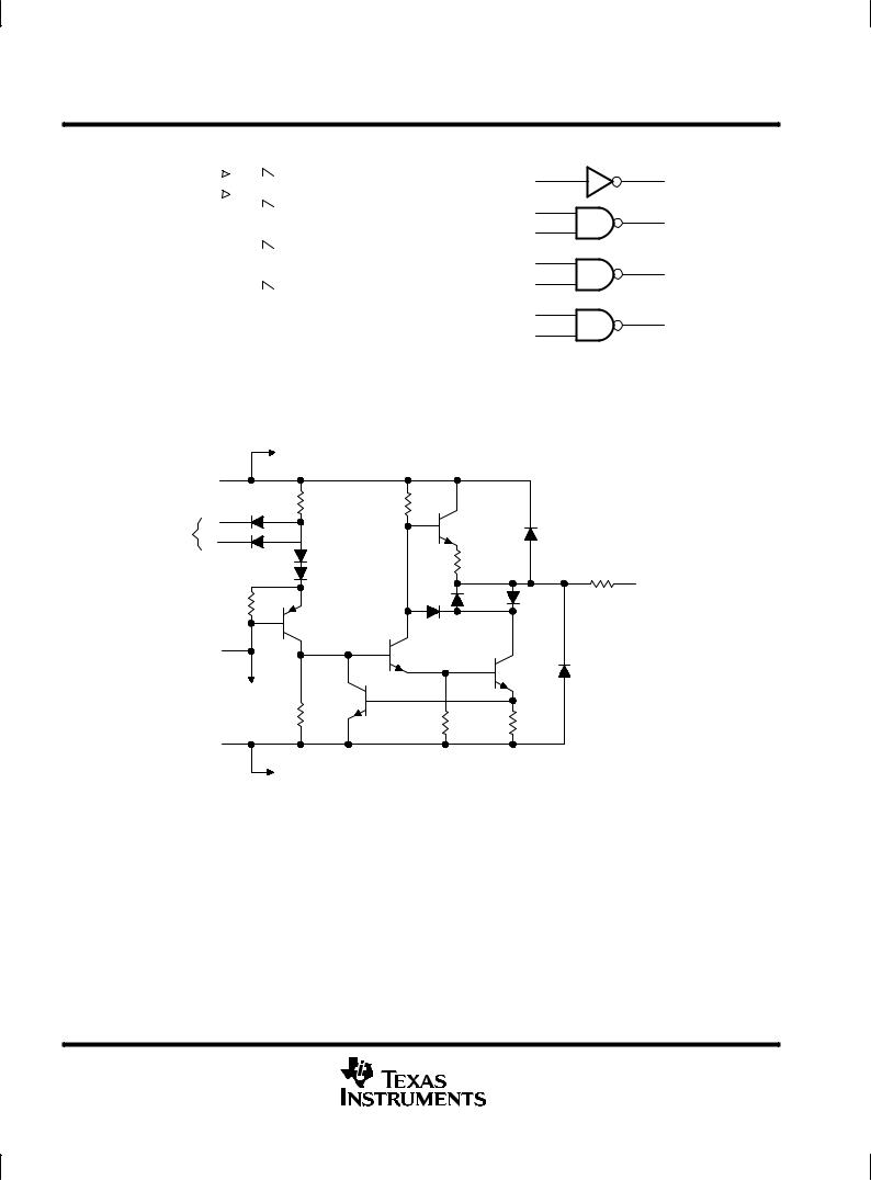
logic symbol²
1A |
2 |
|
3 |
1Y |
|
4 |
|
|
|||
|
|
|
|
||
2A |
& |
6 |
2Y |
||
5 |
|||||
|
|
||||
2B |
|
|
|||
|
|
|
|||
9 |
|
|
|
||
3A |
|
8 |
3Y |
||
|
|||||
10 |
|
||||
|
|
||||
3B |
|
|
|||
|
|
|
|||
12 |
|
|
|
||
4A |
|
11 |
4Y |
||
|
|||||
13 |
|
||||
|
|
||||
4B |
|
|
|||
|
|
|
|||
|
|
|
|
||
|
|
|
|
|
² This symbol is in accordance with ANSI/IEEE Std 91-1984 and IEC Publication 617-12.
Pin numbers shown are for the D and N packages.
logic diagram (positive logic)
1A |
2 |
3 1Y |
||
2A |
4 |
6 |
|
|
|
2Y |
|||
2B |
5 |
|||
|
|
|||
|
|
|
||
3A |
9 |
8 |
|
|
|
3Y |
|||
3B |
10 |
|||
|
|
|||
|
|
|
||
4A |
12 |
11 |
|
|
|
4Y |
|||
4B |
13 |
|||
|
|
|||
|
|
|
||
Positive logic
Y = A (driver 1)
Y = AB or A + B (drivers 2 thru 4)
schematic (each driver)
To Other
Drivers
VCC +
8.2 kΩ |
6.2 kΩ |
A
Input(s)
B
70 Ω
300 Ω
Output
3.6 kΩ
GND
To |
|
|
Other |
|
|
Drivers |
10 kΩ |
70 Ω |
|
3.7 kΩ |
VCC ±
To Other Drivers
Resistor values shown are nominal.
2 |
POST OFFICE BOX 655303 •DALLAS, TEXAS 75265 |

MC1488, SN55188, SN75188
QUADRUPLE LINE DRIVERS
SLLS094B ± SEPTEMBER 1983 ± REVISED MAY 1995
absolute maximum ratings over operating free-air temperature (unless otherwise noted)²
Supply voltage, VCC + at (or below) 25°C free-air temperature (see Notes 1 and 2) . . . . . . . |
. . . . . . . . . . 15 |
V |
|
Supply voltage, VCC ± at (or below) 25°C free-air temperature (see Notes 1 and 2) . . . . . . . . |
. . . . . . . . ±15 V |
||
Input voltage, VI . . . . . . . . . . . . . . . . . . . . . . . . . . . . . . . . . . . . . . . . . . . . . . . . . . . . . . |
. . . . . . . . . . . . |
. . ±15 V to 7 |
V |
Output voltage, VO . . . . . . . . . . . . . . . . . . . . . . . . . . . . . . . . . . . . . . . . . . . . . . . . . . . . |
. . . . . . . . . . . . |
. ±15 V to 15 |
V |
Continuous total power dissipation (see Note 2) . . . . . . . . . . . . . . . . . . . . . . . . . . |
See Dissipation Rating Table |
||
Operating free-air temperature range, TA: SN55188 . . . . . . . . . . . . . . . . . . . . . . |
. . . . . . . . . . . |
±55°C to 125°C |
|
MC1488, SN75188 . . . . . . . . . . . . . |
. . . . . . . . . . . . |
. . 0°C to 70°C |
|
Storage temperature range, Tstg . . . . . . . . . . . . . . . . . . . . . . . . . . . . . . . . . . . . . . . . |
. . . . . . . . . . . |
±65°C to 150°C |
|
Case temperature for 60 seconds, FK package . . . . . . . . . . . . . . . . . . . . . . . . . . . |
. . . . . . . . . . . . |
. . . . . . . 260°C |
|
Lead temperature 1,6 mm (1/16 inch) from case for 10 seconds: D or N package . . . . . . . . . |
. . . . . . . 260°C |
||
Lead temperature 1,6 mm (1/16 inch) from case for 60 seconds: J or W package . . . . . . . . . |
. . . . . . . 300°C |
||
²Stresses beyond those listed under ªabsolute maximum ratingsº may cause permanent damage to the device. These are stress ratings only, and functional operation of the device at these or any other conditions beyond those indicated under ªrecommended operating conditionsº is not implied. Exposure to absolute-maximum-rated conditions for extended periods may affect device reliability.
NOTES: 1. All voltage values are with respect to the network ground terminal.
2.For operation above 25°C free-air temperature, refer to the maximum supply voltage curve, Figure 6. In the FK and J packages, SN55188 chips are alloy mounted.
|
DISSIPATION RATING TABLE |
|
|||
PACKAGE |
TA ≤ 25°C |
DERATING FACTOR |
TA = 70°C |
TA = 125°C |
|
POWER RATING |
ABOVE TA = 25°C |
POWER RATING |
POWER RATING |
||
|
|||||
D |
950 mW |
7.6 mW/°C |
608 mW |
± |
|
FK |
1375 mW |
11.0 mW/°C |
880 mW |
275 mW |
|
J |
1375 mW |
11.0 mW/°C |
880 mW |
275 mW |
|
N |
1150 mW |
9.2 mW/°C |
736 mW |
± |
|
W |
1000 mW |
8.0 mW/°C |
640 mW |
200 mW |
|
|
|
|
|
|
|
recommended operating conditions
|
|
SN55188 |
|
MC1488, SN75188 |
UNIT |
||
|
|
|
|
|
|
|
|
|
MIN |
NOM |
MAX |
MIN |
NOM |
MAX |
|
|
|
||||||
|
|
|
|
|
|
|
|
Supply voltage, VCC + |
7.5 |
9 |
15 |
7.5 |
9 |
15 |
V |
Supply voltage, VCC ± |
± 7.5 |
± 9 |
± 15 |
± 7.5 |
± 9 |
± 15 |
V |
High-level input voltage, VIH |
1.9 |
|
|
1.9 |
|
|
V |
Low-level input voltage, VIL |
|
|
0.8 |
|
|
0.8 |
V |
Operating free-air temperature, TA |
± 55 |
|
125 |
0 |
|
70 |
°C |
POST OFFICE BOX 655303 •DALLAS, TEXAS 75265 |
3 |
 Loading...