


 Loading...
PRODUCT |
SAMPLE & |
TECHNICAL |
TOOLS & |
SUPPORT & |
FOLDER |
BUY |
DOCUMENTS |
SOFTWARE |
COMMUNITY |
LM2734
SNVS288J –SEPTEMBER 2004 –REVISED DECEMBER 2014
LM2734 Thin SOT 1-A Load Step-Down DC-DC Regulator
1 Features
•Thin SOT-6 Package
•3.0-V to 20-V Input Voltage Range
•0.8-V to 18-V Output Voltage Range
•1-A Output Current
•550-kHz (LM2734Y) and 1.6-MHz (LM2734X) Switching Frequencies
•300-mΩ NMOS Switch
•30-nA Shutdown Current
•0.8-V, 2% Internal Voltage Reference
•Internal Soft-Start
•Current-Mode, PWM Operation
•WEBENCH® Online Design Tool
•Thermal Shutdown
•LM2734XQ and LM2734YQ are AEC-Q100 Grade 1 Qualified and are Manufactured on an Automotive Grade Flow.
2 Applications
•Local Point-of-Load Regulation
•Core Power in HDDs
•Set-Top Boxes
•Battery-Powered Devices
•USB Powered Devices
•DSL Modems
•Notebook Computers
•Automotive
|
Typical Application Circuit |
|
||
|
|
|
D2 |
|
VIN |
VIN |
|
BOOST |
|
C1 |
|
|
C3 |
|
|
|
L1 |
|
|
|
|
|
SW |
VOUT |
|
|
|
|
|
ON |
|
LM2734 |
D1 |
|
|
|
C2 |
||
|
|
|
|
|
OFF |
EN |
|
R1 |
|
|
|
|
||
|
|
|
FB |
|
|
|
GND |
R2 |
|
|
|
|
|
|
3 Description
The LM2734 regulator is a monolithic, highfrequency, PWM step-down DC-DC converter in a 6- pin Thin SOT package. The device provides all the active functions to provide local DC-DC conversion with fast transient response and accurate regulation in the smallest possible PCB area.
With a minimum of external components and online design support through WEBENCH, the LM2734 regulator is easy to use. The ability to drive 1-A loads with an internal 300-mΩ NMOS switch using state-of- the-art 0.5-µm BiCMOS technology results in the best power density available. The world-class control circuitry allows for on-times as low as 13 ns, thus supporting exceptionally high-frequency conversion over the entire 3-V to 20-V input operating range down to the minimum output voltage of 0.8 V. Switching frequency is internally set to 550 kHz (LM2734Y) or 1.6 MHz (LM2734X), allowing the use of extremely small surface-mount inductors and chip capacitors. Even though the operating frequencies are very high, efficiencies up to 90% are easy to achieve. External shutdown is included, featuring an ultra-low standby current of 30 nA.
The LM2734 regulator uses current-mode control and internal compensation to provide high-performance regulation over a wide range of operating conditions. Additional features include internal soft-start circuitry to reduce inrush current, pulse-by-pulse current limit, thermal shutdown, and output overvoltage protection.
Device Information(1)
PART NUMBER |
PACKAGE |
BODY SIZE (NOM) |
LM2734 |
SOT (6) |
2.90 mm x 1.60 mm |
(1)For all available packages, see the orderable addendum at the end of the datasheet.
Efficiency vs Load Current
VIN = 5 V, VOUT = 3.3 V
An IMPORTANT NOTICE at the end of this data sheet addresses availability, warranty, changes, use in safety-critical applications, intellectual property matters and other important disclaimers. PRODUCTION DATA.

LM2734
SNVS288J –SEPTEMBER 2004–REVISED DECEMBER 2014 www.ti.com
Table of Contents
1 |
Features .................................................................. |
1 |
|
7.3 |
Feature Description................................................... |
9 |
||
2 |
Applications ........................................................... |
1 |
|
7.4 |
Device Functional Modes........................................ |
10 |
||
3 |
Description ............................................................. |
1 |
8 |
Application and Implementation ........................ |
11 |
|||
4 |
Revision History..................................................... |
2 |
|
8.1 |
Application Information............................................ |
11 |
||
5 |
Pin Configuration and Functions |
3 |
|
8.2 |
Typical Applications ................................................ |
14 |
||
9 |
Power Supply Recommendations |
28 |
||||||
6 |
Specifications |
4 |
||||||
10 |
Layout |
28 |
||||||
|
6.1 |
Absolute Maximum Ratings ...................................... |
4 |
|||||
|
6.2 |
ESD Ratings |
4 |
|
10.1 |
Layout Guidelines ................................................. |
28 |
|
|
|
10.2 |
Layout Example |
29 |
||||
|
6.3 |
Recommended Operating Conditions |
4 |
|
||||
|
11 |
Device and Documentation Support |
30 |
|||||
|
6.4 |
Thermal Information .................................................. |
4 |
|||||
|
6.5 |
Electrical Characteristics........................................... |
5 |
|
11.1 |
Third-Party Products Disclaimer ........................... |
30 |
|
|
6.6 |
Typical Performance Characteristics ........................ |
6 |
|
11.2 |
Trademarks ........................................................... |
30 |
|
7 |
Detailed Description .............................................. |
8 |
|
11.3 |
Electrostatic Discharge Caution............................ |
30 |
||
|
7.1 |
Overview |
8 |
|
11.4 |
Glossary ................................................................ |
30 |
|
|
12 |
Mechanical, Packaging, and Orderable |
|
|||||
|
7.2 |
Functional Block Diagram ......................................... |
9 |
30 |
||||
|
|
|
|
|
Information ........................................................... |
|||
|
|
|
|
|
|
|
|
|
4 Revision History
Changes from Revision I (April 2013) to Revision J Page
•Added ESD Ratings table, Feature Description section, Device Functional Modes, Application and Implementation section, Power Supply Recommendations section, Layout section, Device and Documentation Support section, and
Mechanical, Packaging, and Orderable Information section. ................................................................................................. |
1 |
2 |
Submit Documentation Feedback |
Copyright © 2004–2014, Texas Instruments Incorporated |
Product Folder Links: LM2734

|
|
|
|
|
LM2734 |
www.ti.com |
|
|
|
SNVS288J –SEPTEMBER 2004–REVISED DECEMBER 2014 |
|
5 Pin Configuration and Functions |
|
|
|
|
|
See Package Number DDC (R-PDSO-G6) |
|||||
|
|
6-Lead SOT |
|
|
|
|
|
Top View |
|
|
|
|
|
|
|
|
|
|
|
|
|
|
|
BOOST |
|
1 |
6 |
|
SW |
|
2 |
5 |
|
|
|
GND |
|
|
VIN |
||
|
3 |
4 |
|
|
|
FB |
|
|
EN |
||
|
|
|
|
|
|
|
|
|
|
|
|
|
|
|
|
Pin Functions |
|
PIN |
I/O |
DESCRIPTION |
|
NAME |
|
NO. |
||
|
|
|
||
BOOST |
|
1 |
I |
Boost voltage that drives the internal NMOS control switch. A bootstrap capacitor is |
|
connected between the BOOST and SW pins. |
|||
|
|
|
|
|
GND |
|
2 |
GND |
Signal and Power ground pin. Place the bottom resistor of the feedback network as close as |
|
possible to this pin for accurate regulation. |
|||
|
|
|
|
|
FB |
|
3 |
I |
Feedback pin. Connect FB to the external resistor divider to set output voltage. |
EN |
|
4 |
I |
Enable control input. Logic high enables operation. Do not allow this pin to float or be greater |
|
than VIN + 0.3 V. |
|||
|
|
|
|
|
VIN |
|
5 |
I |
Input supply voltage. Connect a bypass capacitor to this pin. |
SW |
|
6 |
O |
Output switch. Connects to the inductor, catch diode, and bootstrap capacitor. |
Copyright © 2004–2014, Texas Instruments Incorporated |
Submit Documentation Feedback |
3 |
Product Folder Links: LM2734

LM2734
SNVS288J –SEPTEMBER 2004–REVISED DECEMBER 2014 |
www.ti.com |
6 Specifications
6.1 |
Absolute Maximum Ratings |
|
|
|
over operating free-air temperature (unless otherwise noted)(1)(2) |
|
|
|
|
|
|
MIN |
MAX |
UNIT |
VIN |
|
-0.5 |
24 |
V |
SW Voltage |
-0.5 |
24 |
V |
|
Boost Voltage |
-0.5 |
30 |
V |
|
Boost to SW Voltage |
-0.5 |
6.0 |
V |
|
FB Voltage |
-0.5 |
0.3 |
V |
|
EN Voltage |
-0.5 |
VIN + 0.3 |
V |
|
Junction Temperature |
|
150 |
°C |
|
Soldering Information Reflow Peak Pkg. Temp.(15s) |
|
260 |
°C |
|
Tstg |
Storage temperature |
-65 |
150 |
°C |
(1)Stresses beyond those listed under Absolute Maximum Ratings may cause permanent damage to the device. These are stress ratings only, which do not imply functional operation of the device at these or any other conditions beyond those indicated under Recommended Operating Conditions. Exposure to absolute-maximum-rated conditions for extended periods may affect device reliability.
(2)If Military/Aerospace specified devices are required, please contact the Texas Instruments Sales Office/ Distributors for availability and specifications.
6.2 |
ESD Ratings |
|
|
|
|
|
|
|
|
|
|
|
|
VALUE |
UNIT |
V |
Electrostatic discharge |
Human Body Model (HBM), per ANSI/ESDA/JEDEC JS001(1) |
|
|
±2000 |
V |
|
ESD |
|
|
|
|
|
|
|
(1) JEDEC document JEP155 states that 500-V HBM allows safe manufacturing with a standard ESD control process. |
|
|
|||||
6.3 |
Recommended Operating Conditions |
|
|
|
|
||
over operating free-air temperature range (unless otherwise noted) |
|
|
|
|
|||
|
|
|
MIN |
NOM |
MAX |
UNIT |
|
VIN |
|
|
3 |
|
|
20 |
V |
SW Voltage |
|
-0.5 |
|
|
20 |
V |
|
Boost Voltage |
|
-0.5 |
|
|
25 |
V |
|
Boost to SW Voltage |
|
1.6 |
|
|
5.5 |
V |
|
Junction Temperature Range |
|
−40 |
|
|
125 |
°C |
|
6.4 Thermal Information
|
|
LM2734 |
|
|
|
THERMAL METRIC(1) |
DDC |
UNIT |
|
|
|
6 PINS |
|
|
RθJA |
Junction-to-ambient thermal resistance |
158.1 |
|
|
RθJC(top) |
Junction-to-case (top) thermal resistance |
46.5 |
|
|
RθJB |
Junction-to-board thermal resistance |
29.5 |
°C/W |
|
ψJT |
Junction-to-top characterization parameter |
0.8 |
||
|
||||
ψJB |
Junction-to-board characterization parameter |
29.2 |
|
|
RθJC(bot) |
Junction-to-case (bottom) thermal resistance |
n/a |
|
(1)For more information about traditional and new thermal metrics, see the IC Package Thermal Metrics application report, SPRA953.
4 |
Submit Documentation Feedback |
Copyright © 2004–2014, Texas Instruments Incorporated |
Product Folder Links: LM2734

LM2734
www.ti.com |
SNVS288J –SEPTEMBER 2004–REVISED DECEMBER 2014 |
6.5 Electrical Characteristics
VIN = 5V, VBOOST - VSW = 5V unless otherwise specified. Datasheet min/max specification limits are ensured by design, test, or statistical analysis.
|
PARAMETER |
TEST CONDITIONS |
|
TJ = 25°C |
|
TJ = -40°C to 125°C |
|
UNIT |
||
|
MIN(1) |
TYP(2) |
MAX(1) |
MIN |
TYP |
MAX |
||||
|
|
|
|
|||||||
VFB |
Feedback Voltage |
|
|
0.800 |
|
|
0.784 |
|
0.816 |
V |
VFB/ |
Feedback Voltage Line |
VIN = 3V to 20V |
|
0.01 |
|
|
|
|
|
% / V |
VIN |
Regulation |
|
|
|
|
|
|
|
|
|
IFB |
Feedback Input Bias |
Sink/Source |
|
10 |
|
|
|
|
250 |
nA |
Current |
|
|
|
|
|
|
||||
|
Undervoltage Lockout |
VIN Rising |
|
2.74 |
|
|
|
|
2.90 |
|
UVLO |
Undervoltage Lockout |
VIN Falling |
|
2.3 |
|
|
2.0 |
|
|
V |
|
UVLO Hysteresis |
|
|
0.44 |
|
|
0.30 |
|
0.62 |
|
FSW |
Switching Frequency |
LM2734X |
|
1.6 |
|
|
1.2 |
|
1.9 |
MHz |
LM2734Y |
|
0.55 |
|
|
0.40 |
|
0.66 |
|||
|
|
|
|
|
|
|
||||
DMAX |
Maximum Duty Cycle |
LM2734X |
|
92 |
|
|
85% |
|
|
|
LM2734Y |
|
96 |
|
|
90% |
|
|
|
||
|
|
|
|
|
|
|
|
|||
DMIN |
Minimum Duty Cycle |
LM2734X |
|
2% |
|
|
|
|
|
|
LM2734Y |
|
1% |
|
|
|
|
|
|
||
|
|
|
|
|
|
|
|
|
||
RDS(ON) |
Switch ON Resistance |
VBOOST - VSW = 3V |
|
300 |
|
|
|
|
600 |
mΩ |
ICL |
Switch Current Limit |
VBOOST - VSW = 3V |
|
1.7 |
|
|
1.2 |
|
2.5 |
A |
IQ |
Quiescent Current |
Switching |
|
1.5 |
|
|
|
|
2.5 |
mA |
|
Quiescent Current |
VEN = 0V |
|
30 |
|
|
|
|
|
nA |
|
(shutdown) |
|
|
|
|
|
|
|
|
|
|
|
LM2734X (50% Duty |
|
2.5 |
|
|
|
|
3.5 |
|
|
|
Cycle) |
|
|
|
|
|
|
||
IBOOST |
Boost Pin Current |
|
|
|
|
|
|
|
mA |
|
LM2734Y (50% Duty |
|
1.0 |
|
|
|
|
1.8 |
|||
|
|
Cycle) |
|
|
|
|
|
|
||
|
|
|
|
|
|
|
|
|
|
|
|
Shutdown Threshold |
VEN Falling |
|
|
|
|
|
|
0.4 |
|
|
Voltage |
|
|
|
|
|
|
|
|
|
VEN_TH |
|
|
|
|
|
|
|
|
V |
|
Enable Threshold |
VEN Rising |
|
|
|
|
1.8 |
|
|
||
|
Voltage |
|
|
|
|
|
|
|
|
|
IEN |
Enable Pin Current |
Sink/Source |
|
10 |
|
|
|
|
|
nA |
ISW |
Switch Leakage |
|
|
40 |
|
|
|
|
|
nA |
(1)Specified to Average Outgoing Quality Level (AOQL).
(2)Typicals represent the most likely parametric norm.
Copyright © 2004–2014, Texas Instruments Incorporated |
Submit Documentation Feedback |
5 |
Product Folder Links: LM2734

LM2734
SNVS288J –SEPTEMBER 2004–REVISED DECEMBER 2014 |
www.ti.com |
6.6 Typical Performance Characteristics
All curves taken at VIN = 5 V, VBOOST - VSW = 5 V and TA = 25°C, unless specified otherwise.
|
Figure 1. Oscillator Frequency vs Temperature - L1 = 4.7 µH |
Figure 2. Oscillator Frequency vs Temperature - L1 = 10 μH |
|
|
|
|
Figure 3. Current Limit vs Temperature |
Figure 4. Current Limit vs Temperature |
|
|
VIN = 20 V |
|
Figure 5. VFB vs Temperature |
Figure 6. RDSON vs Temperature |
|
|
|
6 |
Submit Documentation Feedback |
Copyright © 2004–2014, Texas Instruments Incorporated |
|
Product Folder Links: LM2734 |
|
LM2734
www.ti.com |
SNVS288J –SEPTEMBER 2004–REVISED DECEMBER 2014 |
Typical Performance Characteristics (continued)
All curves taken at VIN = 5 V, VBOOST - VSW = 5 V and TA = 25°C, unless specified otherwise.
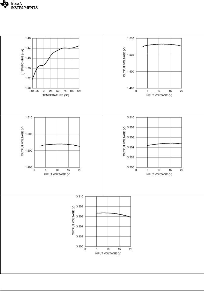
Figure 7. IQ Switching vs Temperature |
Figure 8. Line Regulation - L1 = 4.7 µH |
|
VOUT = 1.5 V, IOUT = 500 mA |
Figure 9. Line Regulation - L1 = 10 μH |
Figure 10. Line Regulation - L1 = 4.7 µH |
VOUT = 1.5 V, IOUT = 500 mA |
VOUT = 3.3 V, IOUT = 500 mA |
Figure 11. Line Regulation - L1 = 10 μH
VOUT = 3.3 V, IOUT = 500 mA
Copyright © 2004–2014, Texas Instruments Incorporated |
Submit Documentation Feedback |
7 |
Product Folder Links: LM2734
LM2734
SNVS288J –SEPTEMBER 2004–REVISED DECEMBER 2014 |
www.ti.com |
7 Detailed Description
7.1 Overview
The LM2734 device is a constant frequency PWM buck regulator IC that delivers a 1-A load current. The regulator has a preset switching frequency of either 550 kHz (LM2734Y) or 1.6 MHz (LM2734X). These high frequencies allow the LM2734 device to operate with small surface-mount capacitors and inductors, resulting in DC-DC converters that require a minimum amount of board space. The LM2734 device is internally compensated, so it is simple to use, and requires few external components. The LM2734 device uses currentmode control to regulate the output voltage.
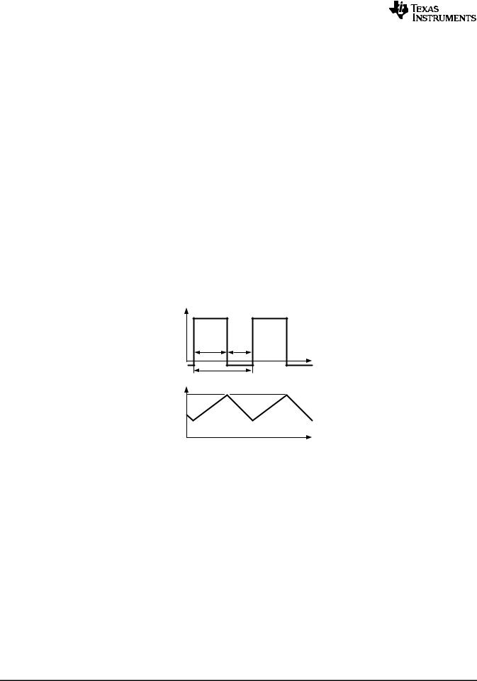
The following operating description of the LM2734 device will refer to the Simplified Block Diagram () and to the waveforms in Figure 12. The LM2734 device supplies a regulated output voltage by switching the internal NMOS control switch at constant frequency and variable duty cycle. A switching cycle begins at the falling edge of the reset pulse generated by the internal oscillator. When this pulse goes low, the output control logic turns on the internal NMOS control switch. During this on-time, the SW pin voltage (VSW) swings up to approximately VIN, and the inductor current (IL) increases with a linear slope. IL is measured by the current-sense amplifier, which generates an output proportional to the switch current. The sense signal is summed with the regulator’s corrective ramp and compared to the error amplifier’s output, which is proportional to the difference between the feedback voltage and VREF. When the PWM comparator output goes high, the output switch turns off until the next switching cycle begins. During the switch off-time, inductor current discharges through Schottky diode D1, which forces the SW pin to swing below ground by the forward voltage (VD) of the catch diode. The regulator loop adjusts the duty cycle (D) to maintain a constant output voltage.
VSW
D = TON/TSW
VIN
SW |
|
|
Voltage |
TOFF |
|
TON |
||
0 |
t |
|
VD |
||
|
||
IL |
TSW |
|
|
||
IPK |
|
|
Inductor |
|
|
Current |
|
|
0 |
t |
Figure 12. LM2734 Waveforms of SW Pin Voltage and Inductor Current
8 |
Submit Documentation Feedback |
Copyright © 2004–2014, Texas Instruments Incorporated |
Product Folder Links: LM2734
LM2734
www.ti.com |
SNVS288J –SEPTEMBER 2004–REVISED DECEMBER 2014 |
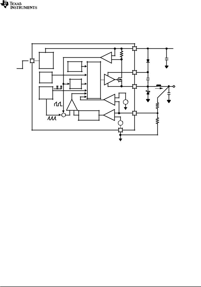
7.2 Functional Block Diagram
ON EN |
OFF
Internal
Regulator
and
Enable
Circuit
Under
Voltage
Lockout
Oscillator |
Reset |
|
Pulse |
|
ISENSE |
|
+ |
|
+ |
Corrective Ramp
VIN
 VIN
VIN
Current-Sense Amplifier
+RSENSE
|
|
- |
|
|
D2 |
CIN |
|
|
|
|
|
|
|
Thermal |
|
|
|
|
|
|
Shutdown |
|
|
|
BOOST |
|
|
|
|
|
|
|
VBOOST |
|
|
Output |
Driver |
0.3: |
|
CBOOST |
|
Current |
Control |
|
Switch |
SW |
VSW L |
|
Limit |
Logic |
|
|
|
|
VOUT |
|
|
OVP |
|
|
|
|
|
|
|
|
D |
IL |
|
|
|
Comparator |
|
|
||
|
|
|
|
|
1 |
COUT |
|
|
|
- |
|
0.88V |
|
|
|
PWM |
+ |
|
+ |
|
|
|
|
|
- |
R |
|
+ |
- |
Comparator |
|
|
|
1 |
|
|
|
|
FB |
||
|
|
|
|
|
||
|
|
|
|
|
|
|
|
|
Internal |
- |
|
|
|
Error |
Compensation |
+ |
|
|
R |
|
|
|
|
|
|||
Signal |
|
|
+ VREF |
|||
Error Amplifier |
2 |
|||||
|
|
- |
0.8V |
|
||
|
|
|
|
|
|
|
GND
7.3 Feature Description
7.3.1 Output Overvoltage Protection
The overvoltage comparator compares the FB pin voltage to a voltage that is 10% higher than the internal reference Vref. Once the FB pin voltage goes 10% above the internal reference, the internal NMOS control switch is turned off, which allows the output voltage to decrease toward regulation.
7.3.2 Undervoltage Lockout
Undervoltage lockout (UVLO) prevents the LM2734 from operating until the input voltage exceeds 2.74 V (typical).
The UVLO threshold has approximately 440 mV of hysteresis, so the part will operate until VIN drops below 2.3 V (typical). Hysteresis prevents the part from turning off during power up if VIN is nonmonotonic.
7.3.3 Current Limit
The LM2734 device uses cycle-by-cycle current limiting to protect the output switch. During each switching cycle, a current limit comparator detects if the output switch current exceeds 1.7 A (typical), and turns off the switch until the next switching cycle begins.
7.3.4 Thermal Shutdown
Thermal shutdown limits total power dissipation by turning off the output switch when the IC junction temperature exceeds 165°C. After thermal shutdown occurs, the output switch does not turn on until the junction temperature drops to approximately 150°C.
Copyright © 2004–2014, Texas Instruments Incorporated |
Submit Documentation Feedback |
9 |
Product Folder Links: LM2734

LM2734
SNVS288J –SEPTEMBER 2004–REVISED DECEMBER 2014 |
www.ti.com |
7.4 Device Functional Modes
7.4.1 Enable Pin / Shutdown Mode
The LM2734 device has a shutdown mode that is controlled by the enable pin (EN). When a logic low voltage is applied to EN, the part is in shutdown mode and its quiescent current drops to typically 30 nA. Switch leakage adds another 40 nA from the input supply. The voltage at this pin should never exceed VIN + 0.3 V.
7.4.2 Soft-Start
This function forces VOUT to increase at a controlled rate during start up. During soft-start, the error amplifier’s reference voltage ramps from 0 V to its nominal value of 0.8 V in approximately 200 µs. This forces the regulator output to ramp up in a more linear and controlled fashion, which helps reduce inrush current. Under some circumstances at start-up, an output voltage overshoot may still be observed. This may be due to a large output load applied during start up. Large amounts of output external capacitance can also increase output voltage overshoot. A simple solution is to add a feed forward capacitor with a value between 470 pf and 1000 pf across the top feedback resistor (R1). See Figure 23 for further detail.
10 |
Submit Documentation Feedback |
Copyright © 2004–2014, Texas Instruments Incorporated |
Product Folder Links: LM2734
LM2734
www.ti.com |
SNVS288J –SEPTEMBER 2004–REVISED DECEMBER 2014 |
8 Application and Implementation
NOTE
Information in the following applications sections is not part of the TI component specification, and TI does not warrant its accuracy or completeness. TI’s customers are responsible for determining suitability of components for their purposes. Customers should validate and test their design implementation to confirm system functionality.
8.1 Application Information
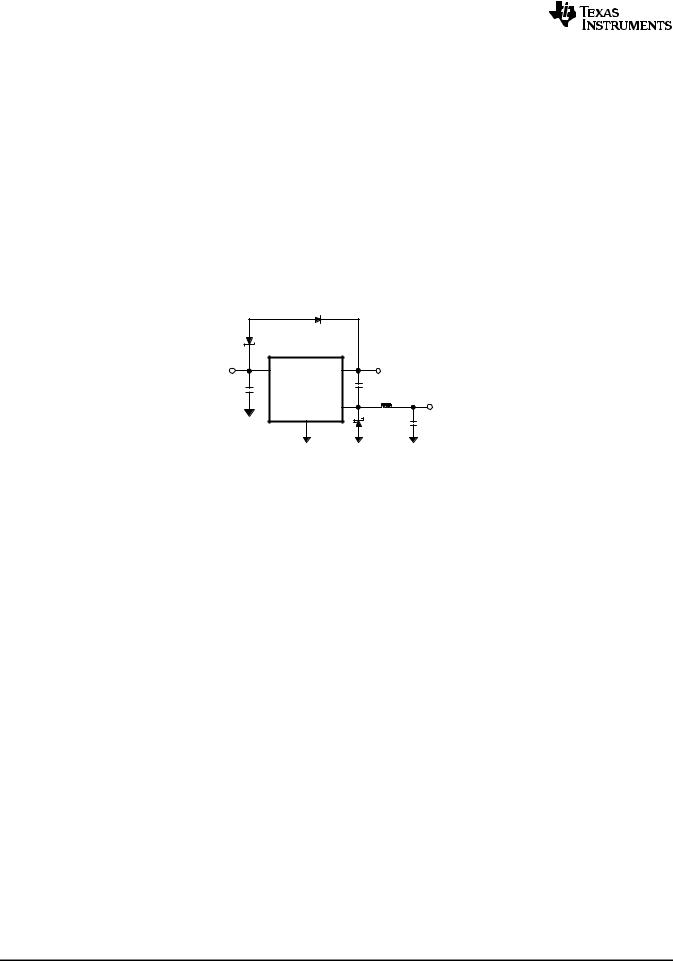
8.1.1 Boost Function
Capacitor CBOOST and diode D2 in Figure 13 are used to generate a voltage VBOOST. VBOOST - VSW is the gate drive voltage to the internal NMOS control switch. To properly drive the internal NMOS switch during its on-time,
VBOOST needs to be at least 1.6 V greater than VSW. Although the LM2734 device will operate with this minimum voltage, it may not have sufficient gate drive to supply large values of output current. Therefore, it is
recommended that VBOOST be greater than 2.5 V above VSW for best efficiency. VBOOST – VSW should not exceed the maximum operating limit of 5.5 V.
5.5 V > VBOOST – VSW > 2.5 V for best performance.
|
|
|
VBOOST |
|
|
|
D2 |
VIN |
VIN |
BOOST |
|
CIN |
|
LM2734 |
CBOOST |
L
SW 
 VOUT
VOUT
GND
D1 |
|
|
|
|
COUT |
|
|
||||
|
|
|
|
|
|
Figure 13. VOUT Charges CBOOST
When the LM2734 device starts up, internal circuitry from the BOOST pin supplies a maximum of 20 mA to
CBOOST. This current charges CBOOST to a voltage sufficient to turn the switch on. The BOOST pin will continue to source current to CBOOST until the voltage at the feedback pin is greater than 0.76 V.
There are various methods to derive VBOOST:
1.From the input voltage (VIN)
2.From the output voltage (VOUT)
3.From an external distributed voltage rail (VEXT)
4.From a shunt or series Zener diode
In the simplified block diagram of Functional Block Diagram, capacitor CBOOST and diode D2 supply the gatedrive current for the NMOS switch. Capacitor CBOOST is charged via diode D2 by VIN. During a normal switching cycle, when the internal NMOS control switch is off (TOFF) (refer to Figure 12), VBOOST equals VIN minus the forward voltage of D2 (VFD2), during which the current in the inductor (L) forward biases the Schottky diode D1
(VFD1). Therefore the voltage stored across CBOOST is:
VBOOST - VSW = VIN - VFD2 + VFD1 |
(1) |
When the NMOS switch turns on (TON), the switch pin rises to:
VSW = VIN – (RDSON × IL), |
(2) |
forcing VBOOST to rise thus reverse biasing D2. The voltage at VBOOST is then:
VBOOST = 2VIN – (RDSON × IL) – VFD2 + VFD1 |
(3) |
which is approximately:
2VIN - 0.4 V |
|
(4) |
|
|
|
Copyright © 2004–2014, Texas Instruments Incorporated |
Submit Documentation Feedback |
11 |
|
Product Folder Links: LM2734 |
|
LM2734
SNVS288J –SEPTEMBER 2004–REVISED DECEMBER 2014 |
www.ti.com |
Application Information (continued)
for many applications. Thus the gate-drive voltage of the NMOS switch is approximately:
VIN - 0.2 V |
(5) |
An alternate method for charging CBOOST is to connect D2 to the output as shown in Figure 13. The output voltage should be from 2.5 V and 5.5 V, so that proper gate voltage will be applied to the internal switch. In this
circuit, CBOOST provides a gate drive voltage that is slightly less than VOUT.
In applications where both VIN and VOUT are greater than 5.5 V, or less than 3 V, CBOOST cannot be charged directly from these voltages. If VIN to VOUT are greater than 5.5 V, CBOOST can be charged from VIN or VOUT minus a Zener voltage by placing a Zener diode D3 in series with D2, as shown in Figure 14. When using a series
Zener diode from the input, ensure that the regulation of the input supply does not create a voltage that falls outside the recommended VBOOST voltage.
(VINMAX – VD3) < 5.5 V |
|
|
|
(6) |
(VINMIN – VD3) > 1.6 V |
|
|
|
(7) |
|
|
D2 |
|
|
D3 |
|
|
|
|
VIN |
VIN |
BOOST |
VBOOST |
|
CIN |
|
LM2734 |
CBOOST |
|
|
|
SW |
L |
VOUT |
|
|
|
||
|
|
GND |
D1 |
COUT |
|
|
|
Figure 14. Zener Reduces Boost Voltage from VIN
An alternative method is to place the Zener diode D3 in a shunt configuration as shown in Figure 15. A small 350 mW to 500 mW 5.1-V Zener diode in a SOT or SOD package can be used for this purpose. A small ceramic capacitor such as a 6.3 V, 0.1-µF capacitor (C4) should be placed in parallel with the Zener diode. When the internal NMOS switch turns on, a pulse of current is drawn to charge the internal NMOS gate capacitance. The 0.1-µF parallel shunt capacitor ensures that the VBOOST voltage is maintained during this time.
Resistor R3 should be chosen to provide enough RMS current to the Zener diode (D3) and to the BOOST pin. A
recommended choice for the Zener current (IZENER) is 1 mA. The current IBOOST into the BOOST pin supplies the gate current of the NMOS control switch and varies typically according to the following formula for the X version:
IBOOST = 0.56 × (D + 0.54) × (VZENER – VD2) mA |
(8) |
IBOOST can be calculated for the Y version using the following:
IBOOST = 0.22 × (D + 0.54) × (VZENER - VD2) µA |
(9) |
where D is the duty cycle, VZENER and VD2 are in volts, and IBOOST is in milliamps. VZENER is the voltage applied to the anode of the boost diode (D2), and VD2 is the average forward voltage across D2. Note that this formula for
IBOOST gives typical current. For the worst case IBOOST, increase the current by 40%. In that case, the worst case boost current will be:
IBOOST-MAX = 1.4 × IBOOST |
(10) |
R3 will then be given by:
R3 = (VIN - VZENER) / (1.4 × IBOOST + IZENER) |
(11) |
For example, using the X-version let VIN = 10 V, VZENER = 5 V, VD2 = 0.7 V, IZENER = 1 mA, and duty cycle D = 50%. Then:
IBOOST = 0.56 × (0.5 + 0.54) × (5 - 0.7) mA = 2.5 mA |
(12) |
R3 = (10 V - 5 V) / (1.4 × 2.5 mA + 1 mA) = 1.11 kΩ |
(13) |
12 |
Submit Documentation Feedback |
Copyright © 2004–2014, Texas Instruments Incorporated |
Product Folder Links: LM2734
Loading...