

SLAU319S–July 2010–Revised April 2018
MSP430™ Flash Device Bootloader (BSL)
The MSP430™ bootloader (BSL) (formerly known as the bootstrap loader) allows users to communicate
with embedded memory in the MSP430 microcontroller (MCU) during the prototyping phase, final
production, and in service. Both the programmable memory (flash memory) and the data memory (RAM)
can be modified as required. Do not confuse the bootloader with the bootstrap loader programs found in
some digital signal processors (DSPs) that automatically load program code (and data) from external
memory to the internal memory of the DSP.
To use the bootloader, a specific BSL entry sequence must be applied. An added sequence of commands
initiates the desired function. A bootloading session can be exited by continuing operation at a defined
user program address or by the reset condition.
If the device is secured by disabling JTAG, it is still possible to use the BSL. Access to the MSP430 MCU
memory through the BSL is protected against misuse by the BSL password. The BSL password is equal
to the content of Interrupt Vector table on the device.
Contents
1 Introduction ................................................................................................................... 3
1.1 Supplementary Online Information ............................................................................... 3
1.2 Overview of BSL Features......................................................................................... 4
1.3 Standard RESET and BSL Entry Sequence .................................................................... 5
1.4 UART Protocol ...................................................................................................... 6
1.5 USB Protocol........................................................................................................ 7
2 Bootloader Protocol – 1xx, 2xx, and 4xx Families....................................................................... 8
2.1 Synchronization Sequence ........................................................................................ 8
2.2 Commands .......................................................................................................... 8
2.3 Programming Flow.................................................................................................. 8
2.4 Data Frame.......................................................................................................... 9
2.5 Loadable BSL...................................................................................................... 14
2.6 Exiting the BSL .................................................................................................... 15
2.7 Password Protection.............................................................................................. 15
2.8 Code Protection Fuse............................................................................................. 15
2.9 BSL Internal Settings and Resources .......................................................................... 16
3 Bootloader Protocol – F5xx and F6xx Families ........................................................................ 19
3.1 BSL Data Packet .................................................................................................. 19
3.2 UART Peripheral Interface (PI).................................................................................. 19
3.3 I
3.4 USB Peripheral Interface......................................................................................... 22
3.5 BSL Core Command Structure .................................................................................. 22
3.6 BSL Security ....................................................................................................... 24
3.7 BSL Core Responses............................................................................................. 25
3.8 BSL Public Functions and Z-Area............................................................................... 27
4 Bootloader Hardware ...................................................................................................... 29
4.1 Hardware Description............................................................................................. 29
5 Differences Between Devices and Bootloader Versions.............................................................. 33
5.1 1xx, 2xx, and 4xx BSL Versions................................................................................. 33
5.2 Special Consideration for ROM BSL Version 1.10 ........................................................... 40
5.3 1xx, 2xx, and 4xx BSL Known Issues .......................................................................... 41
5.4 Special Note on the MSP430F14x Device Family BSL ...................................................... 41
2
C Peripheral Interface........................................................................................... 20
User's Guide
SLAU319S–July 2010–Revised April 2018
Submit Documentation Feedback
MSP430™ Flash Device Bootloader (BSL)
Copyright © 2010–2018, Texas Instruments Incorporated
1

6 Bootloader PCB Layout Suggestion ..................................................................................... 48
1 Standard RESET Sequence ............................................................................................... 5
2 BSL Entry Sequence at Shared JTAG Pins.............................................................................. 5
3 BSL Entry Sequence at Dedicated JTAG Pins .......................................................................... 6
4 Basic Protocol - Byte Level ACK......................................................................................... 20
5 Byte Level ACK............................................................................................................. 21
6 Bootloader Interface Schematic.......................................................................................... 29
7 Universal BSL Interface PCB Layout, Top.............................................................................. 48
8 Universal BSL Interface PCB Layout, Bottom.......................................................................... 48
9 Universal BSL Interface Component Placement....................................................................... 49
10 Universal BSL Interface Component Placement....................................................................... 50
Trademarks
MSP430, E2E are trademarks of Texas Instruments.
All other trademarks are the property of their respective owners.
www.ti.com
5.5 F5xx and F6xx Flash-Based BSL Versions.................................................................... 42
List of Figures
2
MSP430™ Flash Device Bootloader (BSL)
Copyright © 2010–2018, Texas Instruments Incorporated
SLAU319S–July 2010–Revised April 2018
Submit Documentation Feedback

www.ti.com
1 Introduction
The bootloader provides a method to program the flash memory during MSP430 project development and
updates. It can be activated by a utility that sends commands using the UART protocol. The BSL enables
the user to control the activity of the MSP430 MCU and to exchange data using a personal computer or
other device.
To avoid accidental overwriting of the BSL code, this code is stored in a secure memory location, either
ROM or specially protected flash. To prevent unwanted source readout, any BSL command that directly or
indirectly allows data reading is password protected.
To invoke the bootloader, a BSL entry sequence must be applied to dedicated pins. After that, a
synchronization character, followed by the data frame of a specific command, initiates the desired
function.
1.1 Supplementary Online Information
As a compliment to this document, visit Bootloader (BSL) for MSP low-power microcontrollers. This page
contains links to additional BSL user's guides, source code, firmware images, and the BSL scripter with
documentation and code examples.
Additional support is provided by the TI E2E™ Community.
Introduction
SLAU319S–July 2010–Revised April 2018
Submit Documentation Feedback
MSP430™ Flash Device Bootloader (BSL)
Copyright © 2010–2018, Texas Instruments Incorporated
3
Introduction
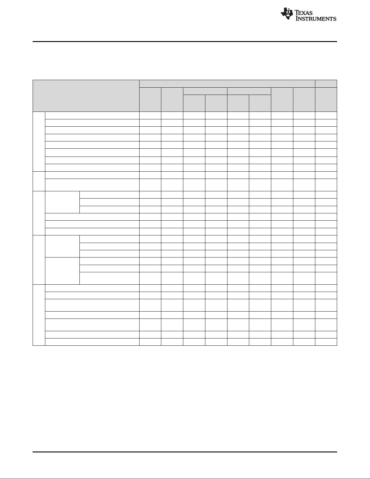
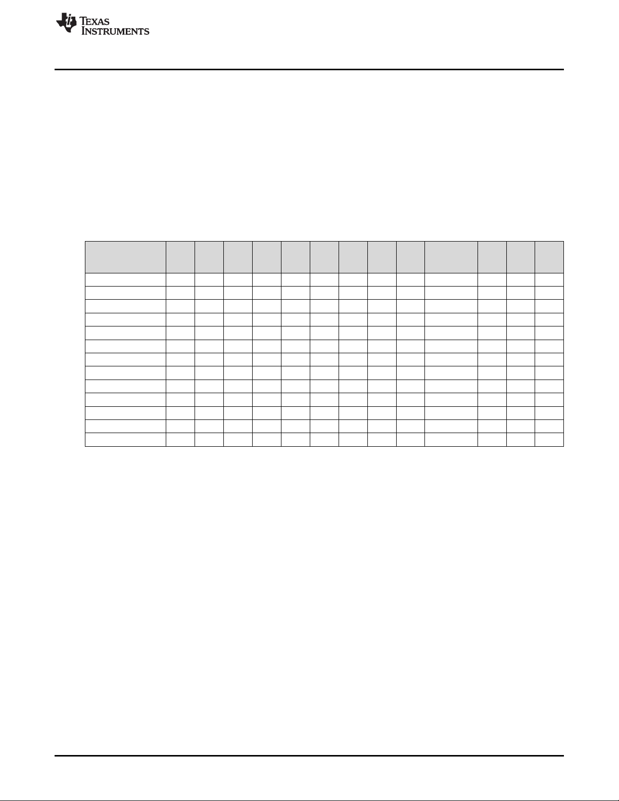
1.2 Overview of BSL Features
Table 1 summarizes the BSL features of the MSP devices, organized by device family.
Table 1. BSL Overview
MSP430 MSP432
G2xx0,
G2xx1,
G2xx2,
I20xx
F1xx,
F2xx,
F4xx,
G2xx3
BSL memory type No BSL ROM Flash
BSL memory size N/A 1 KB 2 KB 2 KB 2 KB 4 KB 3 KB 1 KB 8 KB
Peripheral configured by TLV ✔ ✔ ✔
User configuration ✔
UART ✔ ✔ ✔ ✔ ✔ ✔ ✔
General
I2C
SPI ✔
USB ✔
'1xx, 2xx, 4xx' protocol ✔
'5xx, 6xx' protocol ✔ ✔ ✔ ✔ ✔ ✔ ✔
Protocol
Sequence on TEST/RST ✔ ✔ ✔ ✔ ✔ ✔
Entry sequence
on I/Os
PUR pin tied to V
USB
Sequence on defined I/O ✔ ✔
Empty reset vector invokes BSL ✔ ✔ ✔ ✔
Calling BSL from software application ✔ ✔ ✔ ✔ ✔ ✔ ✔ ✔
Invoke mechanism
Invalid or incomplete application ✔
MSP-BSL 'Rocket' ✔ ✔ ✔ ✔ ✔ ✔ ✔
Hardware
MSP-FET ✔ ✔ ✔ ✔ ✔ ✔ ✔
USB cable ✔
BSL Scripter ✔ ✔ ✔ ✔ ✔ ✔ ✔
BSLDEMO ✔
(1)
Software
Tools Support
MSPBSL library ✔
Password protection 32 byte 32 byte
Mass erase on incorrect password
(5)
✔ ✔ ✔ ✔ ✔ ✔ ✔
Completely disable the BSL using signature or
erasing the BSL
BSL payload encryption ✔ ✔
Security
Update of IP protected regions through boot
code
Authenticated encryption ✔
Additional security ✔
F5xx, F6xx FR5xx, FR6xx
NonUSB
USB Factory
(2)
Flash
(1)
FR2x33,
FR231x
Crypto-
Boot-
loader
(2)
ROM FRAM ROM ROM Flash
FR413x,
FR211x
✔ ✔ ✔ ✔ ✔
✔
UART
only
(4)
32 byte 32 byte 32 byte 32 byte 256 byte
UART
✔
only
✔ ✔ ✔ ✔ ✔ ✔ ✔
(7)
www.ti.com
P401R
(2)
(3)
✔
(6)
✔
(1)
All BSL software collateral (application, examples, source code, and firmware images) is available in the BSL tool folder.
The MSP430 USB developers package includes additional USB BSL sample applications.
(2)
BSL in flash memory allows to replace the BSL with a custom version.
(3)
MSP-FET supports UART and I2C BSL communication only.
(4)
F543x (non A) has a 16-byte password.
(5)
Some devices can disable mass erase on incorrect password. See the device family user's guide.
(6)
The decryption of the payload is performed by the device bootcode.
(7)
Firmware validation through CRC.
4
MSP430™ Flash Device Bootloader (BSL)
Copyright © 2010–2018, Texas Instruments Incorporated
SLAU319S–July 2010–Revised April 2018
Submit Documentation Feedback
Bootloader Starts
RST DTR/NMI ( )
TEST ( )RTS
t
SBW,en
RST DTR/NMI ( )
TEST ( )RTS
User Program Starts
www.ti.com
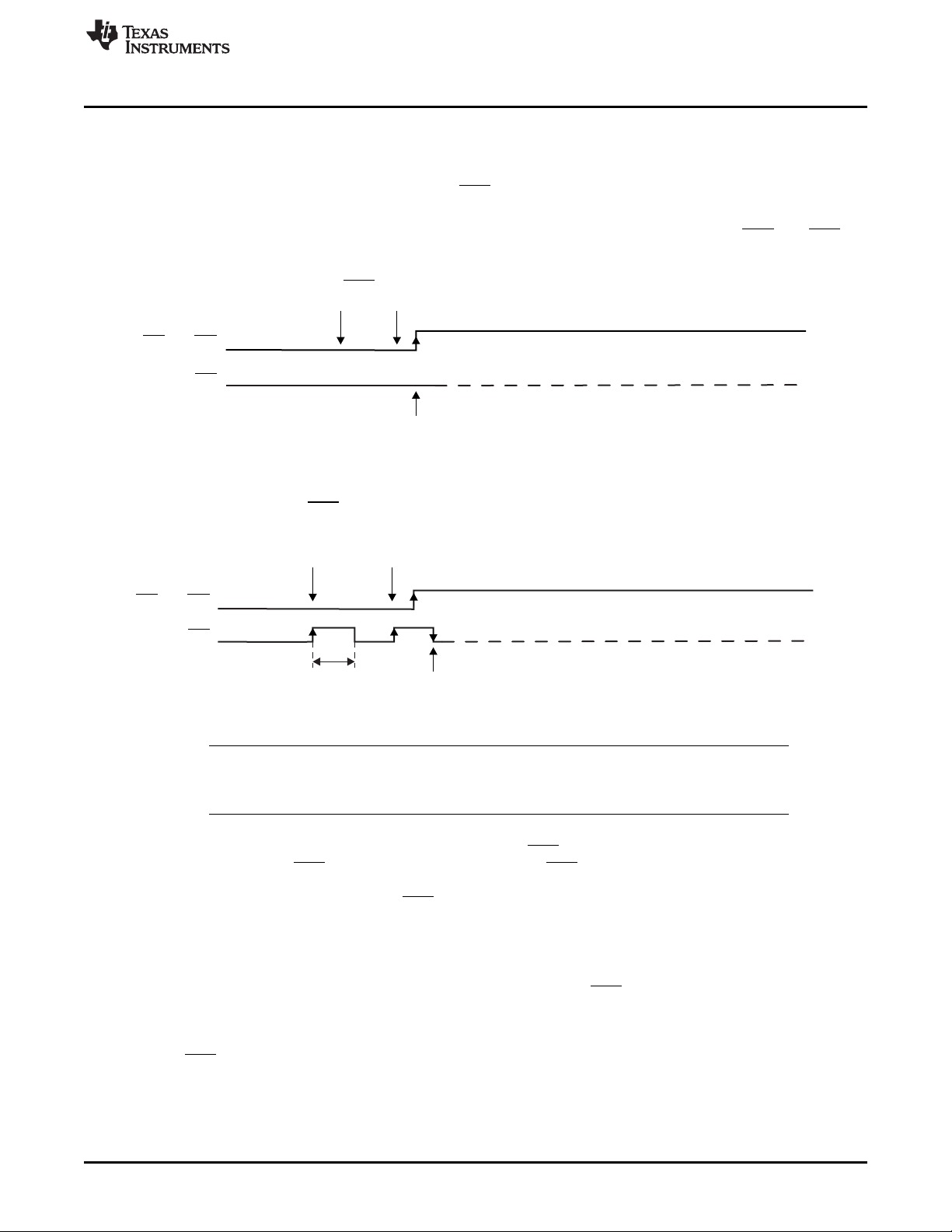
1.3 Standard RESET and BSL Entry Sequence
1.3.1 MSP430 Devices With Shared JTAG Pins
Applying an appropriate entry sequence on the RST/NMI and TEST pins forces the MSP430 MCU to start
program execution at the BSL RESET vector instead of at the RESET vector located at address FFFEh.
If the application interfaces with a computer UART, these two pins may be driven by the DTR and RTS
signals of the serial communication port (RS232) after passing level shifters. Detailed descriptions of the
hardware and related considerations can be found in Section 4. The normal user reset vector at FFFEh is
used if TEST is kept low while RST/NMI rises from low to high (standard method, see Figure 1).
Figure 1. Standard RESET Sequence
The BSL program execution starts when the TEST pin has received a minimum of two positive transitions
and if TEST is high while RST/NMI rises from low to high (BSL entry method, see Figure 2). This level
transition triggering improves BSL start-up reliability. The first high level of the TEST pin must be at least
t
(see device-specific data sheet for t
SBW, En
SBW, En
Introduction
parameter).
Figure 2. BSL Entry Sequence at Shared JTAG Pins
NOTE: The recommended minimum time for pin states is 250 ns. See the device-specific errata for
any differences, because some 5xx and 6xx device revisions require specific entry
sequences.
The TEST signal is normally used to switch the port pins between their application function and the JTAG
function. In devices with BSL functionality, the TEST and RST/NMI pins are also used to invoke the BSL.
To invoke the BSL, the RST/NMI pin must be configured as RST and must be kept low while pulling the
TEST pin high and while applying the next two edges (falling, rising) on the TEST pin. The BSL is started
after the TEST pin is held low after the RST/NMI pin is released (see Figure 2).
1.3.1.1 Factors That Prevent BSL Invocation With Shared JTAG Pins
The BSL is not started by the BSL RESET vector if:
• There are fewer than two positive edges at the TEST pin while RST/NMI is low.
• JTAG has control over the MSP430 MCU resources.
• The supply voltage, VCC, drops below its threshold, and a power-on reset (POR) is executed.
• The RST/NMI pin is configured for NMI functionality (the NMI bit is set).
SLAU319S–July 2010–Revised April 2018
Submit Documentation Feedback
MSP430™ Flash Device Bootloader (BSL)
Copyright © 2010–2018, Texas Instruments Incorporated
5
RST DTR/NMI ( )
TCK ( )RTS
Bootloader Starts
Introduction
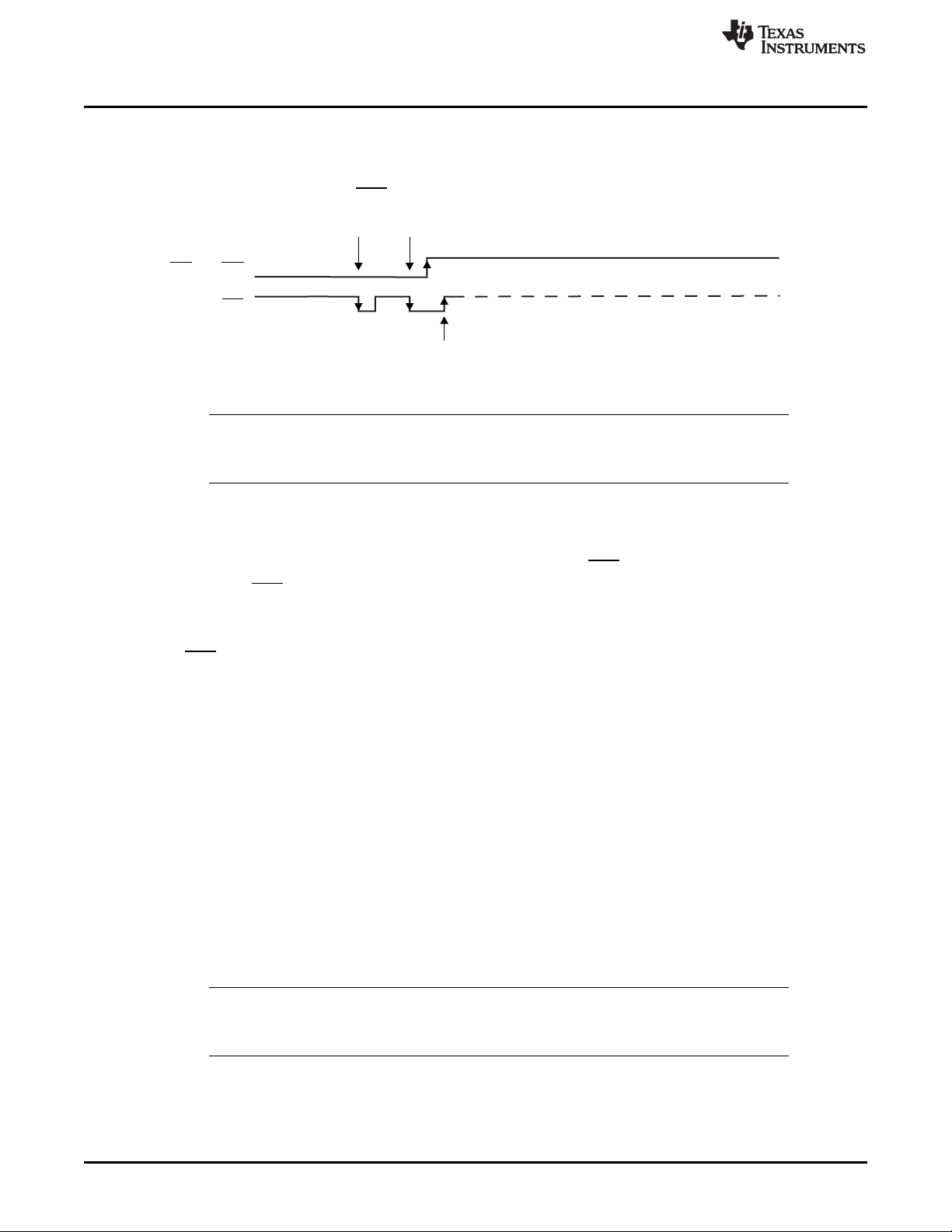
1.3.2 MSP430 Flash Devices With Dedicated JTAG Pins
Devices with dedicated JTAG pins use the TCK pin instead of the TEST pin.
The BSL program execution starts whenever the TCK pin has received a minimum of two negative
transitions and TCK is low while RST/NMI rises from low to high (BSL entry method, see Figure 3). This
level transition triggering improves BSL start-up reliability.
Figure 3. BSL Entry Sequence at Dedicated JTAG Pins
NOTE: The recommended minimum time for pin states is 250 ns. See the device-specific errata for
any differences, because some 5xx and 6xx device revisions have specific entry sequence
requirements.
1.3.2.1 Factors That Prevent BSL Invocation With Dedicated JTAG Pins
The BSL is not started by the BSL RESET vector if:
• There are fewer than two negative edges at the TCK pin while RST/NMI is low.
• TCK is high if RST/NMI rises from low to high.
• JTAG has control over the MSP430 MCU resources.
• The supply voltage, VCC, drops below its threshold, and a power-on reset (POR) is executed.
• The RST/NMI pin is configured for NMI functionality (the NMI bit is set).
www.ti.com
1.3.3 Devices With USB
Devices with USB are invoked when either of the following two conditions are met while the device is
powered by VBUS:
• The device is powered up by USB and the reset vector is blank.
• The device powers up with the PUR pin tied to V
1.4 UART Protocol
The UART protocol applied here is defined as:
• Baud rate is fixed to 9600 baud in half-duplex mode (one sender at a time).
• Start bit, 8 data bits (LSB first), an even parity bit, 1 stop bit.
• Handshake is performed by an acknowledge character.
• Minimum time delay before sending new characters after characters have been received from the
MSP430 BSL: 1.2 ms
NOTE: Applying baud rates other than 9600 baud at initialization results in communication problems
or violates the flash memory write timing specification. The flash memory may be extensively
stressed or may react with unreliable program or erase operations.
USB
.
6
MSP430™ Flash Device Bootloader (BSL)
Copyright © 2010–2018, Texas Instruments Incorporated
SLAU319S–July 2010–Revised April 2018
Submit Documentation Feedback

www.ti.com
1.5 USB Protocol
The USB protocol applied here is defined as:
• HID protocol with one input endpoint and one output endpoint. Each endpoint has a length of 64 bytes.
• VID: 0x2047
• PID: 0x0200
Introduction
SLAU319S–July 2010–Revised April 2018
Submit Documentation Feedback
MSP430™ Flash Device Bootloader (BSL)
Copyright © 2010–2018, Texas Instruments Incorporated
7
Bootloader Protocol – 1xx, 2xx, and 4xx Families
2 Bootloader Protocol – 1xx, 2xx, and 4xx Families
2.1 Synchronization Sequence
Before sending any command to the BSL, a synchronization character (SYNC) with its value of 80h must
be sent to the BSL. This character is necessary to calculate all the essential internal parameters, which
maintain UART and flash memory program and erase timings. It provides the BSL system time reference.
When this is received, an acknowledge DATA_ACK = 90h is sent back by the BSL to confirm successful
reception.
This sequence must be done before every command that is sent to the BSL.
NOTE: The synchronization character is not part of the Data Frame described in Section 2.4.
2.2 Commands
Two categories of commands are available: commands that require a password and commands that do
not require a password. The password protection safeguards every command that potentially allows direct
or indirect data access.
2.2.1 Unprotected Commands
• Receive password
• Mass erase (erase entire flash memory, main as well as information memory)
• Transmit BSL version (V1.50 or higher or in loadable BL_150S_14x.txt but not V2.x BSLs)
• Change baud rate (V1.60 or V1.61 or V2.0x or in loadable BL_150S_14x.txt)
www.ti.com
2.2.2 Password Protected Commands
• Receive data block to program flash memory, RAM, or peripherals
• Transmit data block
• Erase segment
• Erase check (present in V1.60 or higher or in loadable BL_150S_14x.txt)
• Set Memory Offset (present in V2.12 or higher)
• Load program counter and start user program
• Change baud rate (BSL versions lower than V1.60 and higher than V2.10)
2.3 Programming Flow
The write access (RX data block command) to the flash memory, RAM, or peripheral modules area is
executed online. That means a data byte or word is processed immediately after receipt, and the write
cycle is finished before a following byte or word has completely arrived. Therefore, the entire write time is
determined by the baud rate, and no buffering mechanism is necessary.
Data sections located below the flash memory area address are assumed to be loaded into the RAM or
peripheral module area and, thus, no specific flash control bits are affected.
NOTE: If control over the UART protocol is lost, either by line faults or by violating the data frame
conventions, the only way to recover is to rerun the BSL entry sequence to initiate another
BSL session.
8
MSP430™ Flash Device Bootloader (BSL)
Copyright © 2010–2018, Texas Instruments Incorporated
SLAU319S–July 2010–Revised April 2018
Submit Documentation Feedback
www.ti.com
2.4 Data Frame
To ensure high data security during the data transmission, a data frame protocol called serial standard
protocol (SSP) is used. The BSL is considered the receiver in Table 2.
2.4.1 Data-Stream Structure
• The first eight bytes (HDR through LH) are mandatory (xx represents dummy data).
• Data bytes D1 to Dn are optional.
• Two bytes (CKL and CKH) for checksum are mandatory.
• Acknowledge done by the BSL is mandatory, except with the TX data block and TX BSL version
commands.
Bootloader Protocol – 1xx, 2xx, and 4xx Families
Table 2. Data Frame of BSL Commands
Received
BSL
Command
RX data block 80 12 n n AL AH n–4 0 D1 D2 … Dn–4 CKL CKH ACK
RX password 80 10 24 24 xx xx xx xx D1 D2 … D20 CKL CKH ACK
Erase segment 80 16 04 04 AL AH 02 A5 – – – – CKL CKH ACK
Erase main or info 80 16 04 04 AL AH 04 A5 – – – – CKL CKH ACK
Mass erase 80 18 04 04 xx xx 06 A5 – – – – CKL CKH ACK
Erase check 80 1C 04 04 AL AH LL LH – – – – CKL CKH ACK
Change baud rate 80 20 04 04 D1 D2 D3 xx – – – – CKL CKH ACK
Set mem offset 80 21 04 04 xx xx AL AH – – – – CKL CKH ACK
Load PC 80 1A 04 04 AL AH xx xx – – – – CKL CKH ACK
TX data block 80 14 04 04 AL AH n 0 – – – – CKL CKH –
BSL responds 80 xx n n D1 D2 ... ... … ... … Dn CKL CKH –
TX BSL version 80 1E 04 04 xx xx xx xx – – – – CKL CKH –
BSL responds 80 xx 10 10 D1 D2 ... ... … … … D10 CKL CKH –
(1)
All numbers are bytes in hexadecimal notation.
(2)
ACK is sent back by the BSL.
(3)
The synchronization sequence is not part of the data frame.
(4)
The erase check and TX BSL version commands are members of the standard command set in BSLs V1.50 or higher but
excluding 2.x BSLs.
(5)
The change baud rate command is not a member of the standard command set (it is available in V1.60 or higher or in loadable
BL_150S_14x.txt).
(6)
Abbreviations:
HDR: Header. Any value between 80h and 8Fh (normally 80h).
CMD: Command identification
L1, L2: Number of bytes consisting of AL through Dn. Restrictions: L1 = L2, L1 < 255, L1 even
AL, AH: Block start address or erase (check) address or jump address LO or HI byte
LL, LH: Number of pure data bytes (250 max) or erase information LO or HI byte or block length of erase check (FFFFh max)
D1 … Dn: Data bytes
CKL, CKH: 16-bit checksum LO or HI byte
xx: Can be any data
–: No character (data byte) received or transmitted
ACK: The acknowledge character returned by the BSL. Can be either DATA_ACK = 90h: Frame was received correctly,
command was executed successfully, or DATA_NAK = A0h: Frame not valid (for example, wrong checksum, L1 ≠ L2), command
is not defined, is not allowed, or was executed unsuccessfully.
n: Number of bytes consisting of AL through Dn
HDR CMD L1 L2 AL AH LL LH D1 D2…Dn CKL CKH ACK
(1)(2)(3) (4)(5)(6)
SLAU319S–July 2010–Revised April 2018
Submit Documentation Feedback
MSP430™ Flash Device Bootloader (BSL)
Copyright © 2010–2018, Texas Instruments Incorporated
9

Bootloader Protocol – 1xx, 2xx, and 4xx Families
2.4.2 Checksum
The 16-bit (2-byte) checksum is calculated over all received or transmitted bytes B1 to Bn in the data
frame, except the checksum bytes themselves, by XORing words (two successive bytes) and inverting the
result.
This means that B1 is always the HDR byte and Bn is the last data byte just before the CKL byte.
Formula
CHECKSUM = INV [ (B1 + 256 × B2) XOR (B3 + 256 × B4) XOR … XOR (Bn–1 + 256 × Bn) ]
or
CKL = INV [ B1 XOR B3 XOR … XOR Bn–1 ]
CKH = INV [ B2 XOR B4 XOR … XOR Bn ]
2.4.3 Example Sequence
The following example shows a request to read the memory of the MSP430 MCU from location 0x0F00.
All values shown below are represented in hexadecimal format.
TO BSL: 80
(Synchronization character sent to the BSL)
FROM BSL: 90
(Acknowledge from BSL)
TO BSL: 80 14 04 04 00 0F 0E 00 75 E0
(Send Command to read memory from 0x0F00, length 0x000E)
FROM BSL: 80 00 0E 0E F2 13 40 40 00 00 00 00 00 00 02 01 01 01 C0 A2
(Returned values from BSL)
www.ti.com
2.4.4 Commands – Detailed Description
See Table 2.
2.4.4.1 General
Following the header byte HDR (80h) and the command identification CMD, the frame length bytes L1 and
L2 (which must be equal) hold the number of bytes following L2, excluding the checksum bytes CKL and
CKH.
Bytes AL, AH, LL, LH, D1...Dn are command-specific. However, the checksum bytes CKL (low byte) and
CKH (high byte) are mandatory.
If the data frame has been received correctly and the command execution was successful, an
acknowledge character DATA_ACK = 90h is sent back by the BSL. Incorrectly received data frames,
unsuccessful operations, and commands that are locked or not defined are confirmed with a DATA_NAK =
A0h.
NOTE: BSL versions lower than V1.30 support only byte-access operations. Therefore, the
peripheral module addresses at 0100h to 01FFh cannot be accessed correctly, because they
are word-oriented. In version V1.30 and higher, addresses 0000h to 00FFh are accessed in
byte mode; all others are accessed in word mode.
2.4.4.2 RX Data Block
The receive data block command is used for any write access to the flash memory, RAM, or peripheral
module control registers at 0000h to 01FFh. It is password protected.
The 16-bit even-numbered block start address is defined in AL (low byte) and AH (high byte). The 16-bit
even-numbered block length is defined in LL (low byte) and LH (high byte). Because pure data bytes are
limited to a maximum of 250, LH is always 0.
10
MSP430™ Flash Device Bootloader (BSL)
Copyright © 2010–2018, Texas Instruments Incorporated
SLAU319S–July 2010–Revised April 2018
Submit Documentation Feedback
www.ti.com
The following data bytes are succeeded by the checksum bytes CKL (low byte) and CKH (high byte). If
the receipt and programming of the appropriate data block was successful, an acknowledge character
DATA_ACK is sent back by the BSL. Otherwise, the BSL confirms with a DATA_NAK.
NOTE: BSL versions V1.40 and higher support online verification inside the MSP430 MCU for
addresses 0200h to FFFFh, which reduces programming and verification time by 50%.
Online verification means that the data is immediately verified with the data that is written
into the flash without transmitting it again. In case of an error, the loadable bootloader
BL_150S_14x.txt additionally stores the first incorrectly written location address+3 into the
error address buffer in the RAM at address 0200h (021Eh for F14x devices).
2.4.4.3 RX Password
The receive password command is used to unlock the password-protected commands, which perform
reading, writing, or segment-erasing memory access. It is not password protected.
Neither start address nor block length information is necessary, because the 32-byte password is always
located at addresses FFE0h to FFFFh. Data bytes D1 to D20h hold the password information starting with
D1 at address FFE0h.
The BSL responds with DATA_ACK when the package from the host is received correctly and has valid
content as shown in Table 2. The DATA_ACK does not reflect that the password is correct (that is, it
matches the content of FFE0h to FFFFh) or incorrect. If an incorrect password is sent, other commands
will respond with DATA_NAK, because the BSL is still locked.
After the protected commands are unlocked, they remain unlocked until another BSL entry is initiated.
Bootloader Protocol – 1xx, 2xx, and 4xx Families
2.4.4.4 Mass Erase
The mass erase command erases the entire flash memory area (main memory plus information memory,
see corresponding data sheet). This command is not password protected.
All parameters shown in Table 2 are mandatory. After erasing, an acknowledge character DATA_ACK is
sent back by the BSL.
Mass erase initializes the password area to 32 times 0FFh.
NOTE: BSL versions 2.01 and higher support automatic clearing of the LOCKA bit, which protects
information memory.
When entering the BSL by cold start (that is, by applying the BSL hardware entry sequence
on the RST and TST pins), the LOCKA bit is automatically unlocked. A mass erase that is
executed during BSL communication erases all parts of information memory and also main
memory.
When entering the BSL by warm start (that is, by jumping to the BSL application from a
software function), the LOCKA bit is not automatically unlocked. A mass erase performed in
this state does not erase the information memory. Therefore, when the BSL is called by
software, the user application must ensure that LOCKA is cleared before initialization of the
BSL, so a mass erase command can erase the information memory.
2.4.4.5 Erase Segment
The erase segment command erases specific flash memory segments. It is password protected.
The address bytes AL (low byte) and AH (high byte) select the appropriate segment. Any even-numbered
address within the segment to be erased is valid. After segment erasing, an acknowledge character
DATA_ACK is sent back by the BSL (V1.40 or lower).
SLAU319S–July 2010–Revised April 2018
Submit Documentation Feedback
MSP430™ Flash Device Bootloader (BSL)
Copyright © 2010–2018, Texas Instruments Incorporated
11

Bootloader Protocol – 1xx, 2xx, and 4xx Families
BSL versions V1.60 or higher perform a subsequent erase check of the corresponding segment and
respond with a DATA_NAK if the erasure was not successful. In this case, the first non-erased location
address + 1 is stored in the error address buffer in the RAM at address 0200h (021Eh for F14x devices).
In this version, a problem occurs if only one of the information memory segments is erased. In this case,
an error is reported, because an automatic erase check over the whole information memory is performed.
As a solution, either erase the whole information memory or do a separate erase check after the erase,
even if the erase reported an error.
Erase segment 0 clears the password area and, therefore, the remaining password is 32 times 0FFh.
When applying LL = 0x04 and LH = 0xA5, a mass erasure of only the main memory is performed. Indeed,
this command must be executed a minimum of 12 times to achieve a total erasure time of >200 ms. No
subsequent erase check of the entire main memory is done. Use the erase check command additionally.
Check the device data sheet for more information on the cumulative (mass) erase time that must be met
and the number of erase cycles required.
2.4.4.6 Erase Main or Info
The erase main or info command erases specific flash memory section. It is password protected.
The address bytes AL (low byte) and AH (high byte) select the appropriate section of flash (main or
information). Any even-numbered address within the section to be erased is valid.
2.4.4.7 Erase Check
The erase check command verifies the erasure of flash memory within a certain address range. It is
password protected.
The 16-bit block start address is defined in AL (low byte) and AH (high byte). The 16-bit block length is
defined in LL (low byte) and LH (high byte). Both can be either even or odd numbered to allow odd
boundary checking.
If the erase check of the appropriate data block was successful (all bytes contain 0FFh), an acknowledge
character DATA_ACK is sent back by the BSL. Otherwise, the BSL confirms with a DATA_NAK and the
first non-erased location address + 1 is stored in the error address buffer at address 0200h (021Eh for
F14x devices).
www.ti.com
NOTE: This command is not a member of the standard command set. It is implemented in BSL
version V1.60 and higher or in the loadable bootloader BL_150S_14x.txt.
2.4.4.8 Change Baud Rate
The change baud rate command offers the capability of transmissions at higher baud rates than the
default 9600 baud. With faster data transition, shorter programming cycles can be achieved, which is
especially important with large flash memory devices. This command is not password protected.
Three control bytes (D1 to D3) determine the selected baud rate. D1 and D2 set the processor frequency
(f ≥ f
), D3 indirectly sets the flash timing generator frequency (f
min
D1: F1xx: Basic clock module control register DCOCTL (DCO.2 to DCO.0)
F2xx: Basic clock module control register DCOCTL (DCO.2 to DCO.0)
F4xx: FLL+ system clock control register SCFI0 (D, FN_8 to FN_2)
D2: F1xx: basic clock module control register BCSCTL1 (XT2Off, Rsel.2 to Rsel.0)
F2xx: basic clock module control register BCSCTL1 (XT2Off, Rsel.2 to Rsel.0)
F4xx: FLL+ system clock control register SCFI1 (N
D3 0: 9600 baud
1: 19200 baud
2: 38400 baud
12
MSP430™ Flash Device Bootloader (BSL)
FTGmin
)
DCO
Copyright © 2010–2018, Texas Instruments Incorporated
≤ f
≤ f
FTG
SLAU319S–July 2010–Revised April 2018
). In detail:
FTGmax
Submit Documentation Feedback
www.ti.com
After receiving the data frame, an acknowledge character DATA_ACK is sent back, and the BSL becomes
prepared for the selected baud rate. TI recommends that the BSL communication program wait
approximately 10 ms between baud rate alteration and the next data transmission to give the BSL clock
system time to stabilize.
Bootloader Protocol – 1xx, 2xx, and 4xx Families
NOTE: The highest achievable baud rate depends on various system and environment parameters
like supply voltage, temperature range, and minimum and maximum processor frequency.
See the device-specific data sheet.
NOTE: This command is implemented on BSL versions V1.60 or higher or available in the loadable
bootloader BL_150S_14x.txt.
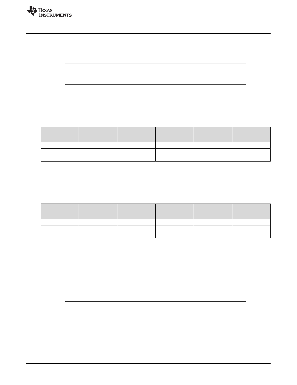
(1)
Program and
Verify 60 KB
(4)
(sec)
Baud Rate
(baud)
Table 3. Recommendations for MSP430F149 [MSP430F449]
Processor
Frequency, f
(2)
(MHz)
(TA= 25°C, VCC= 3.0 V, f
D1 DCOCTL
min
[SCFI0]
(3)
D2 BCSCTL1
[SCFI1]
= 6.7 MHz)
max
(3)
D3
(3)
9600 (init) 1.05 0x80 [00] 0x85 [98] 00 [00] 78 + 3.7 [0.0]
19200 2.1 0xE0 [00] 0x86 [B0] 01 [01] 39 + 3.7 [2.4]
38400 4.2 0xE0 [00] 0x87 [C8] 02 [02] 20 + 3.7 [2.4]
(1)
Values in brackets [ ] apply to MSP430F449.
(2)
The minimum processor frequency is lower than in the standard ROM BSL (see Section 2.9.3, Initialization Status).
(3)
D1 to D3 are bytes in hexadecimal notation.
(4)
Additional 3.7 [2.4] seconds result from loading, verifying, and launching the loadable BSL.
Baud Rate
(baud)
Processor
Frequency, f
(2)
(MHz)
Table 4. Recommendations for MSP430F2131
(TA= 25°C, VCC= 3.0 V, f
D1 DCOCTL
min
[SCFI0]
(3)
D2 BCSCTL1
[SCFI1]
= 6.7 MHz)
max
(3)
D3
(1)
(3)
Program and
Verify 60 KB
(sec)
9600 (init) 1.05 0x80 0x85 00 78
19200 2.1 0x00 0x8B 01 39
38400 4.2 0x80 0x8C 02 20
(1)
Values in brackets [ ] are related to MSP430F449.
(2)
The minimum processor frequency is lower than in the standard ROM BSL (see Section 2.9.3, Initialization Status).
(3)
D1 to D3 are bytes in hexadecimal notation.
2.4.4.9 Set Memory Offset
An offset for the memory pointer can be set for devices that have more than 64KB of memory, specifically
MSP430X architecture devices. The value for the memory offset is used as the memory pointer’s upper
word.
Memory Address = Offset Value << 16 + Actual Address
NOTE: This command is implemented on BSL versions V2.12 and higher.
2.4.4.10 Load PC
The load program counter command directs the program counter (register R0) to any location within the
entire address range. It is password protected.
After receiving the data frame, an acknowledge character (DATA_ACK) is sent back by the BSL. Then the
selected address is moved into the program counter. The program flow continues operation there, and the
BSL session is terminated.
SLAU319S–July 2010–Revised April 2018
Submit Documentation Feedback
MSP430™ Flash Device Bootloader (BSL)
Copyright © 2010–2018, Texas Instruments Incorporated
13

Bootloader Protocol – 1xx, 2xx, and 4xx Families
Be aware that password protection is not active at this time. Jumping to the user application does not
reset the device and, therefore, the register configuration from the BSL application is kept. This might
cause unexpected behavior in the user application. One example is the blink LED application, which does
not have any clock module configuration (so it uses the default 1-MHz clock) and will blink faster, because
the clock module is set by the BSL application to run at 8 MHz.
2.4.4.11 TX Data Block
The transmit data block command is used for any read access to the flash memory, RAM, or peripheral
module control registers at 0000h to 01FFh. It is password protected.
The 16-bit block start address is defined in AL (low byte) and AH (high byte). The 16-bit block length is
defined in LL (low byte) and LH (high byte). Because pure data bytes are limited to a maximum of 250, LH
is always 0. The checksum bytes CKL (low byte) and CKH (high byte) immediately follow this information.
Now the BSL responds with the requested data block. After transmitting HDR, dummy CMD, L1 and L2,
The BSL sends data bytes D1 through Dn, followed by the checksum bytes CKL (low byte) and CKH (high
byte). No acknowledge character is necessary.
2.4.4.12 TX BSL Version
The transmit BSL version command gives the user information about chip identification and bootloader
software version. It is not password protected.
The values for AL, AH, LL, and LH can be any data, but must be transmitted to meet the protocol
requirements. The checksum bytes CKL (low byte) and CKH (high byte) follow this information.
After that, the BSL responds with a 16-byte data block. After transmitting HDR, dummy CMD, L1 and L2,
the BSL sends data bytes D1 through D16 (decimal), followed by the checksum bytes CKL (low byte) and
CKH (high byte). No acknowledge character is necessary.
D1, D2 and D11, D12 (decimal) hold the specific information:
• D1: Device family type (high byte)
• D2: Device family type (low byte)
• D11: BSL version (high byte)
• D12: BSL version (low byte)
The remaining 12 bytes are for internal use only.
www.ti.com
2.5 Loadable BSL
For upgrading the BSL functionality, sometimes it is suitable to load a higher version of BSL into the RAM
of a device and apply the latest innovations. To do so, use the following BSL commands:
• RX password (unlock password protection for following commands)
• RX data block (code of loadable BSL, code section address ≥ 220h)
• TX data block (for verification)
• RX data block (get start address from first code section address)
• Load program counter PC (with start address of loadable BSL)
• Wait at least 5 ms until the new loaded BSL has executed the initialized routine
• RX password (unlock password protection for loaded BSL)
• Perform any command (with loaded BSL)
The following loadable BSLs are available:
• BL_150S_14x.txt is a complete BSL for the F14x and F13x family with BSL version 1.10. All features
of BSL version V1.60 are supported. Because its code size is larger than 1KB, it can be used only in
F1x8 and F1x9 devices. The error address buffer address for RX Block, Erase Segment, and Erase
Check commands is 021Eh. BL_150S_14x.txt could also be used as a replacement for PATCH.txt.
• BS_150S_14x.txt is a small BSL with reduced command set for the F14x and F13x family with BSL
version 1.10. Because its code size is smaller than 512B, it can be used in F1x4 up to F1x9 devices.
14
MSP430™ Flash Device Bootloader (BSL)
Copyright © 2010–2018, Texas Instruments Incorporated
SLAU319S–July 2010–Revised April 2018
Submit Documentation Feedback

www.ti.com
The following commands of BSL version V1.60 are supported: Change Baud Rate, RX Block (with
online verification), Erase Check, and Load PC. If a TX Block command (redirected to ROM BSL) is
needed (for example, for transmitting error address or standalone Verify), the RAM BSL must be
invoked again by the Load PC command. The error address buffer address for RX Block and Erase
Check commands is 021Eh. BS_150S_14x.txt could also be used as a partial replacement for
PATCH.txt. No password is required, as the RX password command is removed.
For more information on downloading a different bootloader, see Application of Bootstrap Loader in
MSP430 With Flash Hardware and Software Proposal.
Third-party software normally uses loadable BSLs to perform most functions, like online verification, and to
improve speed for appropriate devices.
2.6 Exiting the BSL
To exit the BSL mode, two possibilities are provided:
• The microcontroller continues operation at a defined program address invoked by the load program
counter command. Be aware that the password protection is not active at this time. In this case, the
user application should ensure that the flash is locked, as this is not done by the BSL. Leaving the BSL
unlocked increases the risk of erroneously modifying the flash due to system or software errors. On
2xx devices, the correct setting of the LOCKA bit should also be checked.
• Applying the standard RESET sequence (see Figure 1) forces the microcontroller to start with the user
reset vector at address 0FFFEh.
2.7 Password Protection
The password protection prohibits every command that potentially allows direct or indirect data access.
Only the unprotected commands like mass erase and RX password (optionally, TX BSL version and
change baud rate) can be performed without prior receipt of the correct password after BSL entry.
Applying the RX password command for receiving the correct password unlocks the remaining
commands.
After it is unlocked, it remains unlocked until initiating another BSL entry.
The password itself consists of the 16 interrupt vectors located at addresses FFE0h to FFFFh (256 bits),
starting with the first byte at address FFE0h. After mass erase and with unprogrammed devices, all
password bits are logical high (1).
BSL versions 2.00 and higher have enhanced security features. These features are controlled by the flash
data word located beneath the interrupt vector table addresses (for example, for the MSP430F2131,
address 0xFFDE). If this word contains:
• 0x0000: The flash memory is not erased if an incorrect BSL password has been received by the target.
• 0xAA55: The BSL is disabled. This means that the BSL is not started with the default initialization
sequence shown in Section 1.3.
• All other values: If an incorrect password is transmitted, the entire flash memory address space is
erased automatically.
Bootloader Protocol – 1xx, 2xx, and 4xx Families
NOTE: The user must take care of password update after modifying the interrupt vectors and
initiating another BSL session. TI strongly recommends initializing unused interrupt vectors to
increase data security.
2.8 Code Protection Fuse
After the JTAG fuse (code protection fuse) is blown, no further access to the JTAG test feature is possible.
The only way to get any memory read or write access is through the bootloader by applying the correct
password.
However, it is not possible for the BSL to blow the JTAG fuse. If fuse blowing is needed, use JTAG
programming techniques.
SLAU319S–July 2010–Revised April 2018
Submit Documentation Feedback
MSP430™ Flash Device Bootloader (BSL)
Copyright © 2010–2018, Texas Instruments Incorporated
15
Bootloader Protocol – 1xx, 2xx, and 4xx Families
2.9 BSL Internal Settings and Resources
The following paragraphs describe BSL internal settings and resources. Because the same device may
have implemented different BSL versions, it is very important for the BSL communication program to know
the settings and resources. Resources could be either device dependent (for example, RX or TX pins) or
BSL-version dependent (for example, byte or word access). The following sections describe the possible
variations.
2.9.1 Chip Identification and BSL Version
The upper 16 bytes of the boot-ROM (0FF0h to 0FFFh) hold information about the device and BSL
version number in BCD representation. This is common for all devices and BSL versions:
• 0FF0h to 0FF1h: Chip identification (for example, F413h for an F41x device).
• 0FFAh to 0FFBh: BSL version number (for example, 0130h for BSL version V1.30).
See the MSP430 device to BSL version assignment in Section 5.
2.9.2 Vectors to Call the BSL Externally
The entry part of the boot ROM holds the calling vectors for BSL access by program:
• 0C00h: Vector for cold start (mnemonic: BR &0C00h) (recommended)
• 0C02h: Vector for warm start (mnemonic: BR &0C02h). V1.30 or higher.
• 0C04h: Vectors for future use. This table is expandable.
www.ti.com
NOTE: A warm start does not modify the stack pointer. Additionally, the status register for the BSL is
not cleared, which could cause a warm started BSL to come up in an unlocked state. Warm
start possibility exists only for highly specialized instances where it is absolutely mandatory
that a running application be returned to after a BSL session without resetting the device. In
almost all cases, it is better to start the BSL from user code by calling the cold start vector.
16
MSP430™ Flash Device Bootloader (BSL)
Copyright © 2010–2018, Texas Instruments Incorporated
SLAU319S–July 2010–Revised April 2018
Submit Documentation Feedback

www.ti.com
2.9.3 Initialization Status
When activating the BSL, the following settings take effect:
• Stop watchdog timer
• Disable all interrupts (GIE = 0)
• V1.10
The stack pointer is not modified, except when it points to an excluded memory area. If so, it is
initialized to 021Ah.
V1.30 or higher
The stack pointer is not modified if the BSL is called by the program through the warm-start vector. It is
initialized to 0220h if the BSL starts by the BSL RESET sequence or is called by the program through
the cold-start vector.
• F1xx
Determine basic clock module so that minimum frequency is 1.5 MHz:
BCSCTL1 = 85h (RSEL = 5, XT2Off = 1)
DCOCTL = 80h (DCO = 4, MOD = 0)
BCSCTL2 = 00h only at cold start
SR: SCG1 = 00h (SMCLK on) only at cold start
F2xx
Determine basic clock module so that minimum frequency is 1.5 MHz:
BCSCTL1 = 88h (RSEL = 8, XT2Off = 1)
DCOCTL = 80h (DCO = 4, MOD = 0)
BCSCTL2 = 00h only at cold start
SR: SCG1 = 00h (SMCLK on) only at cold start
F4xx
Determine FLL oscillator and system clock so that minimum frequency is 1.5 MHz:
SCFI0 = 00h (D = 0, FN_x = 0)
SCFI1 = 98h (N_DCO)
SCFQCTL: (M = 0)
SR: SCG0 = 1 (FLL loop control off)
FLL_CTL1 = 00h only at cold start
• SW-UART: Timer_A operates in continuous mode with MCLK source (Div = 1)
CCR0 used for compare
CCTL0 used for polling of CCIFG0
• TX pin is set to output high for RS232 idle state
• RX pin is set to input
• Password-protected commands are locked (only at cold start)
After system initialization, the BSL is ready for operation and waits for the first synchronization sequence
(SS) followed by a data frame containing the first BSL command.
Bootloader Protocol – 1xx, 2xx, and 4xx Families
SLAU319S–July 2010–Revised April 2018
Submit Documentation Feedback
MSP430™ Flash Device Bootloader (BSL)
Copyright © 2010–2018, Texas Instruments Incorporated
17

Bootloader Protocol – 1xx, 2xx, and 4xx Families
2.9.4 Memory Allocation and Resources
• The BSL program code is located in the boot-ROM area 0C00h to 0FEFh.
• Addresses 0FF0h to 0FFFh hold the device identification.
• The BSL variables occupy the RAM area
– 0200h to 0213h (V1.10)
– 0200h to 0219h (V1.30 or higher)
• The BSL stack occupies the RAM area
– 0214h to 0219h (V1.10)
– 021Ah to 021Fh (V1.30 or higher, only at cold start)
• The working registers used are:
– R5 to R9 (V1.30 or lower) or
– R5 to R10 (V1.40) or
– R5 to R11 (V1.60) or
– R5 to R14 (V2.00 or higher)
Their contents are not buffered.
– F1xx and F2xx:
• The basic clock module registers used are:
• DCOCTL at address 056h
• BCSCTL1 at address 057h
– F4xx:
• The FLL oscillator and system clock registers used are:
• SCFI0 at address 050h
• SCFI1 at address 051h
• SCFQCTL at address 052h
• The Timer_A control registers used are:
• TACTL at address 0160h
• CCTL0 at address 0162h
• TAR at address 0170h
• CCR0 at address 0172h
• The flash control registers used are:
• FCTL1 at address 0128h
• FCTL2 at address 012Ah
• FCTL3 at address 012Ch
• No interrupt service is affected.
www.ti.com
18
MSP430™ Flash Device Bootloader (BSL)
Copyright © 2010–2018, Texas Instruments Incorporated
SLAU319S–July 2010–Revised April 2018
Submit Documentation Feedback

www.ti.com
3 Bootloader Protocol – F5xx and F6xx Families
3.1 BSL Data Packet
The BSL data packet has a layered structure. The BSL core command contains the actual command data
to be processed by the BSL. In addition the standard BSL commands, there can be wrapper data before
and after each core command known as the peripheral interface code (PI Code). This wrapper data is
information that is specific to the peripheral and protocol being used, and it contains information that
allows for correct transmission of the BSL core command. Taken together, the wrapper and core
command constitute a BSL data packet.
PI Code BSL Core Command PI Code
3.2 UART Peripheral Interface (PI)
3.2.1 Wrapper
The default BSL430 programmed in each non-USB MSP430F5xx device communicates using a UART
peripheral interface (PI). The UART protocol interface has the format shown in Table 5. All numbers are in
hexadecimal format.
Table 5. UART Protocol Interface
Header Length Length BSL Core Command CKL CKH ACK
0x80 NL NH See Table 9 CKL CKH
Bootloader Protocol – F5xx and F6xx Families
(ACK)
from BSL
3.2.2 Abbreviations
CKL, CKH
CRC checksum high and low bytes. The checksum is computed on bytes in BSL core command
section only. The CRC is computed using the MSP430F5xx CRC module specification (see the CRC
chapter of the MSP430x5xx and MSP430x6xx Family User's Guide for implementation details).
NL, NH
Number of bytes in BSL core data packet, broken into high and low bytes.
ACK
Sent by the BSL after the packet is received to acknowledge receiving the data correctly. This does not
imply the BSL core data is a correct command or that it was executed correctly. ACK signifies only that
the packet was formatted as expected and had a correct checksum.
NOTE: If the PI encounters an error at any stage of receiving the packet, it immediately responds
with the appropriate error message.
3.2.3 Messages
The peripheral interface section of the BSL430 software parses the wrapper section of the BSL data
packet. If there are errors with the data transmission, an error message is sent immediately. An ACK is
sent after all data has been successfully received and does not mean that the command has been
correctly executed (or even that the command was valid) but, rather, that the data packet was formatted
correctly and passed on to the BSL core software for interpretation.
SLAU319S–July 2010–Revised April 2018
Submit Documentation Feedback
MSP430™ Flash Device Bootloader (BSL)
Copyright © 2010–2018, Texas Instruments Incorporated
19

START ADDRESS W ACK DATA PACK DATA ACK
Sent by master
Sent by slave
Bootloader Protocol – F5xx and F6xx Families
Data Meaning
0x00 ACK
0x51 Header incorrect. The packet did not begin with the required 0x80 value.
0x52 Checksum incorrect. The packet did not have the correct checksum value.
0x53 Packet size zero. The size for the BSL core command was given as 0.
0x54 Packet size exceeds buffer. The packet size given is too big for the RX buffer.
0x55 Unknown error
0x56 Unknown baud rate. The supplied data for baud rate change is not a known value.
3.2.4 Interface Specific Commands
The Timer UART protocol interface also accepts the following command when it is transmitted as BSL
core data.
BSL Command CMD AL AM AH Data
Change baud rate 0x52 – – – D1
3.2.4.1 Change Baud Rate
This command changes the baud rate for all subsequently received data packets. The command is
acknowledged with either a single ACK (sent at the current, not the newly selected, baud rate) or an error
byte. No subsequent message packets can be expected.
D1: Valid values
• 0x02: 9600
• 0x03: 19200
• 0x04: 38400
• 0x05: 57600
• 0x06: 115200
www.ti.com
Table 6. UART Error Messages
3.3 I2C Peripheral Interface
3.3.1 I2C Protocol Definition
The I2C protocol used by the BSL is defined as:
• Master must request data from BSL slave.
• 7-bit addressing mode is used, and the slave listens to address 0x48.
• Handshake is performed by an acknowledge character in addition to the hardware ACK.
• Minimum time delay before sending new characters after characters have been received from the
MSP430 BSL is 1.2 ms.
• Repeated starts are not required by the BSL but can be used.
3.3.2 Basic Protocol With Byte Level Acknowledge
20
MSP430™ Flash Device Bootloader (BSL)
Figure 4. Basic Protocol - Byte Level ACK
Copyright © 2010–2018, Texas Instruments Incorporated
SLAU319S–July 2010–Revised April 2018
Submit Documentation Feedback

START ADDRESS W ACK DATA PACK DATA ACK
Sent by master
Sent by slave
www.ti.com
1. Send the START bit
2. Send the slave address
3. Send the Read (R)-1 or Write (W)-0 bit.
4. Wait for or send an acknowledge bit
5. Send or receive the data byte (8 bits)
6. Expect or send acknowledge bit
7. Send the STOP bit
3.3.3 I2C Protocol for BSL - Read From Slave
1. Send a start sequence (S)
2. Send I2C address of Slave with the R/W bit low (even address) (ADDR) + W.
3. Send Data or address of internal address of slave register (NDATA)
4. Send a start sequence again (repeated start) (Res)
5. Send I2C address of slave with the R/W bit high (odd address) (ADDR)
6. Read data byte from slave (RDATA)
7. Send the stop sequence (P)
All BSL wrapper commands from the host (master) are considered as data (represented as NDATA, they
may consist of n number of bytes), and all data read from the slave are also considered data and
represented as RDATA.
The protocol for all communication from Master to Slave is:
From Master → S + ADDR + W + NDATA + ReS + ADDR + R
From Slave → RDATA
From Master → P
Bootloader Protocol – F5xx and F6xx Families
3.3.4 Acknowledge (ACK)
There are two levels of acknowledge.
• The low-level acknowledges indicating reception of each byte that is part of the I2C protocol. This is
managed by the hardware if proper I2C settings are set on the slave registers.
• The high-level acknowledge indicates that the checksum of the BSL core command obtained is correct
and as expected. In some cases, this ACK may indicate the command was properly executed. This is
the first byte of RDATA. If this is NAK (other than 0x00), it indicates that a proper command was not
received and the master should consider that command transmission as a failure. If this is ACK (0x00),
it indicates that the transmission or reception of the command was correct with the right checksum and
that the data which follows is the response, if any, from the slave. The slave may keep the CLK line
low if it needs time to process before it responds to the command.
Figure 5. Byte Level ACK
SLAU319S–July 2010–Revised April 2018
Submit Documentation Feedback
Copyright © 2010–2018, Texas Instruments Incorporated
MSP430™ Flash Device Bootloader (BSL)
21

Bootloader Protocol – F5xx and F6xx Families
3.3.5 Wrapper
The wrapper for the BSL data packet integrates the common UART BSL Core Command packet, but adds
Length, Checksum, and Acknowledge to be used within I2C communication (see Table 7).
Table 7. BSL Core Command Wrapper for I2C
Header Length Length BSL Core Command CKL CKH ACK
0x80 NL NH See Section 3.5 CKL CKH
CKL, CKH
CRC checksum high and low bytes. The checksum is computed on bytes in BSL core command
section only.
NL, NH
Number of bytes in BSL core data packet, broken into high and low bytes.
ACK
Sent by the BSL after the packet is received to acknowledge receiving the data correctly. This does not
imply that the BSL core data is a correct command or that it was executed correctly. ACK signifies only
that the packet was formatted as expected and had a correct checksum.
3.4 USB Peripheral Interface
www.ti.com
(ACK)
from BSL
3.4.1 Wrapper
The Peripheral Interface for the USB bootloader has the wrapper format shown in Table 8. There are no
interface specific commands or replies for the USB BSL. The only variable byte, NL, should describe the
number of bytes contained in the BSL Core Command packet.
Header Length BSL Core Command
0x3F NL See Section 3.5
3.4.2 Hardware Requirements
The USB Peripheral Interface requires the use of a high-frequency oscillator on XT2. For the BSL to
function properly, the oscillator can be 24 MHz, 12 MHz, 8 MHz, or 4 MHz.
3.5 BSL Core Command Structure
The BSL core command is transmitted in the format shown in Table 9. All numbers are in hexadecimal
format.
NOTE: See Section 5.5 for using the following commands with the BSL in the MSP430F5438 (non-A
version).
Table 8. USB Peripheral Interface
Table 9. BSL Core Commands
BSL Command CMD AL AM AH Data
RX Data Block 0x10 (AL) (AM) (AH) D1 ... Dn
RX Data Block Fast 0x1B (AL) (AM) (AH) D1 ... Dn
RX Password 0x11 – – – D1 ... D33
Erase Segment 0x12 (AL) (AM) (AH) –
Unlock and Lock Info 0x13 – – – –
Reserved 0x14 – – – –
22
MSP430™ Flash Device Bootloader (BSL)
SLAU319S–July 2010–Revised April 2018
Submit Documentation Feedback
Copyright © 2010–2018, Texas Instruments Incorporated

www.ti.com
BSL Command CMD AL AM AH Data
Mass Erase 0x15 – – – –
CRC Check 0x16 (AL) (AM) (AH) Length (low byte), Length (high byte)
Load PC 0x17 (AL) (AM) (AH) –
TX Data Block 0x18 (AL) (AM) (AH) Length (low byte), Length (high byte)
TX BSL Version 0x19 – – – –
TX Buffer Size
(1)
The TX Buffer Size command is currently not implemented in the BSL on F5xx and F6xx MCUs.
NOTE: BSLs that are programmed in flash and that communicate by USB contain only a subset of
(1)
the commands shown in Table 9. These commands can be used to load in a full BSL into
RAM for flash programming. The commands in this subset are RX DATA BLOCK FAST, RX
PASSWORD, and LOAD PC.
The supported features can also be determined by the BSL version number as shown in
Section 3.7.3. Examples of how to load a full-featured BSL into RAM are given in the zip file
that is associated with this document (see Section 1.1).
3.5.1 Abbreviations
–
No data required. No delay should be given, and any subsequently required data should be sent as the
immediate next byte.
AL, AM, AH
Address bytes. The low, middle, and upper bytes, respectively, of an address.
D1 ... Dn
Data bytes 1 through n (Note: n must be 4 less than the BSL buffer size.)
Length
A byte containing a value from 1 to 255 describing the number of bytes to be transmitted or used in a
CRC. In the case of multiple length bytes, they are combined together as described to form a larger
value describing the number of required bytes.
Bootloader Protocol – F5xx and F6xx Families
Table 9. BSL Core Commands (continued)
0x1A – – – –
3.5.2 Command Descriptions
RX Data Block
The BSL core writes bytes D1 through Dn starting from the location specified in the address fields.
RX Data Block Fast
This command is identical to RX Data Block, except there is no reply indicating the data was correctly
programmed. It is used primarily to speed up USB programming.
RX Password
The BSL core receives the password contained in the packet and unlocks the BSL protected
commands if the password matches the top 16 words in the BSL interrupt vector table (located
between addresses 0xFFE0 and 0xFFFF). When an incorrect password is given, a mass erase is
initiated. This means all code flash is erased, but not Information Memory.
Erase Segment
The flash segment containing the given address is subjected to an erase.
SLAU319S–July 2010–Revised April 2018
Submit Documentation Feedback
MSP430™ Flash Device Bootloader (BSL)
Copyright © 2010–2018, Texas Instruments Incorporated
23

Bootloader Protocol – F5xx and F6xx Families
Unlock and Lock Info
This command causes the INFO_A lock to toggle to either protect or lock the INFO_A segment. See
the MSP430x5xx and MSP430x6xx Family User's Guide for more detail on this lock. This command
must be sent before an erase segment command for INFO_A but is not required before a mass erase.
Erase Block
The flash block containing the given address is subjected to an erase.
Mass Erase
All code flash in the MSP430 MCU is erased. This function does not erase Information Memory.
CRC Check
The MCU performs a 16-bit CRC check using the CCITT standard. The address given is the first byte
of the CRC check. Two bytes are used for the length.
Load PC
Causes the BSL to begin execution at the given address using a CALLA instruction. As BSL code is
immediately exited with this instruction, no core response can be expected.
TX BSL Version
BSL transmits its version information (see Section 3.7.3 for more details).
TX Buffer Size
The BSL transmits a value that represents the number of bytes available in its data buffer for sending
or receiving BSL core data packets.
www.ti.com
3.6 BSL Security
3.6.1 Protected Commands
To protect data within the device, most core commands are protected. A protected command is
successfully complete only after the device has been unlocked by sending the RX Password command
with the correct password. In addition, commands specific to the peripheral interface are not protected.
Unprotected Commands
RX Password
Mass Erase
Password Protected Commands
RX Data Block to Address (flash or RAM)
TX BSL Version
TX Data Block
Erase Segment
Erase Bank
Set Program Counter
Toggle INFO_A Lock
Erase Main
CRC Check
3.6.2 RAM Erase
At start-up, the BSL performs a RAM erase, writing a constant word to certain RAM locations in a device.
Usually these is the smallest shared RAM addresses within a family. See Section 5 for device specific
information.
24
MSP430™ Flash Device Bootloader (BSL)
Copyright © 2010–2018, Texas Instruments Incorporated
SLAU319S–July 2010–Revised April 2018
Submit Documentation Feedback

www.ti.com
3.7 BSL Core Responses
The BSL core responses are always wrapped in a peripheral interface wrapper with the identical format to
that of received commands. The BSL core can respond in the format shown in Table 10. All numbers are
in hexadecimal format.
3.7.1 Abbreviations
CMD
A required field used to distinguish between a message from the BSL and a data transmission from the
BSL.
MSG
A byte containing a response from the BSL core describing the result of the requested action. This can
either be an error code or an acknowledgment of a successful operation. In cases where the BSL is
required to respond with data (for example, memory, version, CRC, or buffer size), no successful
operation reply occurs, and the BSL core immediately sends the data.
D1, Dx
Data bytes containing the requested data.
DL, DH
Data low and high bytes, respectively, of a requested 16-bit CRC value.
NL, NH
Data bytes describing the length of the buffer size in bytes. To manage sizes above 255, the size is
broken up into a low byte and a high byte.
Bootloader Protocol – F5xx and F6xx Families
Table 10. BSL Core Responses
BSL Response CMD Data
Data Block 0x3A D1 ... Dn
BSL Version 0x3A D1 ... D4
CRC Value 0x3A DL, DH
Buffer Size 0x3A NL, NH
Message 0x3B MSG
SLAU319S–July 2010–Revised April 2018
Submit Documentation Feedback
MSP430™ Flash Device Bootloader (BSL)
Copyright © 2010–2018, Texas Instruments Incorporated
25
Bootloader Protocol – F5xx and F6xx Families
3.7.2 BSL Core Messages
Table 11 describes the BSL core messages.
MSG Meaning
0x00 Operation Successful
0x01
0x02
0x03
0x04 BSL Locked. The correct password has not yet been supplied to unlock the BSL.
0x05 BSL Password Error. An incorrect password was supplied to the BSL when attempting an unlock.
0x06 Byte Write Forbidden. This error is returned when a byte write is attempted in a flash area.
0x07 Unknown Command. The command given to the BSL was not recognized.
0x08
Flash Write Check Failed. After programming, a CRC is run on the programmed data. If the CRC does not match
the expected result, this error is returned.
Flash Fail Bit Set. An operation set the FAIL bit in the flash controller (see the MSP430x5xx and MSP430x6xx
Family User's Guide for more details on the flash fail bit).
Voltage Change During Program. The VPE was set during the requested write operation (see the MSP430x5xx
and MSP430x6xx Family User's Guide for more details on the VPE bit).
Packet Length Exceeds Buffer Size. The supplied packet length value is too large to be held in the BSL receive
buffer.
3.7.3 BSL Version Number
The BSL version number is a 4-byte array.
Byte1: BSL Vendor information
TI BSL is always 0x00. Non-TI BSLs may use this area in another manner.
Byte 2: Command Interpreter Version
The version number for the section of code that interprets BSL core commands.
Byte 3: API Version
The version number for the section of code that reads and writes to MSP430 MCU memory.
Reserved bits:
0x00 indicates that this BSL API interfaces with flash.
0x30 indicates that this BSL API interfaces with FRAM.
0x80 indicates that this BSL can only execute the following commands:
RX Data Block Fast (and can only write to RAM)
RX Password
Set PC
Byte 4: Peripheral Interface Version
The version number for the section of code that manages communication.
Reserved numbers:
0x00 to 0x2F: Indicates a Timer_A-based UART
0x30 to 0x4F: Indicates USB
0x50 to 0x6F: Indicates USCI-based UART
0x70 to 0x8F: Indicates eUSCI-based UART
0x90 to 0x9F: Indicates USCI_B-based I2C
0xA0 to 0xAF: Indicates eUSCI-based I2C
0xB0 to 0xCF: Indicates eUSCI-based I2C and UART
www.ti.com
Table 11. BSL Core Messages
26
MSP430™ Flash Device Bootloader (BSL)
Copyright © 2010–2018, Texas Instruments Incorporated
SLAU319S–July 2010–Revised April 2018
Submit Documentation Feedback

www.ti.com
3.7.4 Example Sequences for UART BSL
NOTE: All values in the example sequences are hexadecimal.
Changing baud rate to 9600
Host: 80 02 00 52 02 90 55
BSL: 00
Get buffer size
Host: 80 01 00 1A 8B 52
BSL: 00 80 03 00 3A 04 01 1D 12
Get BSL version
Host: 80 01 00 19 E8 62
BSL: 00 80 05 00 3A 00 01 01 01 6C 4F
RX password to unlock BSL
Host: 80 11 00 11 FF FF FF FF FF FF FF FF FF FF FF FF FF FF 00 5C 38 4F
BSL: 00 80 02 00 3B 00 60 C4
3.8 BSL Public Functions and Z-Area
The BSL Z-Area is a small section of memory that can be read and invoked from application code. It is
located at memory addresses 0x1000 to 0x100F.
Memory location 0x1000 contains a jump instruction pointing to the BSL start, it can be used to invoke the
BSL from a running application.
Memory location 0x1002 contains a jump to the "BSL Action" function. To invoke the action function, three
parameters are needed. The first parameter is a number describing which function, the second two are
simply known values to indicate that the function was called intentionally.
R12: The function number
R13: 0xDEAD
R14: 0xBEEF
Bootloader Protocol – F5xx and F6xx Families
3.8.1 Starting the BSL From an External Application
Setting the program counter to the memory location 0x1000 starts the BSL. The stack is always reset, and
RAM is cleared. It should be noted that the GIE bit is not disabled, so this should be done by the calling
application if interrupts are not desired and appropriately returned from "Return to BSL" if they are used.
Because the stack is reset, the location 0x1000 may also be called as a C function, as in the following
example code:
__disable_interrupt();
((void (*)())0x1000)();
If a USB stack is operating before the USB BSL is invoked, this USB stack must be disconnected first.
The following example shows the recommended sequence in C:
TI recommends clearing the configuration of any module registers that are used in the BSL application,
because the configuration for the external application can interrupt the BSL application and cause
unexpected behavior. One example is that in the USB BSL, the Timer_B module is used in clock
initialization. If Timer_B is also used in the external application, this might cause a failure in BSL
initialization.
SLAU319S–July 2010–Revised April 2018
Submit Documentation Feedback
Copyright © 2010–2018, Texas Instruments Incorporated
MSP430™ Flash Device Bootloader (BSL)
27

Bootloader Protocol – F5xx and F6xx Families
__disable_interrupt();
USBKEYPID = 0x9628; // Unlock USB configuration registers
USBCNF &= ~PUR_EN; // Set PUR pin to hi-Z, logically disconnect from host
USBPWRCTL &= ~VBOFFIE; // Disable VUSBoff interrupt
USBKEYPID = 0x9600; // Lock USB configuration register
__delay_cycles(500000);
((void (*)())0x1000)(); // Call BSL
TI recommends testing this sequence on various hosts.
3.8.2 Function Description
Function number: 2
Function Name: Return to BSL
Description: Any supplied function number calls the return to BSL function. This function can be used if the
BSL has written a program into flash or RAM, started that program by "Set PC", and then the program
needs to return to the BSL. This function executes the following code:
RETURN_TO_BSL POP.W RET_low ; remove first word from return addr POP.W RET_high
www.ti.com
; remove second word from return addr RETA
; should now return to the BSL location
28
MSP430™ Flash Device Bootloader (BSL)
Copyright © 2010–2018, Texas Instruments Incorporated
SLAU319S–July 2010–Revised April 2018
Submit Documentation Feedback
TL062D
TL062D
Copyright © 2016, Texas Instruments Incorporated
www.ti.com
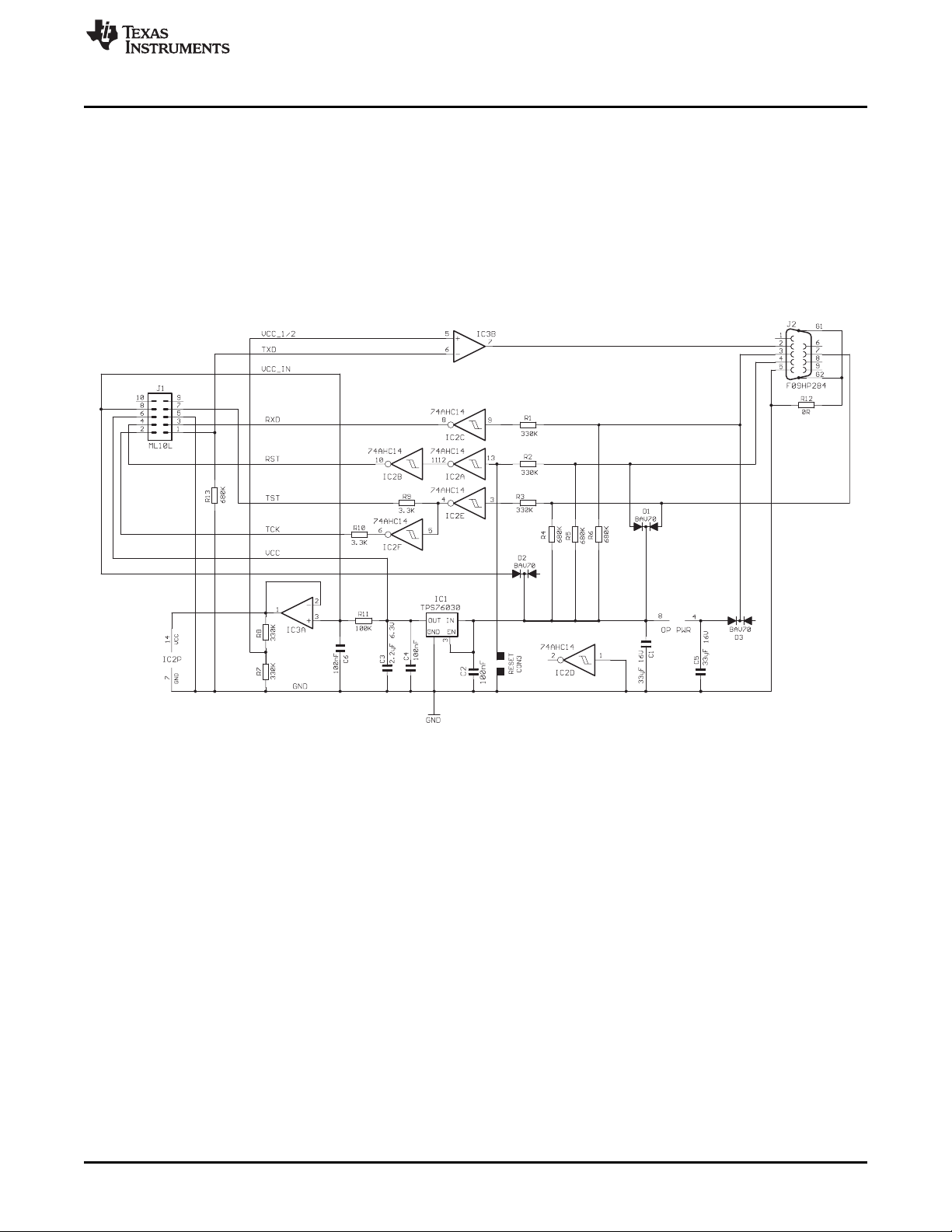
4 Bootloader Hardware
This chapter describes simple and low-cost hardware and software solutions to access the bootloader
functions of the MSP430 flash devices through the serial port (RS-232) of a PC.
4.1 Hardware Description
The low-cost hardware presented in this document (see Figure 3) consists mainly of a low-dropout voltage
regulator, some inverters, and operational amplifiers. There are also some resistors, capacitors, and
diodes. A complete parts list is provided in Section 4.1.4.
The functional blocks are described in more detail in the following sections.
Bootloader Hardware
4.1.1 Power Supply
Power for the bootloader hardware can be supplied from the RS-232 interface. RS-232 signals DTR (pin 7
of the serial connector) and RTS (pin 4 of the serial connector) normally deliver a positive voltage to load
capacitor C1 and power to the low-dropout voltage regulator IC1 (TI TPS76030 or LP2980-3.0, or
equivalent 3-V low-dropout regulator).
Using a fairly big capacitor, it is possible to draw a short-duration current that is higher than the driving
serial port can supply. This feature is required to program the flash memory, for example.
It is also possible to connect an external supply voltage to the hardware on pin 8 of the BSL target
connector (J1). Diodes are used to prevent reverse-polarity flow.
SLAU319S–July 2010–Revised April 2018
Submit Documentation Feedback
Figure 6. Bootloader Interface Schematic
MSP430™ Flash Device Bootloader (BSL)
Copyright © 2010–2018, Texas Instruments Incorporated
29
Bootloader Hardware
4.1.2 Serial Interface
Table 12 shows the signals used to communicate with the bootloader (through connector J2). The names
reflect the pin function as seen from the PC. For example, the PC receives data through the RxD pin,
whereas the bootloader needs to drive this signal.
Pin Name Full Name (PC) 9-Pin SUB-D Function on BSL Interface
RxD Receive data 2 Transmit data to PC
TxD Transmit data 3 Receive data from PC (and negative supply)
DTR Data terminal ready 4 Reset control (and positive supply)
RTS Request to send 7 TEST or TCK control (and positive supply)
GND Ground 5 Ground
4.1.2.1 Level Shifting
Simple CMOS inverters with Schmitt-trigger characteristics (IC2) are used to transform the RS-232 levels
(see Table 13) to CMOS levels.
www.ti.com
Table 12. Serial-Port Signals and Pin Assignments
Table 13. RS-232 Levels
Logic Level RS-232 Level RS-232 Voltage Level
1 Mark –3 V to –15 V
0 Space 3 V to 15 V
The inverters are powered by the operational amplifier IC3A. This amplifier permits adjusting the provided
logic level to the requirements of the connected target application. A voltage applied to pin 8 of the BSL
target connector (VCC_IN) overrides the default 3-V level provided from IC1 and the 100-kΩ series
resistor R11. Thus, the output voltage of the operational amplifier is pulled to the applied voltage VCC_IN.
Depending on the overvoltage protection of the device family selected, the excess voltage is either
conducted to VCC(as in the TI 74HC14) or to GND (as in the TI 74AHC14). If the protection diode
conducts to VCC, the operational amplifier IC3A needs to compensate for the overvoltage. Therefore, TI
recommends the 74AHC14 device, which conducts to ground (GND).
To avoid excessive power dissipation and damage of the protection diodes, series resistors (R1, R2, and
R3) are used to limit the input current.
An operational amplifier (IC3B) is used to generate RS-232 levels out of CMOS levels. The level at the
positive input is set to VCC/2 (1.5 V nominal). If the level at the negative input rises above this level, the
output is pulled to the negative supply of the operational amplifier (mark). If the level drops below VCC/2,
the output is pulled to the positive rail (space).
The positive supply of the operational amplifier is the same as the input to the voltage regulator. A
separate capacitor (C5) is used to generate the negative supply voltage. This capacitor is charged by the
receiving signal of the bootloader hardware (pin 3 on SUB-D connector J2).
During an asynchronous serial communication, the combination of stop bit and start bit is used to
synchronize sender and receiver. After the transmission of a data byte, the stop bit forces the transmission
line into a defined state, which is usually a logic 1 or, in RS-232 terms, a mark. This means that the
transmission-line voltage is negative when there is no transmission and the capacitor can be charged.
Diodes are used to prevent discharge of the capacitor during transmission.
In very rare circumstances, the data sent to the bootloader interface might hold too many zeros, so that
the capacitor C5 required for the negative supply is discharged, causing a malfunction of the interface. (A
possible workaround is to send the data in smaller chunks.) However, under normal operating conditions,
even data that contains all zeros does not cause problems.
30
MSP430™ Flash Device Bootloader (BSL)
Copyright © 2010–2018, Texas Instruments Incorporated
SLAU319S–July 2010–Revised April 2018
Submit Documentation Feedback
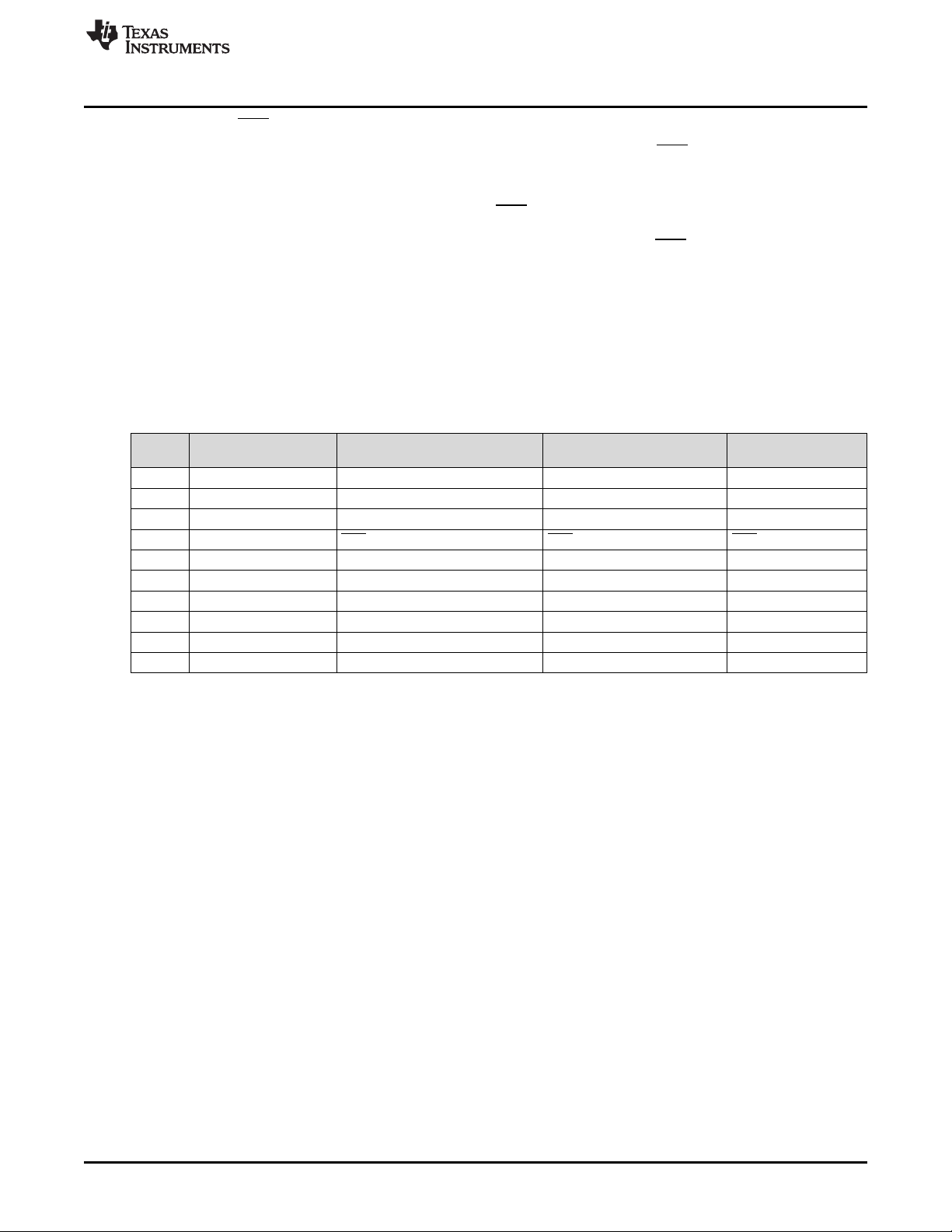
www.ti.com
4.1.2.2 Control of RST/NMI and TEST or TCK Pins
The two pins used to invoke the bootloader software of the MSP430 MCU—RST/NMI and TEST or TCK
(for devices without a dedicated TEST pin)—are controlled by the DTR and RTS signals, respectively.
These signals also deliver a positive voltage to supply the bootloader hardware.
For devices with a dedicated TEST pin, the levels at RST/NMI and TEST during normal operation are
logic 1 and logic 0, respectively. To achieve these levels and to use the corresponding RS-232 signals as
power-supply lines, it is necessary to use two inverters (IC1A, IC2B) for the RST/NMI pin and one inverter
(IC2E) for the TEST pin.
Devices without the TEST pin require the inverted TEST pin sequence on their TCK pin to invoke the
bootloader. Thus, the corresponding signal is inverted (inverter IC2F).
Diodes prevent discharge of capacitor C1 to allow control of the RS-232 lines (RTS and DTR).
4.1.3 Target Connector
Bootloader Hardware
Table 14. Pin Assignment of Target Connector
Pin Signal Name Devices With Test Pin
Pin on MSP430F13x or
MSP430F14x
(1)
Pin on MSP430F4xx
1 TXD P1.1 P1.1 P1.0
2 TCK Do not connect
(2)
TCK TCK
3 RXD P2.2 P2.2 P1.1
4 RST RST/NMI RST/NMI RST/NMI
5 GND GND GND GND
6 VCC(3.0 V) V
(3)
CC
(3)
V
CC
(3)
V
CC
7 TST TEST Do not connect Do not connect
8 VCC_IN V
(3)
CC
(3)
V
CC
(3)
V
CC
9 Not connected — — —
10 Not connected — — —
(1)
For device-specific BSL pin information, see the applicable device data sheet.
(2)
Signal TCK must not be connected on devices with the TEST pin.
(3)
Pin VCC(3.0 V) is a voltage source that can provide a limited current, depending on the serial port driver capability. If an external
power supply is used, VCC(3.0 V) must not be connected to the target. In this case, the external supply voltage must be
connected to pin VCC_IN. Otherwise, VCC_IN must be unconnected.
SLAU319S–July 2010–Revised April 2018
Submit Documentation Feedback
MSP430™ Flash Device Bootloader (BSL)
Copyright © 2010–2018, Texas Instruments Incorporated
31

Bootloader Hardware
4.1.4 Parts List
Table 15 lists the BSL interface parts.
Part Value or Part Number Package Comment
C1 33 µF, 16 V SMD 7243
C2 100 nF SMD 0805
C3 2.2 µF, 6.3 V SMD 1206
C4 100 nF SMD 0805
C5 33 µF, 16 V SMD 7243
C6 100 nF SMD 0805
D1 BAV70 SOT23 High-speed double diode
D2 BAV70 SOT23 High-speed double diode
D3 BAV70 SOT23
IC1 TPS76030 SOT23-5 TI
IC2 74AHC14 SO14 TI
IC3 TL062D SO8 TI
R1 330 kΩ SMD 0805
R2 330 kΩ SMD 0805
R3 330 kΩ SMD 0805
R4 680 kΩ SMD 0805
R5 680 kΩ SMD 0805
R6 680 kΩ SMD 0805
R7 330 kΩ SMD 0805
R8 330 kΩ SMD 0805
R9 3.3 kΩ SMD 0805
R10 3.3 kΩ SMD 0805
R11 100 kΩ SMD 0805
R12 0 kΩ SMD 0805
R13 680 kΩ SMD 0805
J1 Header 2x5 2X05 Target connector (see Table 14)
J2 F09HP284 9-SUB-D female RS-232 connector
CON3 RESET SMD0805 Pads to connect an optional reset button
www.ti.com
Table 15. Universal BSL Interface Parts List
32
MSP430™ Flash Device Bootloader (BSL)
Copyright © 2010–2018, Texas Instruments Incorporated
SLAU319S–July 2010–Revised April 2018
Submit Documentation Feedback

www.ti.com
Differences Between Devices and Bootloader Versions
5 Differences Between Devices and Bootloader Versions
5.1 1xx, 2xx, and 4xx BSL Versions
The tables in this section show the key information of MSP430 device to BSL version assignment related
to their hardware and software resources.
Table 16. BSL Version 1.10 on F13x, F14x(1) (excluding Rev AA), F11x, and F11x1
Device
BSL Version 1.10
BSL vector address
Chip ID address 0FF0h
Chip ID data F149h F112h
BSL version address 0FFAh
BSL version data 0110h
Mass erase time, nominal (ms) 17.2
Read and write access at 0000h to FFFFh Byte
Verification during write (online) No
Stack pointer initialization
Transmit pin (TX), Receive pin (RX) P1.1, P2.2
RAM stack used 0200h to 0219h
Working registers R5 to R9
System clock, affected controls BCSCTL1, DCOCTL
Timer_A, affected controls TACTL, TAR, CCTL0, CCR0
Preparation for software call
Comment 1
Workaround mandatory
Comment 2
Optional for F148, F149 only: Use loadable BSL
(>1 KB RAM required)
Comment 3
Optional for F1x4 to F1x9: Use small loadable BSL
(<512B RAM required)
(1)
To reach the required mass erase time as specified in the data sheet, the mass erase command must be executed several
times.
Cold start 0C00h
Warm start —
SP critical 021Ah
SP not critical Unchanged
Resources Used by BSL
mov #00h, &CCTL0
bic.b #02h, &P1SEL
bic.b #04h, &P2SEL
bic.b #32h, &IE1
mov.b #00h, &BCSCTL2
mov #00h, SR
br &0C00h
Load PATCH.TXT to eliminate ROM bug (see Section 5.2 and
Section 2.5).
Load BL_150S_14x.txt to get all features of V1.60 plus valid
erase segment command (see Section 2.5).
Load BS_150S_14x.txt to get some features of V1.60 (see
Section 2.5).
F13x
F14x(1) up to Rev N
F11x (obsolete)
F11x1 (obsolete)
(1)
SLAU319S–July 2010–Revised April 2018
Submit Documentation Feedback
Copyright © 2010–2018, Texas Instruments Incorporated
MSP430™ Flash Device Bootloader (BSL)
33

Differences Between Devices and Bootloader Versions
Table 17. BSL Version 1.30 on F41x, F11x, and F11x1
www.ti.com
Device F41x
BSL Version 1.30
BSL vector address
Chip ID address 0FF0h
Chip ID data F143h F112h
BSL version address 0FFAh
BSL version data 0130h
Mass erase time, nominal (ms) 206.4
Read and write access at
Verification during write (online) No
Stack pointer initialization
Transmit pin (TX) P1.0 P1.1
Receive pin (RX) P2.1 P2.2
RAM stack used 0200h to 021Fh
Working registers R5 to R9
System clock, affected controls SCFI0, SCFI1, SCFQCTL BCSCTL1, DCOCTL
Timer_A, affected controls TACTL, TAR, CCTL0, CCR0
Preparation for software call
Cold start 0C00h
Warm start 0C02h
0000h to 00FFh Byte
0100h to FFFEh Word
Cold start 0220h
Warm start Unchanged
Resources Used by BSL
mov #00h, &CCTL0
mov.b #00h, &FLLCTL1
br &0C00h
mov #00h, &CCTL0
mov.b #00h, &BCSCTL2
mov #00h, SR
br &0C00h
F11x (obsolete)
F11x1A
34
MSP430™ Flash Device Bootloader (BSL)
SLAU319S–July 2010–Revised April 2018
Submit Documentation Feedback
Copyright © 2010–2018, Texas Instruments Incorporated

www.ti.com
Differences Between Devices and Bootloader Versions
Table 18. BSL Version 1.40 on F12x
Device F122, F123x
BSL Version 1.40
BSL vector address
Chip ID address 0FF0h
Chip ID data F123h
BSL version address 0FFAh
BSL version data 0140h
Mass erase time, nominal (ms) 206.4
Read and write access at
Verification during write (online) For addresses 0200h to FFFEh
Stack pointer initialization
Transmit pin (TX) P1.1
Receive pin (RX) P2.2
RAM stack used 0200h to 021Fh
Working registers R5 to R10
System clock, affected controls BCSCTL1, DCOCTL
Timer_A, affected controls TACTL, TAR, CCTL0, CCR0
Preparation for software call
Cold start 0C00h
Warm start 0C02h
0000h to 00FFh Byte
0100h to FFFEh Word
Cold start 0220h
Warm start Unchanged
Resources Used by BSL
mov.b #00h, &BCSCTL2
mov #00h, SR
br &0C00h
SLAU319S–July 2010–Revised April 2018
Submit Documentation Feedback
Copyright © 2010–2018, Texas Instruments Incorporated
MSP430™ Flash Device Bootloader (BSL)
35

Differences Between Devices and Bootloader Versions
Table 19. BSL Version 1.60 on F11x2, F12x2, F43x, F44x, FE42x, FW42x, F43x, FG43x, F415, F417
www.ti.com
Device
BSL Version 1.60
BSL vector address
Chip ID address 0FF0h
Chip ID data 1132h 1232h F449h F427h F439h
BSL version address 0FFAh
BSL version data 0160h
Mass erase time, nominal (ms) 206.4
Read and write access at
Verification during write (online) For addresses 0200h to FFFEh
Erase check command Yes (error address 0200h)
Erase segment command With erasure verification (error address 0200h)
TX identification command Yes
Change baud rate command Yes
Stack pointer initialization
Transmit pin (TX) P1.1 P1.0
Receive pin (RX) P2.2 P1.1
RAM stack used 0200h to 021Fh
Working registers R5 to R12
System clock, affected controls BCSCTL1, DCOCTL SCFI0, SCFI1, SCFQCTL
Timer_A, affected controls TACTL, TAR, CCTL0, CCR0
Preparation for software call
Comment
Cold start 0C00h
Warm start 0C02h
0000h to 00FFh Byte
0100h to FFFEh Word
Cold start 0220h
Warm start Unchanged
Erase segment
command
F1122,
F1132
Resources Used by BSL
mov.b #00h, &BCSCTL2
mov #00h, SR
br &0C00h
Addresses 1000h to 11FFh are verified coherently (three segments). Also use erase
check command.
F1222,
F1232
F43x,
F44x
mov.b #00h, &FLLCTL1
br &0C00h
FE42x,
FW42x,
F415,
F417
F43x,
FG43x
36
MSP430™ Flash Device Bootloader (BSL)
SLAU319S–July 2010–Revised April 2018
Submit Documentation Feedback
Copyright © 2010–2018, Texas Instruments Incorporated

www.ti.com
Table 20. BSL Version 1.61 on F16x, F161x, F42x0, F13x rev AA, F14x(1) rev AA, F47x, FG47x
Differences Between Devices and Bootloader Versions
Device F16x F161x
BSL Version 1.61
BSL vector address
Chip ID address 0FF0h
Chip ID data 0F169h 0F16Ch F149h F427h 4152h F47Fh 0F479h
BSL version address 0FFAh
BSL version data 0161h
Mass erase time, nominal (ms) 206.4
Read and write access at
Verification during write (online) For addresses 0200h to FFFEh
Erase check command Yes (error address 0200h)
Erase segment command With erasure verification (error address 0200h)
TX identification command Yes
Change baud rate command Yes
Stack pointer initialization
Transmit pin (TX) P1.1 P1.0
Receive pin (RX) P2.2 P1.1
RAM stack used 0200h to 021Fh
Working registers R5 to R14
System clock, affected controls BCSCTL1, DCOCTL SCFI0, SCFI1, SCFQCTL
Timer_A, affected controls TACTL, TAR, CCTL0, CCR0
Preparation for software call
Comment
Cold start 0C00h
Warm start 0C02h
0000h to 00FFh Byte
0100h to FFFEh Word
Cold start 0220h
Warm start Unchanged
Resources Used by BSL
mov.b #00h, &BCSCTL2
mov #00h, SR
br &0C00h
Erase segment
command
Addresses 1000h to 11FFh are verified coherently (three segments). Also use erase
check command.
F149
Rev AA
F42x0 F41x2 F47197 FG47x
mov.b #00h, &FLLCTL1
br &0C00h
SLAU319S–July 2010–Revised April 2018
Submit Documentation Feedback
Copyright © 2010–2018, Texas Instruments Incorporated
MSP430™ Flash Device Bootloader (BSL)
37
Differences Between Devices and Bootloader Versions
www.ti.com
Table 21. BSL Version 2.02 and 2.13 on F21xx, F22xx, F23xx, F24xx, F261x
Device F21xx F22xx F23xx F24x F261x
BSL Version 2.02 2.13
BSL Vector Address
Chip ID Address 0FF0h
Chip ID Data F213h F227h F237h F249h F26Fh
BSL Version Address 0FFAh
BSL Version Data 0202h 0213h
Read and Write Access at
Verification during write (online) For addresses 0200h to FFFEh
Erase Check Command Yes (error address 0200h)
Erase Segment Command With erasure verification (error address 0200h)
TX Identification command Yes
Change baud rate command Yes
Stack Pointer Initialization
Transmit Pin (TX) P1.1
Receive Pin (RX) P2.2
RAM Stack Used 0200h to 021Fh 0200h to 0223h
Working Registers R5 to R14 R4 to R15
System clock, affected controls BCSCTL1, DCOCTL
Timer_A, Affected controls TACTL, TAR, CCTL0, CCR0
Preparation for software call
Comment
(1)
The LOCK and LOCKA bits must be cleared by the user application before entering the BSL:
mov.w #FWKEY+LOCKA,&FCTL3
Cold Start 0C00h
Warm Start 0C02h
(1)
0000h to 00FFh Byte
0100h to FFFEh Word
Cold Start 0220h 0224h
Warm Start Unchanged
Resources Used by BSL
SCFI0, SCFI1,
SCFQCTL
mov.b #00h, &BCSCTL2
mov #00h, SR
br &0C00h
Erase Segment
Command
Addresses 1000h to 11FFh are verified coherently (five segments). Also use erase
check command.
38
MSP430™ Flash Device Bootloader (BSL)
SLAU319S–July 2010–Revised April 2018
Submit Documentation Feedback
Copyright © 2010–2018, Texas Instruments Incorporated

www.ti.com
Table 22. BSL Version 2.02 and 2.03 on G2xx3, G2xx4, G2xx5, TCH5E
Differences Between Devices and Bootloader Versions
(1)
Device G2xx4 G2xx5 G2xx3 TCH5E
BSL Version 2.02 2.03
BSL Vector Address
Cold Start 0C00h
Warm Start 0C02h
(2)
Chip ID Address 0FF0h
Chip ID Data F227h 2955h 2553h 255Ch
BSL Version Address 0FFAh
BSL Version Data 0202h 0203h
Read and Write Access at
0000h to 00FFh Byte
0100h to FFFEh Word
Verification during write (online) For addresses 0200h to FFFEh
Erase Check Command Yes (error address 0200h)
Erase Segment Command With erasure verification (error address 0200h)
TX Identification command Yes
Change baud rate command Yes
Stack Pointer Initialization
Cold Start 0220h
Warm Start Unchanged
Resources Used by BSL
Transmit Pin (TX) P1.1 P1.1
Receive Pin (RX) P2.2 P1.5
RAM Stack Used 0200h to 021Fh
Working Registers R5 to R14
System clock, affected controls BCSCTL1, DCOCTL
Timer_A, Affected controls TACTL, TAR, CCTL0, CCR0
mov.b #00h, &BCSCTL2
Preparation for software call
mov #00h, SR
br &0C00h
Comment
(1)
Not all Value Line devices contain a BSL; see device-specific data sheet.
(2)
The LOCK and LOCKA bits must be cleared by the user application before entering the BSL:
Erase Segment
Command
Addresses 1000h to 11FFh are verified coherently (five segments). Also use
erase check command.
mov.w #FWKEY+LOCKA,&FCTL3
SLAU319S–July 2010–Revised April 2018
Submit Documentation Feedback
Copyright © 2010–2018, Texas Instruments Incorporated
MSP430™ Flash Device Bootloader (BSL)
39

Differences Between Devices and Bootloader Versions
Table 23. BSL Version 2.12 and 2.13 on FG46xx, F471xx
Device FG46xx F471xx
BSL Version 2.12 2.13
BSL vector address
Chip ID address 0FF0h
Chip ID data F46Fh
BSL version address 0FFAh
BSL version data 0212h 0213h
Mass erase time, nominal (ms) 206.4
Read and write access at
Verification during write (online) For addresses 0200h to FFFEh
Erase check command Yes (error address 0200h)
Erase segment command
TX identification command Yes
Change baud rate command Yes
Stack pointer initialization
Transmit pin (TX) P1.0
Receive pin (RX) P1.1
RAM stack used 0200h to 0223h
Working registers R4 to R15
System clock, affected controls SCFI0, SCFI1, SCFQCTL
Timer_A, affected controls TACTL, TAR, CCTL0, CCR0
Preparation for software call
Comment Erase segment command
(1)
The LOCK and LOCKA bits must be cleared by the user application before entering the BSL:
mov.w #FWKEY+LOCKA,&FCTL3.
Cold start 0C00h
Warm start 0C02h
0000h to 00FFh Byte
0100h to FFFEh Word
Erase segment command with erasure verification (error address
Cold start 0224h
Warm start Unchanged
Resources Used by BSL
mov.b #00h, &FLLCTL1
br &0C00h
Addresses 1000h to 11FFh are verified coherently (five segments).
Also use erase check command.
(1)
0200h)
www.ti.com
5.2 Special Consideration for ROM BSL Version 1.10
The first official version V1.10 of the ROM BSL requires a small loadable patch sequence, PATCH.TXT, to
reliably execute the RX block command. The same procedure must be executed if a loadable BSL is
downloaded to such a device. After the BSL has been started, proceed in the following manner:
1. RX password (unlock password protection for the following command)
2. Load program counter (PC) with 0C22h (initialize stack pointer to a safe address)
3. RX password again (unlock password protection for subsequent commands)
4. RX data block (code of loadable patch, code section address is 0220h)
5. TX data block (code of loadable patch for verification)
From this time forward, the RX block and TX block commands can be used with one restriction: prior to
their invocation, the program counter must be set to the start address of the patch.
1. Load program counter (PC) with start address 0220h of loadable patch
2. RX data block (code to be programmed at any location), or
3. TX data block (from any location)
40
MSP430™ Flash Device Bootloader (BSL)
Copyright © 2010–2018, Texas Instruments Incorporated
SLAU319S–July 2010–Revised April 2018
Submit Documentation Feedback

www.ti.com
Differences Between Devices and Bootloader Versions
5.3 1xx, 2xx, and 4xx BSL Known Issues
BSL Command Erase Main or Info
Versions Affected 1.x
Description Does not erase information memory when supplied with address in information memory
Workarounds Use Erase Segment command
BSL Command Erase Main or Info
Versions Affected 1.x
Description
Workarounds Use any other main memory address
BSL Command Erase Segment
Versions Affected 1.x
Description Reports failure when used in information memory. However, the erase is properly performed.
Workarounds None
Reports failure when first segment of code memory is supplied as address. However, the erase is
properly performed.
5.4 Special Note on the MSP430F14x Device Family BSL
Revision AA of the MSP430F14x devices have a BSL that was updated to Version 1.61. The primary
reasons for this change were to increase IP security, ensure correct flash programming and mass erase,
and to negate the need for using any patches during programming. To ensure a smooth transition, a
programming environment should be updated to take into account the following changes:
• The Mass Erase command needs to be issued only once, and execution of this command takes
longer.
• Only word writes are allowed to flash memory.
• No patch or RAM loadable BSL is required.
• BSL has "online verification" to speed programming.
• Memory allocation has changed (see BSL version charts in Section 5.3).
• BSL can return a NAK if Segment Erase fails.
• Transmit BSL Version and Change Baud rate are now unprotected.
SLAU319S–July 2010–Revised April 2018
Submit Documentation Feedback
MSP430™ Flash Device Bootloader (BSL)
Copyright © 2010–2018, Texas Instruments Incorporated
41
Differences Between Devices and Bootloader Versions
www.ti.com
5.5 F5xx and F6xx Flash-Based BSL Versions
Table 24.
Devices MSP430F5438, MSP430F5437, MSP430F5435, MSP430F5436, MSP430F5435, MSP430F5419, MSP430F5418
BSL Version 00.01.01.01
RAM Erased None
Buffer Size for Core
Commands
Notable Information
Known Bugs
260 bytes
1. UART TX and RX BSL pins are noted in the device data sheet
2. The BSL does not contain a mechanism to unlock the BSL area for erasing and writing a custom BSL.
3. This function is not supported in this version. The BSL may be safely erased however.
4. The only supported baud rates are 9600 and 57600.
5. The BSL transmits on TA0.0 and receives on TA0.1.
6. The BSL does not expect a parity bit.
1. The password for the BSL is the bytes between addresses 0xFFF0 and 0xFFFF. This means that this BSL
version expects only 16 bytes for a password in the RX Password command. Sending 32 bytes returns an
error.
2. If the address 0x20396 or 0x20397 is included in the address range of the CRC command, the returned data is
incorrect.
3. The Mass Erase command also erases Info_A.
4. On incorrect password, the device erases all RAM, including its stack. Thus, proper return of an error code is
not assured.
5. The total number of bytes for the CRC function is masked with 0x7FFF and is, therefore, limited to 32767.
Devices
BSL Version
RAM Erased 0x1C00 to 0x5BFF
Buffer Size for Core
Commands
Notable Information
Known Bugs
Devices
BSL Version
RAM Erased 0x1C00 to 0x23FF
Buffer Size for Core
Commands
Notable Information
Known Bugs
MSP430F5438A, MSP430F5437A, MSP430F5435A, MSP430F5436A, MSP430F5435A, MSP430F5419A,
MSP430F5418A
00.05.04.03 (Rev A to Rev E)
00.07.05.04 (Rev F and later)
260 bytes
1. UART TX and RX BSL pins are noted in the device data sheet
1. The baud rate of 115k cannot be ensured across all clock, voltage, and temperature variations.
CC430F6147, CC430F6145, CC430F6143, CC430F6137, CC430F6135, CC430F6127, CC430F6126,
CC430F6125, CC430F5147, CC430F5145, CC430F5143, CC430F5137, CC430F5135, CC430F5133,
CC430F5125, CC430F5123
00.05.04.52 (Rev A to Rev C)
00.07.05.53 (Rev D and later)
260 bytes
1. UART TX and RX BSL pins are implemented on pin P1.6 (TXD) and P1.5 (RXD)
1. The baud rate of 115k cannot be ensured across all clock, voltage, and temperature variations.
Table 25.
Table 26.
42
MSP430™ Flash Device Bootloader (BSL)
Copyright © 2010–2018, Texas Instruments Incorporated
SLAU319S–July 2010–Revised April 2018
Submit Documentation Feedback

www.ti.com
Differences Between Devices and Bootloader Versions
Table 27.
Devices
BSL Version
RAM Erased 0x2400 to 0x33FF
Buffer Size for Core
Commands
Notable Information
Known Bugs The USB module is not correctly locked by the BSL. For legacy reasons this behavior is kept.
MSP430F5510, MSP430F5500, MSP430F5501, MSP430F5502, MSP430F5503, MSP430F5504, MSP430F5505,
MSP430F5506, MSP430F5507, MSP430F5508, MSP430F5509
00.03.83.33 (Rev A to Rev E)
00.07.88.38 (Rev F until May 2015)
00.08.88.39 (Rev F and later)
62 bytes
1. Device is programmed with the factory USB BSL.
2. Factory USB BSL is RAM write only. Full BSL must first be loaded into device RAM and started to perform
flash write. Only the commands RX PASSWORD, RX DATA BLOCK FAST, and SET PC are supported.
3. When starting this BSL from an application, the application should first de-enumerate itself, then delay
(approximately 500 ms) before starting the BSL. This allows proper re-enumeration with the host.
4. External crystal at XT2 is required to ensure USB operation.
Table 28.
Devices
BSL Version
RAM Erased 0x2400 to 0x33FF
Buffer Size for Core
Commands
Notable Information
Known Bugs The USB module is not correctly locked by the BSL. For legacy reasons this behavior is kept.
MSP430F5529, MSP430F5513, MSP430F5514, MSP430F5515, MSP430F5517, MSP430F5519, MSP430F5521,
MSP430F5522, MSP430F5524, MSP430F5525, MSP430F5526, MSP430F5527, MSP430F5528
00.03.83.33 (Rev A to Rev H)
00.07.85.36 (Rev I)
00.07.87.37 (Rev J)
00.07.88.38 (Rev K until May 2015)
00.08.88.39 (Rev K and later)
62 bytes
1. Device is programmed with the factory USB BSL.
2. Factory USB BSL is RAM write only. Full BSL must first be loaded into device RAM and started to perform
flash write. Only the commands RX PASSWORD, RX DATA BLOCK FAST, and SET PC are supported.
3. When starting this BSL from an application, the application should first de-enumerate itself, then delay
(approximately 500 ms) before starting the BSL. This allows proper re-enumeration with the host.
4. External crystal at XT2 is required to ensure USB operation.
Table 29.
Devices MSP430F5172, MSP430F5152, MSP430F5132, MSP430F5171, MSP430F5151, MSP430F5131
BSL Version 00.07.05.04
RAM Erased 0x1C00 to 0x1FFF
Buffer Size for Core
Commands
Notable Information
Known Bugs
SLAU319S–July 2010–Revised April 2018
Submit Documentation Feedback
260 bytes
1. UART TX and RX BSL pins are noted in the device data sheet
1. The baud rate of 115k cannot be ensured across all clock, voltage, and temperature variations.
MSP430™ Flash Device Bootloader (BSL)
Copyright © 2010–2018, Texas Instruments Incorporated
43

Differences Between Devices and Bootloader Versions
www.ti.com
Table 30.
Devices
BSL Version 00.07.05.04
RAM Erased 0x2400 to 0x43FF
Buffer Size for Core
Commands
Notable Information
Known Bugs
MSP430F5229, MSP430F5227, MSP430F5219, MSP430F5217, MSP430F5224, MSP430F5222, MSP430F5213,
MSP430F5212
260 bytes
1. UART TX and RX BSL pins are noted in the device data sheet
1. The baud rate of 115k cannot be ensured across all clock, voltage, and temperature variations.
Table 31.
Devices
BSL Version 00.08.08.04
RAM Erased 0x2400 to 0x43FF
Buffer Size for Core
Commands
Notable Information
Known Bugs
MSP430F5249, MSP430F5247, MSP430F5244, MSP430F5242, MSP430F5239, MSP430F5237, MSP430F5234,
MSP430F5232
260 bytes
1. UART TX and RX BSL pins are noted in the device data sheet
1. The baud rate of 115k cannot be ensured across all clock, voltage, and temperature variations.
Table 32.
Devices MSP430F5255, MSP430F5254, MSP430F5253, MSP430F5252
BSL Version 00.08.08.04
RAM Erased 0x2400 to 0x43FF
Buffer Size for Core
Commands
Notable Information
Known Bugs
260 bytes
1. UART TX and RX BSL pins are noted in the device data sheet
2. A BSL firmware image that uses pins in the DVIO supply domain is available for download in the custom BSL
package.
1. The baud rate of 115k cannot be ensured across all clock, voltage, and temperature variations.
Table 33.
Devices MSP430F5259, MSP430F5258, MSP430F5257, MSP430F5256
BSL Version 00.07.06.94
RAM erased 0x1C00 to 0x23FF
Buffer size for Core
Commands
Notable Information
Known Bugs
44
MSP430™ Flash Device Bootloader (BSL)
260 bytes
1. I2C pins are noted in the device data sheet
1. I2C read commands with length greater than 260 do not return correct data.
Copyright © 2010–2018, Texas Instruments Incorporated
SLAU319S–July 2010–Revised April 2018
Submit Documentation Feedback
www.ti.com
Differences Between Devices and Bootloader Versions
Table 34.
Devices
BSL Version 00.06.04.04
RAM Erased 0x1C00 to 0x33FF
Buffer Size for Core
Commands
Notable Information
Known Bugs
MSP430F5310, MSP430F5309, MSP430F5308, MSP430F5304, MSP430F5340, MSP430F5341, MSP430F5342,
MSP430F5329, MSP430F5324, MSP430F5325, MSP430F5326, MSP430F5327, MSP430F5328
260 bytes
1. UART TX and RX BSL pins are noted in the device data sheet
1. The baud rate of 115k cannot be ensured across all clock, voltage, and temperature variations.
Table 35.
Devices
BSL Version
RAM erased 0x2400 to 0x33FF
Buffer Size for Core
Commands
Notable Information
Known Bugs The USB module is not correctly locked by the BSL. For legacy reasons this behavior is kept.
MSP430F6638, MSP430F6637, MSP430F6636, MSP430F6635, MSP430F6634, MSP430F6633, MSP430F6632,
MSP430F6631, MSP430F6630, MSP430F5638, MSP430F5637, MSP430F5636, MSP430F5635, MSP430F5634,
MSP430F5633, MSP430F5632, MSP430F5631, MSP430F5630
00.04.84.34 (Rev A to Rev D)
00.08.88.38 (Rev E until May 2015)
00.08.88.39 (Rev E and later)
62 bytes
1. Device is programmed with the factory USB BSL.
2. Factory USB BSL is RAM write only. Full BSL must first be loaded into device RAM and started to perform
flash write. Only the commands RX PASSWORD, RX DATA BLOCK FAST, and SET PC are supported
3. When starting this BSL from an application, the application should first de-enumerate itself, then delay
(approximately 500 ms) before starting the BSL. This allows proper re-enumeration with the host.
Table 36.
Devices MSP430F6659, MSP430F6658, MSP430F5659, MSP430F5658
BSL Version
RAM Erased 0x2400 to 0x33FF
Buffer Size for Core
Commands
Notable Information
Known Bugs
00.07.86.36 (Rev A)
00.08.88.38 (Rev B until May 2015)
00.08.88.39 (Rev B and later)
62 bytes
1. Device is programmed with the factory USB BSL.
2. Factory USB BSL is RAM write only. Full BSL must first be loaded into device RAM and started to perform
flash write. Only the commands RX PASSWORD, RX DATA BLOCK FAST, and SET PC are supported
3. When starting this BSL from an application, the application should first de-enumerate itself, then delay
(approximately 500 ms) before starting the BSL. This allows proper re-enumeration with the host.
Table 37.
Devices
BSL Version 00.07.05.04
RAM Erased 0x1C00 to 0x43FF
Buffer Size for Core
Commands
Notable Information
Known Bugs
MSP430F6438, MSP430F6436, MSP430F6435, MSP430F6433, MSP430F5338, MSP430F5336, MSP430F5335,
MSP430F5333, MSP430F6459, MSP430F6458, MSP430F5359, MSP430F5358
260 bytes
1. UART TX and RX BSL pins are noted in the device data sheet
1. The baud rate of 115k cannot be ensured across all clock, voltage, and temperature variations.
SLAU319S–July 2010–Revised April 2018
Submit Documentation Feedback
MSP430™ Flash Device Bootloader (BSL)
Copyright © 2010–2018, Texas Instruments Incorporated
45
Differences Between Devices and Bootloader Versions
MSP430F6736, MSP430F6720, MSP430F6721, MSP430F6723, MSP430F6724, MSP430F6725, MSP430F6726,
Devices
BSL Version 00.07.05.04
RAM Erased 0x1C00 to 0x1FFF
Buffer Size for Core
Commands
Notable Information
Known Bugs
Devices
BSL Version 00.07.05.04
RAM Erased 0x1C00 to 0x5BFF
Buffer Size for Core
Commands
Notable Information
Known Bugs
MSP430F6730, MSP430F6731, MSP430F6733, MSP430F6734, MSP430F6735, MSP430F6736A,
MSP430F6735A, MSP430F6734A, MSP430F6733A, MSP430F6731A, MSP430F6730A, MSP430F6726A,
MSP430F6725A, MSP430F6724A, MSP430F6723A, MSP430F6721A, MSP430F6720A
260 bytes
1. UART TX and RX BSL pins are noted in the device data sheet
1. The baud rate of 115k cannot be ensured across all clock, voltage, and temperature variations.
MSP430F6779, MSP430F6745, MSP430F6746, MSP430F6747, MSP430F6748, MSP430F6749, MSP430F6765,
MSP430F6776, MSP430F6767, MSP430F6768, MSP430F6769, MSP430F6775, MSP430F6776, MSP430F6777,
MSP430F6778, MSP430F67791, MSP430F67451, MSP430F67461, MSP430F67471, MSP430F67481,
MSP430F67491, MSP430F67651, MSP430F67761, MSP430F67671, MSP430F67681, MSP430F67691,
MSP430F67751, MSP430F67761, MSP430F67771, MSP430F67781
260 bytes
1. UART TX and RX BSL pins are noted in the device data sheet
1. The baud rate of 115k cannot be ensured across all clock, voltage, and temperature variations.
www.ti.com
Table 38.
Table 39.
MSP430F6779A, MSP430F6778A, MSP430F6777A, MSP430F6776A, MSP430F6775A, MSP430F6769A,
Devices
BSL Version 00.07.05.04
RAM Erased 0x1C00 to 0x5BFF
Buffer Size for Core
Commands
Notable Information
Known Bugs
Devices MSP430F67641, MSP430F67621
BSL Version 00.07.05.04
RAM Erased 0x1C00 to 0x1FFF
Buffer Size for Core
Commands
Notable Information
Known Bugs
MSP430F6768A, MSP430F6767A, MSP430F6766A, MSP430F6765A MSP430F6749A, MSP430F6748A,
MSP430F6747A MSP430F6746A MSP430F6745A, MSP430F67791A, MSP430F67781A, MSP430F67771A,
MSP430F67761A, MSP430F67751A, MSP430F67691A, MSP430F67681A, MSP430F67671A, MSP430F67661A,
MSP430F67651A, MSP430F67491A, MSP430F67481A, MSP430F67471A, MSP430F67461A, MSP430F67451A
260 bytes
1. UART TX and RX BSL pins are noted in the device data sheet
1. The baud rate of 115k cannot be ensured across all clock, voltage, and temperature variations.
260 bytes
1. UART TX and RX BSL pins are noted in the device data sheet
1. The baud rate of 115k cannot be ensured across all clock, voltage, and temperature variations.
Table 40.
Table 41.
46
MSP430™ Flash Device Bootloader (BSL)
Copyright © 2010–2018, Texas Instruments Incorporated
SLAU319S–July 2010–Revised April 2018
Submit Documentation Feedback
www.ti.com
Devices MSP430FG6426, MSP430FG6425
BSL Version 00.08.08.04
RAM Erased 0x1C00 to 0x43FF
Buffer Size for Core
Commands
Notable Information
Known Bugs
Devices MSP430FG6626, MSP430FG6625
BSL Version 00.08.88.38
RAM Erased 0x1C00 to 0x43FF
Buffer Size for Core
Commands
Notable Information
Known Bugs
260 bytes
1. UART TX and RX BSL pins are noted in the device data sheet
1. The baud rate of 115k cannot be ensured across all clock, voltage, and temperature variations.
260 bytes
1. Device is programmed with the factory USB BSL.
2. Factory USB BSL is RAM write only. Full BSL must first be loaded into device RAM and started to perform
flash write. Only the commands RX PASSWORD, RX DATA BLOCK FAST, and SET PC are supported
3. When starting this BSL from an application, the application should first de-enumerate itself, then delay
(approximately 500 ms) before starting the BSL. This allows proper re-enumeration with the host.
4. External crystal at XT2 is required to ensure USB operation.
Differences Between Devices and Bootloader Versions
Table 42.
Table 43.
SLAU319S–July 2010–Revised April 2018
Submit Documentation Feedback
MSP430™ Flash Device Bootloader (BSL)
Copyright © 2010–2018, Texas Instruments Incorporated
47

unibottom.wmf@
unitop.wmf@
Bootloader PCB Layout Suggestion
6 Bootloader PCB Layout Suggestion
Figure 7. Universal BSL Interface PCB Layout, Top
www.ti.com
48
Figure 8. Universal BSL Interface PCB Layout, Bottom
MSP430™ Flash Device Bootloader (BSL)
Copyright © 2010–2018, Texas Instruments Incorporated
SLAU319S–July 2010–Revised April 2018
Submit Documentation Feedback

3,5 mm
60,00 mm
www.ti.com
Bootloader PCB Layout Suggestion
Figure 9. Universal BSL Interface Component Placement
SLAU319S–July 2010–Revised April 2018
Submit Documentation Feedback
MSP430™ Flash Device Bootloader (BSL)
Copyright © 2010–2018, Texas Instruments Incorporated
49

3,5 mm
60,0 mm
TL062D
Bootloader PCB Layout Suggestion
www.ti.com
50
Figure 10. Universal BSL Interface Component Placement
MSP430™ Flash Device Bootloader (BSL)
Copyright © 2010–2018, Texas Instruments Incorporated
SLAU319S–July 2010–Revised April 2018
Submit Documentation Feedback

www.ti.com
Revision History
Revision History
NOTE: Page numbers for previous revisions may differ from page numbers in the current version.
Changes from March 7, 2018 to April 12, 2018 ............................................................................................................... Page
• Added item (1) to Notable Information in Table 24.................................................................................. 42
• Updated item (1) in Notable Information in Table 25 ............................................................................... 42
• Updated item (1) in Notable Information in Table 26 ............................................................................... 42
• Added item (1) and updated item (2) in Notable Information in Table 27........................................................ 43
• Added item (1) and updated item (2) in Notable Information in Table 28........................................................ 43
• Updated item (1) in Notable Information in Table 29 ............................................................................... 43
• Updated item (1) in Notable Information in Table 30 ............................................................................... 44
• Updated item (1) in Notable Information in Table 31 ............................................................................... 44
• Updated item (1) in Notable Information in Table 32 ............................................................................... 44
• Updated item (1) in Notable Information in Table 34 ............................................................................... 45
• Added item (1) and updated item (2) in Notable Information in Table 35........................................................ 45
• Added item (1) and updated item (2) in Notable Information in Table 36........................................................ 45
• Updated item (1) in Notable Information in Table 37 ............................................................................... 45
• Updated item (1) in Notable Information in Table 38 ............................................................................... 46
• Updated item (1) in Notable Information in Table 39 ............................................................................... 46
• Updated item (1) in Notable Information in Table 40 ............................................................................... 46
• Updated item (1) in Notable Information in Table 41 ............................................................................... 46
• Updated item (1) in Notable Information in Table 42 ............................................................................... 47
• Added all items in Notable Information in Table 43 ................................................................................. 47
SLAU319S–July 2010–Revised April 2018
Submit Documentation Feedback
Copyright © 2010–2018, Texas Instruments Incorporated
Revision History
51

IMPORTANT NOTICE FOR TI DESIGN INFORMATION AND RESOURCES
Texas Instruments Incorporated (‘TI”) technical, application or other design advice, services or information, including, but not limited to,
reference designs and materials relating to evaluation modules, (collectively, “TI Resources”) are intended to assist designers who are
developing applications that incorporate TI products; by downloading, accessing or using any particular TI Resource in any way, you
(individually or, if you are acting on behalf of a company, your company) agree to use it solely for this purpose and subject to the terms of
this Notice.
TI’s provision of TI Resources does not expand or otherwise alter TI’s applicable published warranties or warranty disclaimers for TI
products, and no additional obligations or liabilities arise from TI providing such TI Resources. TI reserves the right to make corrections,
enhancements, improvements and other changes to its TI Resources.
You understand and agree that you remain responsible for using your independent analysis, evaluation and judgment in designing your
applications and that you have full and exclusive responsibility to assure the safety of your applications and compliance of your applications
(and of all TI products used in or for your applications) with all applicable regulations, laws and other applicable requirements. You
represent that, with respect to your applications, you have all the necessary expertise to create and implement safeguards that (1)
anticipate dangerous consequences of failures, (2) monitor failures and their consequences, and (3) lessen the likelihood of failures that
might cause harm and take appropriate actions. You agree that prior to using or distributing any applications that include TI products, you
will thoroughly test such applications and the functionality of such TI products as used in such applications. TI has not conducted any
testing other than that specifically described in the published documentation for a particular TI Resource.
You are authorized to use, copy and modify any individual TI Resource only in connection with the development of applications that include
the TI product(s) identified in such TI Resource. NO OTHER LICENSE, EXPRESS OR IMPLIED, BY ESTOPPEL OR OTHERWISE TO
ANY OTHER TI INTELLECTUAL PROPERTY RIGHT, AND NO LICENSE TO ANY TECHNOLOGY OR INTELLECTUAL PROPERTY
RIGHT OF TI OR ANY THIRD PARTY IS GRANTED HEREIN, including but not limited to any patent right, copyright, mask work right, or
other intellectual property right relating to any combination, machine, or process in which TI products or services are used. Information
regarding or referencing third-party products or services does not constitute a license to use such products or services, or a warranty or
endorsement thereof. Use of TI Resources may require a license from a third party under the patents or other intellectual property of the
third party, or a license from TI under the patents or other intellectual property of TI.
TI RESOURCES ARE PROVIDED “AS IS” AND WITH ALL FAULTS. TI DISCLAIMS ALL OTHER WARRANTIES OR
REPRESENTATIONS, EXPRESS OR IMPLIED, REGARDING TI RESOURCES OR USE THEREOF, INCLUDING BUT NOT LIMITED TO
ACCURACY OR COMPLETENESS, TITLE, ANY EPIDEMIC FAILURE WARRANTY AND ANY IMPLIED WARRANTIES OF
MERCHANTABILITY, FITNESS FOR A PARTICULAR PURPOSE, AND NON-INFRINGEMENT OF ANY THIRD PARTY INTELLECTUAL
PROPERTY RIGHTS.
TI SHALL NOT BE LIABLE FOR AND SHALL NOT DEFEND OR INDEMNIFY YOU AGAINST ANY CLAIM, INCLUDING BUT NOT
LIMITED TO ANY INFRINGEMENT CLAIM THAT RELATES TO OR IS BASED ON ANY COMBINATION OF PRODUCTS EVEN IF
DESCRIBED IN TI RESOURCES OR OTHERWISE. IN NO EVENT SHALL TI BE LIABLE FOR ANY ACTUAL, DIRECT, SPECIAL,
COLLATERAL, INDIRECT, PUNITIVE, INCIDENTAL, CONSEQUENTIAL OR EXEMPLARY DAMAGES IN CONNECTION WITH OR
ARISING OUT OF TI RESOURCES OR USE THEREOF, AND REGARDLESS OF WHETHER TI HAS BEEN ADVISED OF THE
POSSIBILITY OF SUCH DAMAGES.
You agree to fully indemnify TI and its representatives against any damages, costs, losses, and/or liabilities arising out of your noncompliance with the terms and provisions of this Notice.
This Notice applies to TI Resources. Additional terms apply to the use and purchase of certain types of materials, TI products and services.
These include; without limitation, TI’s standard terms for semiconductor products http://www.ti.com/sc/docs/stdterms.htm), evaluation
modules, and samples (http://www.ti.com/sc/docs/sampterms.htm).
Mailing Address: Texas Instruments, Post Office Box 655303, Dallas, Texas 75265
Copyright © 2018, Texas Instruments Incorporated
 Loading...