


JM38510-65761BRA
Texas Instruments JM38510-65761BRA, SN54HCT541J, SN74HCT541DBR, SN74HCT541DW, SN74HCT541DWR Datasheet
...
SN54HCT541, SN74HCT541
OCTAL BUFFERS AND LINE DRIVERS
WITH 3-STATE OUTPUTS
SCLS306A – JANUARY 1996 – REVISED MA Y 1997
1
POST OFFICE BOX 655303 • DALLAS, TEXAS 75265
D
Inputs Are TTL-Voltage Compatible
D
High-Current 3-State Outputs Interface
Directly With System Bus or Can Drive up
to 15 LSTTL Loads
D
Data Flow-Through Pinout (All Inputs on
Opposite Side From Outputs)
D
Package Options Include Plastic
Small-Outline (DW) and Ceramic Flat (W)
Packages, Ceramic Chip Carriers (FK), and
Standard Plastic (N) and Ceramic (J)
300-mil DIPs
description
These octal buffers and line drivers are designed
to have the performance of the popular ’HC240
series and to offer a pinout with inputs and outputs
on opposite sides of the package. This
arrangement greatly facilitates printed circuit
board layout.
The 3-state control gate is a 2-input NOR. If either
output-enable (OE1
or OE2) input is high, all eight
outputs are in the high-impedance state. The
’HCT541 provide true data at the outputs.
The SN54HCT541 is characterized for operation
over the full military temperature range of –55°C
to 125°C. The SN74HCT541 is characterized for
operation from –40°C to 85°C.
FUNCTION TABLE
(each buffer/driver)
INPUTS
OUTPUT
OE1 OE2 A
Y
L L L L
L LH H
H XX Z
X H X Z
Please be aware that an important notice concerning availability, standard warranty, and use in critical applications of
Texas Instruments semiconductor products and disclaimers thereto appears at the end of this data sheet.
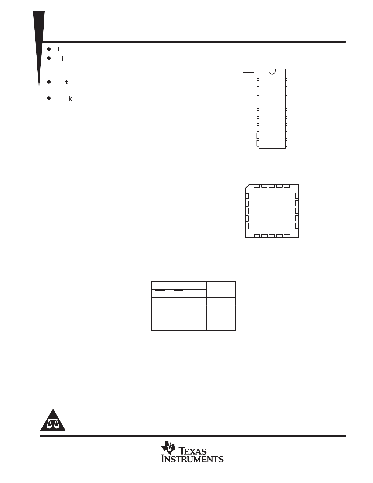
1
2
3
4
5
6
7
8
9
10
20
19
18
17
16
15
14
13
12
11
OE1
A1
A2
A3
A4
A5
A6
A7
A8
GND
V
CC
OE2
Y1
Y2
Y3
Y4
Y5
Y6
Y7
Y8
SN54HCT541 ...J OR W PACKAGE
SN74HCT541 . . . DW OR N PACKAGE
(TOP VIEW)
3212019
910111213
4
5
6
7
8
18
17
16
15
14
Y1
Y2
Y3
Y4
Y5
A3
A4
A5
A6
A7
A2
A1
OE1
Y7
Y6
V
OE2
A8
GND
Y8
SN54HCT541 . . . FK PACKAGE
(TOP VIEW)
CC
Copyright 1997, Texas Instruments Incorporated
PRODUCTION DATA information is current as of publication date.
Products conform to specifications per the terms of Texas Instruments
standard warranty. Production processing does not necessarily include
testing of all parameters.

SN54HCT541, SN74HCT541
OCTAL BUFFERS AND LINE DRIVERS
WITH 3-STATE OUTPUTS
SCLS306A – JANUARY 1996 – REVISED MA Y 1997
2
POST OFFICE BOX 655303 • DALLAS, TEXAS 75265
logic symbol
†
2
A1
3
A2
4
A3
1
Y1
18
Y2
17
Y3
16
&
EN
5
A4
6
A5
7
A6
Y4
15
Y5
14
Y6
13
19
OE1
OE2
8
A7
9
A8
Y7
12
Y8
11
†
This symbol is in accordance with ANSI/IEEE Std 91-1984 and IEC Publication 617-12.
logic diagram (positive logic)
OE1
OE2
To Seven Other Channels
A1
Y1
1
19
218
absolute maximum ratings over operating free-air temperature range
‡
Supply voltage range, V
CC
–0.5 V to 7 V. . . . . . . . . . . . . . . . . . . . . . . . . . . . . . . . . . . . . . . . . . . . . . . . . . . . . . . . . .
Input clamp current, I
IK
(V
I
< 0 or V
I
> V
CC
) (see Note 1) ±20 mA. . . . . . . . . . . . . . . . . . . . . . . . . . . . . . . . . . . .
Output clamp current, I
OK
(V
O
< 0 or V
O
> V
CC
) (see Note 1) ±20 mA. . . . . . . . . . . . . . . . . . . . . . . . . . . . . . . .
Continuous output current, I
O
(V
O
= 0 to V
CC
) ±35 mA. . . . . . . . . . . . . . . . . . . . . . . . . . . . . . . . . . . . . . . . . . . . . .
Continuous current through V
CC
or GND ±70 mA. . . . . . . . . . . . . . . . . . . . . . . . . . . . . . . . . . . . . . . . . . . . . . . . . . .
Package thermal impedance, θ
JA
(see Note 2): DW package 97°C/W. . . . . . . . . . . . . . . . . . . . . . . . . . . . . . . . .
N package 67°C/W. . . . . . . . . . . . . . . . . . . . . . . . . . . . . . . . . . .
Storage temperature range, T
stg
–65°C to 150°C. . . . . . . . . . . . . . . . . . . . . . . . . . . . . . . . . . . . . . . . . . . . . . . . . . .
‡
Stresses beyond those listed under “absolute maximum ratings” may cause permanent damage to the device. These are stress ratings only, and
functional operation of the device at these or any other conditions beyond those indicated under “recommended operating conditions” is not
implied. Exposure to absolute-maximum-rated conditions for extended periods may affect device reliability.
NOTES: 1. The input and output voltage ratings may be exceeded if the input and output current ratings are observed.
2. The package thermal impedance is calculated in accordance with JESD 51, except for through-hole packages, which use a trace
length of zero.
 Loading...