


 Loading...
Texas Instruments LV70036DSER, TLV70012DCKR, TLV70012DDCR, TLV70012DSER, TLV70013DDCR Schematic [ru]
...PRODUCT |
SAMPLE & |
TECHNICAL |
TOOLS & |
SUPPORT & |
FOLDER |
BUY |
DOCUMENTS |
SOFTWARE |
COMMUNITY |
TLV700
SLVSA00E –SEPTEMBER 2009–REVISED APRIL 2015
TLV700 200-mA, Low-IQ, Low-Dropout Regulator for Portable Devices
1 Features
•Very Low Dropout:
–43 mV at IOUT = 50 mA, VOUT = 2.8 V
–85 mV at IOUT = 100 mA, VOUT = 2.8 V
–175 mV at IOUT = 200 mA, VOUT = 2.35 V
•2% Accuracy
•Low IQ: 31 μA
•Available in Fixed-Output Voltages from 1.2 V to 4.8 V
•High PSRR: 68 dB at 1 kHz
•Stable With Effective Capacitance of 0.1 μF(1)
•Thermal Shutdown and Overcurrent Protection
•Available in 1.5-mm × 1.5-mm SON-6, SOT23-5, and SC-70 Packages
(1)See the Input and Output Capacitor Requirements.
2 Applications
•Wireless Handsets
•Smart Phones, PDAs
•ZigBee® Networks
•Bluetooth® Devices
•Li-Ion Operated Handheld Products
•WLAN and Other PC Add-on Cards
3 Description
The TLV700 series of low-dropout (LDO) linear regulators are low quiescent current devices with excellent line and load transient performance. These LDOs are designed for power-sensitive applications. A precision bandgap and error amplifier provides overall 2% accuracy. Low output noise, very high power-supply rejection ratio (PSRR), and low dropout voltage make this series of devices ideal for most battery-operated handheld equipment. All device versions have thermal shutdown and current limit for safety.
Furthermore, these devices are stable with an effective output capacitance of only 0.1 μF. This feature enables the use of cost-effective capacitors that have higher bias voltages and temperature derating. The devices regulate to specified accuracy with no output load.
The TLV700 series of LDOs are available in 1.5-mm × 1.5-mm SON-6, SOT-5, and SC70 packages.
Device Information(1)
PART NUMBER |
PACKAGE |
BODY SIZE (NOM) |
|
SC70 (5) |
2.00 mm × 1.25 mm |
TL700xx |
SOT (5) |
2.90 mm × 1.60 mm |
|
WSON (6) |
1.50 mm × 1.50 mm |
(1)For all available packages, see the orderable addendum at the end of the data sheet.
Typical Application Circuit
VIN |
|
IN |
OUT |
|
VOUT |
|
CIN |
|
|
COUT |
1 F |
|
|
|
CERAMIC |
||
|
|
|
TLV700XX |
|
|
|
|
ON |
|
|
|
|
OFF |
EN |
|
|
|
|
|
|
|
|
|
|
|
|
GND |
|
|
An IMPORTANT NOTICE at the end of this data sheet addresses availability, warranty, changes, use in safety-critical applications, intellectual property matters and other important disclaimers. PRODUCTION DATA.
TLV700
SLVSA00E –SEPTEMBER 2009–REVISED APRIL 2015 www.ti.com
Table of Contents
1 |
Features .................................................................. |
1 |
8 |
Application and Implementation ........................ |
13 |
||
2 |
Applications ........................................................... |
1 |
|
8.1 |
Application Information............................................ |
13 |
|
3 |
Description ............................................................. |
1 |
|
8.2 |
Typical Application .................................................. |
13 |
|
4 |
Revision History..................................................... |
2 |
9 |
Power Supply Recommendations...................... |
14 |
||
5 |
Pin Configuration and Functions ......................... |
4 |
10 |
Layout................................................................... |
15 |
||
6 |
Specifications......................................................... |
5 |
|
10.1 |
Layout Guidelines ................................................. |
15 |
|
|
6.1 |
Absolute Maximum Ratings |
5 |
|
10.2 |
Layout Examples................................................... |
15 |
|
|
10.3 |
Thermal Protection |
15 |
|||
|
6.2 |
ESD Ratings |
5 |
|
|||
|
|
10.4 |
Power Dissipation |
16 |
|||
|
6.3 |
Recommended Operating Conditions |
5 |
|
|||
|
11 Device and Documentation Support |
17 |
|||||
|
6.4 |
Thermal Information .................................................. |
5 |
||||
|
6.5 |
Electrical Characteristics........................................... |
6 |
|
11.1 |
Device Support .................................................... |
17 |
|
6.6 |
Typical Characteristics .............................................. |
7 |
|
11.2 |
Documentation Support ........................................ |
17 |
7 |
Detailed Description ............................................ |
11 |
|
11.3 |
Trademarks ........................................................... |
17 |
|
|
7.1 |
Overview |
11 |
|
11.4 |
Electrostatic Discharge Caution............................ |
17 |
|
|
11.5 |
Glossary |
17 |
|||
|
7.2 |
Functional Block Diagram |
11 |
|
|||
|
12 Mechanical, Packaging, and Orderable |
|
|||||
|
7.3 |
Feature Description................................................. |
11 |
|
|||
|
7.4 |
Device Functional Modes........................................ |
12 |
|
Information ........................................................... |
18 |
|
|
|
|
|
|
|
|
|
4 Revision History
NOTE: Page numbers for previous revisions may differ from page numbers in the current version.
Changes from Revision D (October 2012) to Revision E |
Page |
•Added ESD Ratings table, Feature Description section, Device Functional Modes, Application and Implementation section, Power Supply Recommendations section, Layout section, Device and Documentation Support section, and
|
Mechanical, Packaging, and Orderable Information section ................................................................................................. |
|
1 |
• Deleted Applications bullet for MP3 Players .......................................................................................................................... |
|
1 |
|
• |
Changed front-page graphic .................................................................................................................................................. |
|
1 |
• Changed Pin Configuration and Functions section; updated table format ............................................................................ |
|
4 |
|
• Changed "free-air temperature" to "junction temperature" in Absolute Maximum Ratings condition statement |
.................... 5 |
||
• Deleted Dissipation Ratings table .......................................................................................................................................... |
|
5 |
|
• Changed Thermal Information table; updated thermal resistance values for all packages ................................................... |
5 |
||
Changes from Revision C (July 2011) to Revision D |
|
Page |
|
• |
Updated Figure 5.................................................................................................................................................................... |
|
7 |
Changes from Revision B (December, 2010) to Revision C |
|
Page |
|
• Added footnote 2 to Absolute Maximum Ratings table .......................................................................................................... |
|
5 |
|
• Changed output current limit typical and maximum specifications......................................................................................... |
|
6 |
|
• Deleted previous Figure 12, Current Limit vs Input Voltage typical characteristic ................................................................. |
7 |
||
Changes from Revision A (April, 2010) to Revision B |
|
Page |
|
• Removed TLV701xx device references throughout document .............................................................................................. |
|
1 |
|
• Changed minimum output voltage available from 0.7 V to 1.2 V ........................................................................................... |
|
1 |
|
• |
Added footnote (1).................................................................................................................................................................. |
|
1 |
• Deleted VOUT < 1 V specification ............................................................................................................................................ |
|
6 |
|
• Deleted Active pulldown resistance parameter ...................................................................................................................... |
|
6 |
|
2 |
Submit Documentation Feedback |
Copyright © 2009–2015, Texas Instruments Incorporated |
|
|
Product Folder Links: TLV700 |
|
|

|
|
TLV700 |
www.ti.com |
SLVSA00E –SEPTEMBER 2009–REVISED APRIL 2015 |
|
• Changed Figure 4 title ............................................................................................................................................................ |
|
7 |
• Changed Figure 5 title ............................................................................................................................................................ |
|
7 |
• Removed TLV701xx block diagram...................................................................................................................................... |
|
11 |
• Revised Shutdown section ................................................................................................................................................... |
|
11 |
• Updated Application Information section to reflect minimum output voltage availability of 1.2 V |
........................................ 13 |
|
• Deleted references to TLV701xx throughout Application Information .................................................................................. |
|
13 |
• Changed footnote 2 for Ordering Information table to reflect minimum output voltage of 1.2 V ......................................... |
17 |
|
Copyright © 2009–2015, Texas Instruments Incorporated |
Submit Documentation Feedback |
3 |
Product Folder Links: TLV700

TLV700
SLVSA00E –SEPTEMBER 2009–REVISED APRIL 2015 |
|
|
|
|
|
www.ti.com |
||||
5 Pin Configuration and Functions |
|
|
|
|
|
|
||||
|
DSE Package |
|
|
DCK Package |
|
|||||
|
6-Pin WSON |
|
|
|
||||||
|
|
Top View |
|
|
5-Pin SC70 |
|
||||
|
|
|
|
|
Top View |
|
||||
|
|
|
|
|
|
|
|
|||
IN |
1 |
6 |
|
EN |
|
|
|
|
|
|
|
|
|
|
|
|
|
||||
GND |
2 |
5 |
|
N/C(1) |
IN |
|
1 |
5 |
|
OUT |
|
|
|
||||||||
OUT |
3 |
4 |
|
N/C(1) |
GND |
|
2 |
|
|
|
|
|
|
|
|
||||||
|
|
|
|
|
EN |
|
3 |
4 |
|
N/C(1) |
|
|
|
|
|
|
|
||||
|
|
|
|
|
|
|
|
|
|
|
DDC Package
5-Pin SOT
Top View
|
|
|
|
|
|
|
IN |
|
1 |
5 |
|
OUT |
|
|
|
|
|
|
|
|
|
||||
|
|
|
|
|
|
GND |
|
2 |
|
|
|
|
|
|
|
|
|
|
|
|
|
|
|||
|
|
|
|
|
|
EN |
|
3 |
4 |
|
N/C(1) |
|
|
|
|
|
|
|
|
|
|||||
(1) |
No connection. |
|
|
|
|
|
|
|
|
|
||
|
|
|
|
|
|
|
|
|
||||
|
|
|
|
|
|
|
|
Pin Functions |
|
|||
|
|
PIN |
|
I/O |
|
|
|
|
|
|
DESCRIPTION |
|
NAME |
WSON |
|
SC70 |
SOT |
|
|
|
|
|
|
||
|
|
|
|
|
|
|
|
|
||||
|
|
|
|
|
|
|
Input pin. A small, 1-μF ceramic capacitor is recommended from this pin to ground |
|||||
IN |
1 |
|
1 |
1 |
I |
|
to assure stability and good transient performance. See Input and Output |
|||||
|
|
|
|
|
|
|
Capacitor Requirements for more details. |
|||||
GND |
2 |
|
2 |
2 |
— |
|
Ground pin |
|
|
|
||
|
|
|
|
|
|
|
Enable pin. Driving EN over 0.9 V turns on the regulator. Driving EN below 0.4 V |
|||||
EN |
6 |
|
3 |
3 |
I |
|
puts the regulator into shutdown mode and reduces operating current to 1 μA, |
|||||
|
|
|
|
|
|
|
nominal. |
|
|
|
||
NC |
4, 5 |
|
4 |
4 |
— |
|
No connection. This pin can be tied to ground to improve thermal dissipation. |
|||||
|
|
|
|
|
|
|
Regulated output voltage pin. A small, 1-μF ceramic capacitor is needed from this |
|||||
OUT |
3 |
|
5 |
5 |
O |
|
pin to ground to assure stability. See Input and Output Capacitor Requirements for |
|||||
|
|
|
|
|
|
|
more details. |
|
|
|
||
4 |
Submit Documentation Feedback |
Copyright © 2009–2015, Texas Instruments Incorporated |
Product Folder Links: TLV700

|
|
|
|
|
|
TLV700 |
|
www.ti.com |
|
SLVSA00E –SEPTEMBER 2009–REVISED APRIL 2015 |
|||||
6 |
Specifications |
|
|
|
|
||
6.1 |
Absolute Maximum Ratings |
|
|
|
|
||
over operating junction temperature range (unless otherwise noted) (1) |
|
|
|
|
|||
|
|
|
MIN |
|
MAX |
UNIT |
|
|
|
VIN |
–0.3 |
6 |
|
||
Voltage |
V |
–0.3 |
6(2) |
V |
|||
|
|
EN |
|
|
|
|
|
|
|
VOUT |
–0.3 |
6 |
|
||
Maximum output current |
IOUT |
Internally limited |
|
||||
Output short-circuit duration |
|
Indefinite |
|
||||
Temperature |
Operating junction, TJ |
–55 |
150 |
°C |
|||
Storage, Tstg |
–55 |
150 |
|||||
|
|
|
|||||
(1)Stresses beyond those listed under Absolute Maximum Ratings may cause permanent damage to the device. These are stress ratings only, which do not imply functional operation of the device at these or any other conditions beyond those indicated under Recommended Operating Conditions. Exposure to absolute-maximum-rated conditions for extended periods may affect device reliability.
(2)VEN absolute maximum rating is VIN + 0.3 V or 6 V, whichever is less.
6.2 |
ESD Ratings |
|
|
|
|
|
|
VALUE |
UNIT |
|
|
Human body model (HBM), per ANSI/ESDA/JEDEC JS-001, all pins(1) |
±2000 |
|
V(ESD) |
Electrostatic discharge |
Charged device model (CDM), per JEDEC specification JESD22-C101, |
±500 |
V |
|
|
all pins(2) |
|
(1)JEDEC document JEP155 states that 500-V HBM allows safe manufacturing with a standard ESD control process.
(2)JEDEC document JEP157 states that 250-V CDM allows safe manufacturing with a standard ESD control process.
6.3 |
Recommended Operating Conditions |
|
|
|
|
over operating free-air temperature range (unless otherwise noted) |
|
|
|
||
|
|
MIN |
NOM |
MAX |
UNIT |
VIN |
|
2 |
|
5.5 |
V |
VOUT |
|
1.2 |
|
4.8 |
V |
IOUT |
|
0 |
|
200 |
mA |
6.4 Thermal Information
|
|
|
TLV700 |
|
|
|
|
THERMAL METRIC(1) |
DCK [SC70] |
DDC [SOT] |
DSE [WSON] |
UNIT |
|
|
|
5 PINS |
5 PINS |
6 PINS |
|
|
RθJA |
Junction-to-ambient thermal resistance |
307.6 |
235.9 |
321.3 |
|
|
RθJC(top) |
Junction-to-case (top) thermal resistance |
79.1 |
61.9 |
207.9 |
|
|
RθJB |
Junction-to-board thermal resistance |
93.7 |
54 |
281.5 |
°C/W |
|
ψJT |
Junction-to-top characterization parameter |
1.3 |
0.8 |
42.4 |
||
|
||||||
ψJB |
Junction-to-board characterization parameter |
92.8 |
53.4 |
284.8 |
|
|
RθJC(bot) |
Junction-to-case (bottom) thermal resistance |
n/a |
n/a |
142.3 |
|
(1)For more information about traditional and new thermal metrics, see the IC Package Thermal Metrics application report, SPRA953.
Copyright © 2009–2015, Texas Instruments Incorporated |
Submit Documentation Feedback |
5 |
Product Folder Links: TLV700

TLV700
SLVSA00E –SEPTEMBER 2009–REVISED APRIL 2015 |
www.ti.com |
6.5 Electrical Characteristics
At VIN = VOUT(nom) + 0.3 V or 2 V (whichever is greater); IOUT = 10 mA, VEN = 0.9 V, COUT = 1 μF, and TJ = –40°C to +125°C, unless otherwise noted. Typical values are at TJ = 25°C.
|
|
PARAMETER |
TEST CONDITIONS |
MIN |
TYP |
MAX |
UNIT |
|
VIN |
|
Input voltage range |
|
|
2 |
|
5.5 |
V |
VOUT |
|
DC output accuracy |
–40°C ≤ TJ ≤ +125°C |
–2% |
|
2% |
|
|
VOUT( |
VIN) |
Line regulation |
VOUT(nom) + 0.3 V ≤ VIN ≤ 5.5 V, |
|
1 |
5 |
mV |
|
IOUT = 10 mA |
|
|
||||||
|
|
|
|
|
|
|
|
|
VOUT( |
IOUT) |
Load regulation |
0 mA ≤ IOUT ≤ 200 mA |
|
1 |
15 |
mV |
|
|
|
|
VIN = 0.98 × VOUT(nom), IOUT = 50 mA, |
|
43 |
|
|
|
|
|
|
VOUT = 2.8 V |
|
|
|
|
|
V |
|
Dropout voltage(1) |
VIN = 0.98 × VOUT(nom), IOUT = 100 mA, |
|
85 |
|
mV |
|
DO |
|
|
VOUT = 2.8 V |
|
|
|
|
|
|
|
|
|
|
|
|
|
|
|
|
|
VIN = 0.98 × VOUT(nom), IOUT = 200 mA, |
|
175 |
250 |
|
|
|
|
|
VOUT = 2.35 V |
|
|
|
|
|
ICL |
|
Output current limit |
VOUT = 0.9 × VOUT(nom) |
220 |
|
860 |
mA |
|
IGND |
|
Ground pin current |
IOUT = 0 mA |
|
|
31 |
55 |
μA |
|
IOUT = 200 mA, VIN = VOUT + 0.5 V |
|
270 |
|
||||
|
|
|
|
|
|
|||
ISHDN |
|
Ground pin current (shutdown) |
VEN ≤ 0.4 V, VIN = 2 V |
|
400 |
|
nA |
|
|
VEN ≤ 0.4 V, 2 V ≤ VIN ≤ 4.5 V |
|
1 |
2 |
μA |
|||
|
|
|
|
|||||
PSRR |
|
Power-supply rejection ratio |
VIN = 2.3 V, VOUT = 1.8 V, |
|
68 |
|
dB |
|
|
|
|
IOUT = 10 mA, f = 1 kHz |
|
|
|
|
|
Vn |
|
Output noise voltage |
BW = 100 Hz to 100 kHz, |
|
48 |
|
μVRMS |
|
|
VIN = 2.3 V, VOUT = 1.8 V, IOUT = 10 mA |
|
|
|||||
|
|
|
|
|
|
|
||
t |
|
Start-up time(2) |
C = 1 μF, I |
= 200 mA |
|
100 |
|
μs |
STR |
|
|
OUT |
OUT |
|
|
|
|
VEN(high) |
|
Enable pin high (enabled) |
|
|
0.9 |
|
VIN |
V |
VEN(low) |
|
Enable pin low (disabled) |
|
|
0 |
|
0.4 |
V |
IEN |
|
Enable pin current |
VIN = VEN = 5.5 V |
|
0.04 |
0.5 |
μA |
|
UVLO |
|
Undervoltage lockout |
VIN rising |
|
|
1.9 |
|
V |
Tsd |
|
Thermal shutdown temperature |
Shutdown, temperature increasing |
|
160 |
|
°C |
|
|
Reset, temperature decreasing |
|
140 |
|
||||
|
|
|
|
|
|
|||
TJ |
|
Operating junction temperature |
|
|
–40 |
|
125 |
°C |
(1)VDO is measured for devices with VOUT(nom) ≥ 2.35 V.
(2)Start-up time = time from EN assertion to 0.98 × VOUT(nom).
6 |
Submit Documentation Feedback |
Copyright © 2009–2015, Texas Instruments Incorporated |
Product Folder Links: TLV700
TLV700
www.ti.com |
SLVSA00E –SEPTEMBER 2009–REVISED APRIL 2015 |
6.6 Typical Characteristics
Over operating temperature range (TJ = –40°C to +125°C), VIN = VOUT(nom) + 0.5 V or 2 V, whichever is greater; IOUT = 10 mA, VEN = VIN, COUT = 1 μF, unless otherwise noted. Typical values are at TJ = 25°C.
|
1.90 |
|
|
|
|
|
|
|
|
|
|
|
|
|
|
|
|
|
|
|
|
1.88 |
|
IOUT = 10 MA |
|
|
|
|
|
|
|
|
|
|
|
|
|
|
|
||
|
|
|
|
|
|
|
|
|
|
|
|
|
|
|
|
|
|
|
|
|
(V) |
1.86 |
|
|
|
|
|
|
|
|
|
|
|
|
|
|
|
|
|
|
|
|
|
|
|
|
|
|
|
|
|
|
|
|
|
|
|
|
|
|
||
1.84 |
|
|
|
|
|
|
|
|
|
|
|
|
|
|
|
|
|
|
|
|
VOLTAGE |
1.82 |
|
|
|
|
|
|
|
|
|
|
|
|
|
|
|
|
|
|
|
|
|
|
|
|
|
|
|
|
|
|
|
|
|
|
|
|
|
|
|
|
OUTPUT |
1.80 |
|
|
|
|
|
|
|
|
|
|
|
|
|
|
|
|
|
|
|
|
|
|
|
|
|
|
|
|
|
|
|
|
|
|
|
|
|
|
||
|
|
|
|
|
|
|
|
|
|
|
|
|
|
|
|
|
|
|
||
1.76 |
|
|
|
|
|
|
|
|
|
|
|
|
|
|
|
|
|
|
|
|
|
1.78 |
|
|
|
|
|
|
|
|
|
|
|
|
|
|
|
|
|
|
|
|
|
|
|
|
|
|
|
|
|
|
|
|
|
|
|
+125°C |
|
|
||
|
|
|
|
|
|
|
|
|
|
|
|
|
|
|
|
|||||
|
|
|
|
|
|
|
|
|
|
|
|
|
|
|
|
|
|
|||
|
1.74 |
|
|
|
|
|
|
|
|
|
|
|
|
|
|
|
+85°C |
|
|
|
|
|
|
|
|
|
|
|
|
|
|
|
|
|
|
||||||
|
1.72 |
|
|
|
|
|
|
|
|
|
|
|
|
|
|
|
+25°C |
|
|
|
|
|
|
|
|
|
|
|
|
|
|
|
|
|
|
|
−40°C |
|
|
||
|
|
|
|
|
|
|
|
|
|
|
|
|
|
|
|
|
|
|
||
|
1.70 |
|
|
|
|
|
|
|
|
|
|
|
|
|
|
|
|
|
|
|
|
|
|
|
|
|
|
|
|
|
|
|
|
|
|
|
|
|
|
|
|
|
2.1 |
2.6 |
3.1 |
3.6 |
4.1 |
4.6 |
5.1 |
5.6 |
||||||||||||
INPUT VOLTAGE (V)
Figure 1. TLV70018 Line Regulation
|
1.90 |
|
|
|
|
|
|
|
|
|
|
|
|
|
|
|
|
|
|
|
|
|
|
|
|
1.88 |
|
|
|
|
|
|
|
|
|
|
|
|
|
|
|
|
|
|
|
|
|
|
|
|
|
|
|
|
|
|
|
|
|
|
|
|
|
|
|
|
|
|
|
|
|
|
|
|
(V) |
1.86 |
|
|
|
|
|
|
|
|
|
|
|
|
|
|
|
|
|
|
|
|
|
|
|
|
|
|
|
|
|
|
|
|
|
|
|
|
|
|
|
|
|
|
|
|
|
|
||
1.84 |
|
|
|
|
|
|
|
|
|
|
|
|
|
|
|
|
|
|
|
|
|
|
|
|
VOLTAGE |
|
|
|
|
|
|
|
|
|
|
|
|
|
|
|
|
|
|
|
|
|
|
|
|
1.82 |
|
|
|
|
|
|
|
|
|
|
|
|
|
|
|
|
|
|
|
|
|
|
|
|
|
|
|
|
|
|
|
|
|
|
|
|
|
|
|
|
|
|
|
|
|
|
|
|
|
OUTPUT |
1.80 |
|
|
|
|
|
|
|
|
|
|
|
|
|
|
|
|
|
|
|
|
|
|
|
|
|
|
|
|
|
|
|
|
|
|
|
|
|
|
|
|
|
|
|
|
|
|
||
1.76 |
|
|
|
|
|
|
|
|
|
|
|
|
|
|
|
|
|
|
|
|
|
|
|
|
|
1.78 |
|
|
|
|
|
|
|
|
|
|
|
|
|
|
|
|
|
|
|
|
|
|
|
|
|
|
|
|
|
|
|
|
|
|
|
|
|
|
|
|
|
|
|
+125°C |
|
|
||
|
|
|
|
|
|
|
|
|
|
|
|
|
|
|
|
|
|
|
|
|
||||
|
|
|
|
|
|
|
|
|
|
|
|
|
|
|
|
|
|
|
|
|
|
|||
|
1.74 |
|
|
|
|
|
|
|
|
|
|
|
|
|
|
|
|
|
|
+85°C |
|
|
||
|
|
|
|
|
|
|
|
|
|
|
|
|
|
|
|
|
|
|
|
|||||
|
1.72 |
|
|
|
|
|
|
|
|
|
|
|
|
|
|
|
|
|
|
+25°C |
|
|
||
|
|
|
|
|
|
|
|
|
|
|
|
|
|
|
|
|
|
|
−40°C |
|
|
|||
|
|
|
|
|
|
|
|
|
|
|
|
|
|
|
|
|
|
|
|
|
|
|||
|
1.70 |
|
|
|
|
|
|
|
|
|
|
|
|
|
|
|
|
|
|
|
|
|
|
|
|
|
|
|
|
|
|
|
|
|
|
|
|
|
|
|
|
|
|
|
|
|
|
|
|
|
0 |
20 |
40 |
60 |
80 |
100 |
120 |
140 |
160 |
180 |
200 |
|||||||||||||
OUTPUT CURRENT(MA)
Figure 3. TLV70018 Load Regulation
|
180 |
|
|
|
|
|
|
|
|
160 |
|
|
|
|
|
|
|
(MV) |
140 |
|
|
|
|
|
|
|
120 |
|
|
|
|
|
|
|
|
VOLTAGE |
100 |
|
|
|
|
|
|
|
80 |
|
|
|
|
|
|
|
|
ROPOUT |
|
|
|
|
|
|
|
|
60 |
|
|
|
|
|
|
|
|
|
|
|
|
|
|
+125°C |
||
D |
|
|
|
|
|
|
||
40 |
|
|
|
|
|
|
|
|
|
|
|
|
|
|
+85°C |
||
|
|
|
|
|
|
|
||
|
20 |
|
|
|
|
|
+25°C |
|
|
|
|
|
|
|
-40°C |
||
|
|
|
|
|
|
|
||
|
0 |
|
|
|
|
|
|
|
|
0 |
30 |
60 |
90 |
120 |
150 |
180 |
210 |
|
|
|
|
OUTPUT CURRENT (MA) |
|
|
|
|
|
1.90 |
|
|
|
|
|
|
|
|
|
|
|
|
|
|
|
|
|
|
|
|
|
|
IOUT = 200 MA |
|
|
|
|
|
|
|
|
|
|
|
|
|
|
|
||
|
1.88 |
|
|
|
|
|
|
|
|
|
|
|
|
|
|
|
|
|
|
|
(V) |
1.86 |
|
|
|
|
|
|
|
|
|
|
|
|
|
|
|
|
|
|
|
|
|
|
|
|
|
|
|
|
|
|
|
|
|
|
|
|
|
|
||
1.84 |
|
|
|
|
|
|
|
|
|
|
|
|
|
|
|
|
|
|
|
|
VOLTAGE |
1.82 |
|
|
|
|
|
|
|
|
|
|
|
|
|
|
|
|
|
|
|
|
|
|
|
|
|
|
|
|
|
|
|
|
|
|
|
|
|
|
|
|
OUTPUT |
1.80 |
|
|
|
|
|
|
|
|
|
|
|
|
|
|
|
|
|
|
|
1.76 |
|
|
|
|
|
|
|
|
|
|
|
|
|
|
|
|
|
|
|
|
|
1.78 |
|
|
|
|
|
|
|
|
|
|
|
|
|
|
|
|
|
|
|
|
|
|
|
|
|
|
|
|
|
|
|
|
|
|
|
+125°C |
|
|
||
|
|
|
|
|
|
|
|
|
|
|
|
|
|
|
|
|||||
|
|
|
|
|
|
|
|
|
|
|
|
|
|
|
|
|
|
|||
|
1.74 |
|
|
|
|
|
|
|
|
|
|
|
|
|
|
|
+85°C |
|
|
|
|
|
|
|
|
|
|
|
|
|
|
|
|
|
|
||||||
|
1.72 |
|
|
|
|
|
|
|
|
|
|
|
|
|
|
|
+25°C |
|
|
|
|
|
|
|
|
|
|
|
|
|
|
|
|
|
|
|
−40°C |
|
|
||
|
|
|
|
|
|
|
|
|
|
|
|
|
|
|
|
|
|
|
||
|
1.70 |
|
|
|
|
|
|
|
|
|
|
|
|
|
|
|
|
|
|
|
|
|
|
|
|
|
|
|
|
|
|
|
|
|
|
|
|
|
|
|
|
|
2.1 |
2.6 |
3.1 |
3.6 |
4.1 |
4.6 |
5.1 |
5.6 |
||||||||||||
INPUT VOLTAGE (V)
|
|
Figure 2. TLV70018 Line Regulation |
||||
|
250 |
|
|
|
|
|
|
IOUT = 200 MA |
|
|
|
|
|
|
200 |
|
|
|
|
|
(MV) |
|
|
|
|
|
|
VOLTAGE |
150 |
|
|
|
|
|
ROPOUT |
100 |
|
|
|
|
|
D |
|
|
|
|
|
+125°C |
|
|
|
|
|
|
|
|
50 |
|
|
|
|
+85°C |
|
|
|
|
|
|
+25°C |
|
|
|
|
|
|
−40°C |
|
0 |
|
|
|
|
|
|
2.25 |
2.75 |
3.25 |
3.75 |
4.25 |
4.75 |
|
|
|
INPUT VOLTAGE (V) |
|
|
|
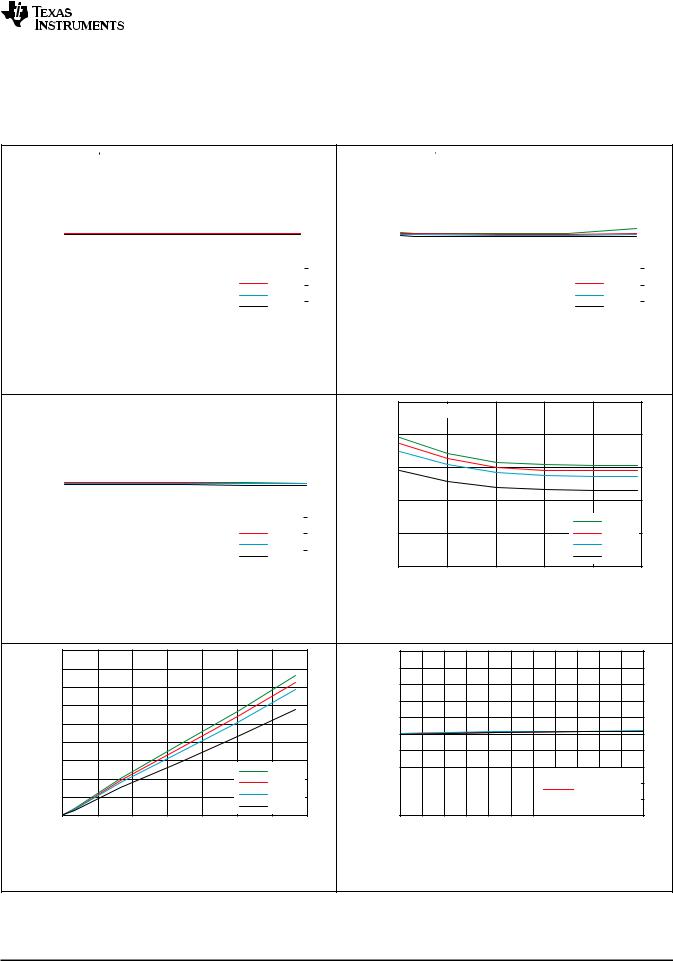
Figure 4. Dropout Voltage vs Input Voltage
|
1.90 |
|
1.88 |
(V) |
1.86 |
1.84 |
|
OLTAGEV |
1.82 |
OUTPUT |
1.80 |
1.76 |
|
|
1.78 |
1.74 
 IOUT = 200 MA IOUT = 10 MA 1.72
 IOUT = 150 MA
1.70 


 −40 −25 −10 5 20 35 50 65 80 95 110 125
TEMPERATURE (°C)
Figure 5. Dropout Voltage vs Output Current, VOUT = 4.8 V |
Figure 6. TLV70018 Output Voltage vs Temperature |
Copyright © 2009–2015, Texas Instruments Incorporated |
Submit Documentation Feedback |
7 |
Product Folder Links: TLV700

TLV700
SLVSA00E –SEPTEMBER 2009–REVISED APRIL 2015 |
www.ti.com |
Typical Characteristics (continued)
Over operating temperature range (TJ = –40°C to +125°C), VIN = VOUT(nom) + 0.5 V or 2 V, whichever is greater; IOUT = 10 mA, VEN = VIN, COUT = 1 μF, unless otherwise noted. Typical values are at TJ = 25°C.
|
50 |
|
|
|
|
|
|
|
300 |
|
|
|
|
|
|
|
|
|
|
|
IOUT = 0 MA |
|
|
|
|
|
|
|
|
|
|
|
|
|
|
|
|
|
|
|
45 |
|
|
|
|
|
|
|
|
|
|
|
|
|
|
|
|
|
|
|
40 |
|
|
|
|
|
|
|
250 |
|
|
|
|
|
|
|
|
|
|
(CPGURRENTINROUNDA) |
|
|
|
|
|
|
|
(CPGURRENTINROUNDA) |
|
|
|
|
|
|
|
|
|
|
|
35 |
|
|
|
|
|
|
|
|
|
|
|
|
|
|
|
|
|
||
|
|
|
|
|
|
|
|
|
200 |
|
|
|
|
|
|
|
|
|
|
|
30 |
|
|
|
|
|
|
|
|
|
|
|
|
|
|
|
|
|
|
|
25 |
|
|
|
|
|
|
|
150 |
|
|
|
|
|
|
|
|
|
|
|
20 |
|
|
|
|
|
|
|
|
|
|
|
|
|
|
|
|
|
|
|
15 |
|
|
|
|
|
|
|
100 |
|
|
|
|
|
|
|
|
|
|
|
|
|
|
|
|
+125°C |
|
|
|
|
|
|
|
|
|
+125°C |
|||
|
|
|
|
|
|
|
|
|
|
|
|
|
|
|
|
||||
|
10 |
|
|
|
|
|
+85°C |
50 |
|
|
|
|
|
|
|
|
+85°C |
||
|
|
|
|
|
|
|
+25°C |
|
|
|
|
|
|
|
|
+25°C |
|||
|
5 |
|
|
|
|
|
|
|
|
|
|
|
|
|
|
||||
|
|
|
|
|
|
−40°C |
|
|
|
|
|
|
|
|
|
−40°C |
|||
|
|
|
|
|
|
|
|
|
|
|
|
|
|
|
|
||||
|
0 |
|
|
|
|
|
|
|
0 |
|
|
|
|
|
|
|
|
|
|
|
2.1 |
2.6 |
3.1 |
3.6 |
4.1 |
4.6 |
5.1 |
5.6 |
0 |
20 |
40 |
60 |
80 |
100 |
120 |
140 |
160 |
180 |
200 |
|
|
|
|
INPUT VOLTAGE (V) |
|
|
|
|
|
|
|
OUTPUT CURRENT(MA) |
|
|
|
||||
Figure 7. TLV70018 Ground Pin Current vs Input Voltage |
Figure 8. TLV70018 Ground Pin Current vs Load |
|
40 |
|
|
|
|
|
2.0 |
|
|
|
|
|
|
|
|
35 |
|
|
|
|
|
1.8 |
|
|
|
|
|
|
|
|
|
|
|
|
|
|
|
|
|
|
|
|
|
|
GROUNDPINCURRENT( A) |
|
|
|
|
|
SHUTDOWNCURRENT( A) |
1.6 |
|
|
|
|
|
|
|
30 |
|
|
|
|
1.4 |
|
|
|
|
|
|
|
||
|
|
|
|
|
|
|
|
|
|
|
|
|||
25 |
|
|
|
|
1.2 |
|
|
|
|
|
|
|
||
|
|
|
|
|
|
|
|
|
|
|
|
|||
20 |
|
|
|
|
1.0 |
|
|
|
|
|
|
|
||
15 |
|
|
|
|
0.8 |
|
|
|
|
|
|
|
||
|
|
|
|
|
|
|
|
|
|
|
|
|||
|
|
|
|
|
0.6 |
|
|
|
|
|
|
|
||
10 |
|
|
|
|
0.4 |
|
|
|
|
|
+125°C |
|||
|
|
|
|
|
|
|
|
|
|
|||||
|
|
|
|
|
|
|
|
|
|
|
|
|||
|
5 |
|
|
|
|
|
0.2 |
|
|
|
|
|
+85°C |
|
|
|
|
|
|
|
|
|
|
|
|
|
|
||
|
|
|
|
|
IOUT = 0 MA |
|
|
|
|
|
|
+25°C |
||
|
|
|
|
|
|
|
|
|
|
|
|
|||
|
0 |
|
|
|
|
|
0 |
|
|
|
|
|
|
|
|
−40 |
−25 |
−10 |
5 |
20 35 50 65 80 95 110 125 |
|
2.1 |
2.6 |
3.1 |
3.6 |
4.1 |
4.6 |
5.1 |
5.6 |
|
|
|
|
|
TEMPERATURE (°C) |
|
|
|
|
INPUT VOLTAGE (V) |
|
|
|
|
Figure 9. TLV70018 Ground Pin Current vs Temperature |
Figure 10. TLV70018 Shutdown Current vs Input Voltage |
|
100 |
|
|
|
|
|
|
|
80 |
|
|
|
|
|
|
|
|
90 |
|
IOUT = 10 MA |
|
|
|
|
70 |
1KHZ |
|
|
|
|
|
|
|
|
|
|
|
|
|
|
|
|
|
|
|
|
|
|
|
|
|
80 |
|
|
|
IOUT = 150 MA |
|
|
|
|
|
|
|
|
|
|
|
|
|
|
|
|
|
|
60 |
|
10 KHZ |
|
|
|
|
|
||
|
70 |
|
|
|
|
|
|
|
|
|
|
|
|
|
|
|
PSRR(DB) |
60 |
|
|
|
|
|
|
PSRR(DB) |
50 |
|
|
|
|
|
|
|
|
|
|
|
|
|
|
|
|
|
|
|
|
|
|||
|
|
|
|
|
|
|
|
100 KHZ |
|
|
|
|
|
|
||
50 |
|
|
|
|
|
|
40 |
|
|
|
|
|
|
|
||
40 |
|
|
|
|
|
|
30 |
|
|
|
|
|
|
|
||
|
|
|
|
|
|
|
|
|
|
|
|
|
|
|||
|
|
|
|
|
|
|
|
|
|
|
|
|
|
|
|
|
|
30 |
|
|
|
|
|
|
|
|
|
|
|
|
|
|
|
|
|
|
|
|
|
|
|
|
20 |
|
|
|
|
|
|
|
|
20 |
|
|
|
|
|
|
|
|
|
|
|
|
|
|
|
|
10 |
|
|
|
|
|
|
|
10 |
|
|
|
|
|
|
|
|
|
|
|
VIN − VOUT = 0.5 V |
|
|
|
|
|
|
|
|
|
|||
|
|
|
|
|
|
|
|
|
|
|
|
|
|
|||
|
0 |
|
|
|
|
|
|
|
0 |
|
|
|
|
|
|
|
|
10 |
100 |
1 K |
10 K |
100 K |
1 M |
10 M |
|
2.1 |
2.2 |
2.3 |
2.4 |
2.5 |
2.6 |
2.7 |
2.8 |
|
|
|
|
FREQUENCY (HZ) |
|
|
|
|
|
|
INPUT VOLTAGE (V) |
|
|
|
||
Figure 11. TLV70018 Power-Supply Ripple Rejection vs |
Figure 12. TLV70018 Power-Supply Ripple Rejection vs |
Frequency |
Input Voltage |
8 |
Submit Documentation Feedback |
Copyright © 2009–2015, Texas Instruments Incorporated |
Product Folder Links: TLV700

TLV700
www.ti.com |
SLVSA00E –SEPTEMBER 2009–REVISED APRIL 2015 |
Typical Characteristics (continued)
Over operating temperature range (TJ = –40°C to +125°C), VIN = VOUT(nom) + 0.5 V or 2 V, whichever is greater; IOUT = 10 mA, VEN = VIN, COUT = 1 μF, unless otherwise noted. Typical values are at TJ = 25°C.
V/√HZ) |
10 |
|
|
|
|
|
|
|
|
|
|
|
|
|
|
( |
1 |
|
|
|
|
|
|
DENSITY |
|
|
|
|
|
|
|
|
|
|
|
|
|
|
|
NOISE |
0.1 |
|
|
|
|
|
|
|
|
|
|
|
|
|
|
OUTPUTSPECTRAL |
0.01 |
|
|
|
|
|
|
IOUT = 10 MA |
|
|
|
|
|
||
CIN = COUT = 1 F |
|
|
|
|
|||
0 |
|
|
|
|
|
|
|
|
|
|
|
|
|
|
|
|
10 |
100 |
1 K |
10 K |
100 K |
1 M |
10 M |
FREQUENCY (HZ)
Figure 13. TLV70018 Output Spectral Noise Density vs Output Voltage
|
|
|
|
|
|
|
|
|
|
|
|
|
|
|
|
|
|
|
|
|
|
|
|
|
|
|
|
|
|
|
|
|
|
TR = TF = 1 S |
|
|
|
|
|
|
|
|
|
|
|
|
|
|
|
|
|
|
|
|
|
|
|||||||||
20MA/DIV |
|
|
|
|
|
|
|
|
10 MA |
|
|
|
|
|
|
|
|
|
|
|||||||||||||
|
|
|
|
|
|
|
|
|
|
|
|
|
|
|
|
|
|
0 |
MA |
|
|
|
|
|
||||||||
|
|
|
|
|
|
|
|
|
|
|
|
|
|
|
|
|
|
|
|
|
|
|
|
|
|
|
||||||
|
|
|
|
|
|
|
|
|
|
|
|
|
|
|
|
|
|
|
|
|
|
|
|
|
||||||||
|
|
|
|
|
|
|
|
|
|
|
|
|
|
|
|
|
|
|
|
|
|
|
|
|
|
|
|
|
|
|
|
|
|
|
IOUT |
|
|
|
|
|
|
|
|
|
|
|
|
|
|
|
|
|
|
|
|
|
|
|
|
|
|
||||
5MV/DIV |
|
|
|
|
|
|
|
|
|
|
|
|
|
|
|
|
|
|
|
|
|
|
|
|
|
|
|
|
|
|
|
|
|
|
|
|
|
|
|
|
|
|
|
|
|
|
|
|
|
|
|
|
|
|
|
|
|
|
|
|
|
|
|
|
|
|
|
VOUT |
|
|
|
|
|
|
|
|
|
|
|
|
|
|
|
|
|
|
|
|
|
|
|
|
|
|
||||
|
|
|
|
|
|
|
|
|
|
|
|
|
|
|
|
|
|
|
|
|
|
|
|
|
|
|
||||||
|
|
|
|
|
|
|
|
|
|
|
|
|
|
|
|
|
|
|
|
|
|
|
|
|
|
|
|
|
|
|
|
|
|
|
|
|
|
|
|
|
|
|
|
|
|
|
|
|
|
|
|
|
|
|
|
|
|
|
|
|
|
|
|
|
|
|
|
|
|
|
|
|
|
|
|
|
|
|
|
|
|
|
|
|
|
|
|
VIN = 2.3 V |
|
|
||||||||
|
|
|
|
|
|
|
|
|
|
|
|
|
|
|
|
|
|
|
|
|
|
|
|
|
|
|
|
|
|
|
|
|
|
|
|
|
|
|
|
|
|
|
|
|
10 S/DIV |
||||||||||||||||||||
|
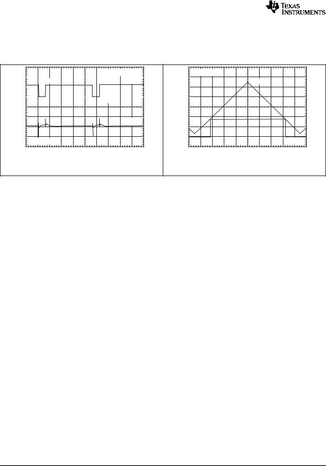
Figure 15. TLV70018 Load Transient Response |
|||||||||||||||||||||||||||||||
|
|
|
|
|
|
|
|
|
|
|
|
|
|
|
|
|
|
|
|
|
|
|
|
|
|
|
|
|
|
|
|
|
|
|
|
|
|
|
|
|
|
|
|
|
|
|
|
|
|
|
SLEW RATE = 1 V/ S |
|
|
||||||||||||
|
|
|
|
|
|
|
|
|
|
|
|
|
|
|
|
|
|
|
|
|
|
|
|
|
|
|
|
|
|
|
|
|
|
|
|
|
|
|
|
|
|
|
|
|
|
|
|
|
|
|
|
|
|
|
|
|
|
|
|
|
|
|
|
|
|
1V/DIV |
|
|
|
|
|
|
2.9 V |
|
|
|
|
|
|
|
|
|
|
|
|
|
|
|
|
VIN |
|
|
|
|
||||
|
|
|
|
|
|
|
|
|
|
|
|
|
|
|
|
|
|
|
|
|
|
|
|
|
|
|
|
|
|
|
|
|
|
|
|
|
|
|
|
|
|
|
|
|
|
|
2.3 V |
|
|
|
|
|
|
|
|
|
|
|
|
|
|||||
|
|
|
|
|
|
|
|
|
|
|
|
|
|
|
|
|
|
|
|
|
|
|
|
|
|
|
|
|||||
5MV/DIV |
|
|
|
|
|
|
|
|
|
|
|
|
|
|
|
|
|
|
|
|
|
|
|
|
|
|
|
|
|
|
|
|
|
|
|
|
|
|
|
|
|
|
|
|
|
|
|
|
|
|
|
|
|
|
|
|
|
|
|
|
|
|
|
|
|
|
|
|
|
|
|
|
|
|
|
|
|
|
|
|
|
|
|
|
|
|
|
|
|
VOUT |
|
|
|
|
||||
|
|
|
|
|
|
|
|
|
|
|
|
|
|
|
|
|
|
|
|
|
|
|
|
|
|
|
|
|
|
|
|
|
|
|
|
|
|
|
|
|
|
|
|
|
|
|
|
|
|
|
|
|
|
|
|
|
|
|
|
|
|
|
|
|
|
|
|
|
|
|
|
|
|
|
|
|
|
|
|
|
|
|
|
|
|
|
|
|
|
|
|
|
|
|
|
|
|
|
|
IOUT = 200 MA |
|
|
|
|
|
|
|
|
|
|
|
|
|
|
|
|
|
|
|
|
|
|
|
||||||||
|
|
|
|
|
|
|
|
|
|
|
|
|
|
|
|
|
|
|
|
|
|
|
|
|
|
|
|
|
|
|
|
|
|
|
|
|
|
|
|
|
|
|
|
|
|
|
|
|
|
|
|
|
|
|
TR = TF = 1 S |
|
|
|
|
|
200 MA |
|
|
|
|
|||||||||
100MA/DIV |
|
|
|
|
|
|
|
|
|
|
|
|
|
|
|
|
|
|
|
|
|
|
|
IOUT |
|
|
|
|
|
|
|
|
0 |
MA |
|
|
|||||
|
|
|
|
|
|
|
|
|
|
|
|
|
||||||||
50MV/DIV |
|
|
|
|
|
|
|
|
|
|
|
|
|
|
|
|
|
|
|
|
|
|
|
|
|
|
|
|
|
|
|
|
|
|
|
|
|
|
|
|
|
|
|
|
|
|
|
|
|
|
|
|
|
|
|
|
|
|
|
|
|
|
|
VOUT |
|
|
|
|
|
|
|
|
|
|
|
|
|
|
|
|
|||
|
|
|
|
|
|
|
|
|
|
|
|
|
|
|
|
|
|
|||
|
|
|
|
|
|
|
|
|
|
|
|
|
|
|
|
|
|
|
|
|
|
|
|
|
|
|
|
|
|
|
|
|
|
|
|
|
|
|
|
|
|
|
|
|
|
|
|
|
|
|
|
|
|
|
|
VIN = 2.1 V |
|
|||||
|
|
|
|
|
|
|
|
|
|
|
|
|
|
|
|
|
|
|
|
|
|
|
|
|
|
|
|
|
|
10 S/DIV |
|||||||||||
Figure 14. TLV70018 Load Transient Response
|
|
|
|
|
|
|
|
|
|
|
|
|
|
|
|
|
|
|
|
|
|
|
|
|
|
|
|
|
|
|
|
TR =TF = 1 S |
|
|
|
|
|
|
|
|
|
|
|
|
|
|
|
|
|
|
|
||||||||
|
|
|
|
|
|
|
|
|
|
|
|
|
|
|
|
|
|
|
|
|
|
|
|
||||||
A/DIV |
|
|
IOUT |
|
|
|
|
|
|
|
|
|
|
|
50 MA |
|
|
|
|
|
|||||||||
|
|
|
|
|
|
|
|
|
|
|
|
|
|
|
|
|
|
|
|
|
|
|
|
|
|
|
|
|
|
|
|
|
|
|
|
|
|
|
|
|
|
|
|
|
|
|
|
|
|
|
|
|
|
|
|
|
|
|
|
|
|
|
|
|
|
|
|
|
|
|
|
|
|
|
|
|
|
|
|
|
0 MA |
|
|
|
|
||||
50 M |
|
|
|
|
|
|
|
|
|
|
|
|
|
|
|
|
|
|
|
|
|
|
|
|
|||||
|
|
|
|
|
|
|
|
|
|
|
|
|
|
|
|
|
|
|
|
|
|
|
|
|
|
|
|
|
|
|
|
|
|
|
|
|
|
|
|
|
|
|
|
|
|
|
|
|
|
|
|
|
|
|
|
|
|
|
|
DIV |
|
|
|
|
|
|
|
|
|
|
|
|
|
|
|
|
|
|
|
|
|
|
|
|
|
|
|
||
|
|
|
|
|
|
|
|
|
|
|
|
|
|
|
|
|
|
|
|
|
|
|
|
|
|
|
|||
|
|
|
VOUT |
|
|
|
|
|
|
|
|
|
|
|
|
|
|
|
|
|
|
|
|
|
|||||
20 MV/ |
|
|
|
|
|
|
|
|
|
|
|
|
|
|
|
|
|
|
|
|
|
|
|
|
|
|
|
|
|
|
|
|
|
|
|
|
|
|
|
|
|
|
|
|
|
|
|
|
|
|
|
|
|
|
|
|
|
|
|
|
|
|
|
|
|
|
|
|
|
|
|
|
|
|
|
|
|
|
|
|
|
|
|
|
|
|
|
|
|
|
|
|
|
|
|
|
|
|
|
|
|
|
|
|
|
|
|
|
|
|
|
VIN = 2.3 V |
|
|
|||||
|
|
|
|
|
|
|
|
|
|
|
|
|
|
|
|
|
|
|
|
|
|
|
|
|
|
|
|
|
|
|
|
|
|
|
|
|
|
|
|
|
|
|
10 S/DIV |
||||||||||||||||
|
|
Figure 16. TLV70018 Load Transient Response |
|||||||||||||||||||||||||||
|
|
|
|
|
|
|
|
|
|
|
|
|
|
|
|
|
|
|
|
|
|
|
|
|
|
|
|
|
|
|
|
|
|
|
|
|
|
|
|
|
|
|
|
|
|
SLEW RATE = 1 V/ S |
|
|
|||||||||||
|
|
VIN |
|
|
|
|
|
||||||||||||||||||||||
1V/DIV |
|
|
|
|
2.7 V |
|
|
|
|
|
|
|
|
|
|
|
|
|
|
|
|
|
|
|
|||||
|
|
|
|
|
|
|
|
|
|
|
|
|
|
|
|
|
|
|
|
|
|
|
|
|
|
|
|
|
|
|
|
|
|
|
|
|
|
|
|
|
|
|
|
|
|
2.3 V |
|
|
|
|
|
|
|
|
|
||||
|
|
|
|
|
|
|
|
|
|
|
|
|
|
|
|
|
|
|
|
|
|
|
|
||||||
5MV/DIV |
|
|
|
|
|
|
|
|
|
|
|
|
|
|
|
|
|
|
|
|
|
|
|
|
|
|
|
|
|
|
|
|
|
|
|
|
|
|
|
|
|
|
|
|
|
|
|
|
|
|
|
|
|
|
|
|
|
|
|
|
|
|
|
|
|
|
|
|
|
|
|
|
|
|
|
|
|
|
|
|
VOUT |
|
||
|
|
|
|
|
|
|
|
|
|
|
|
|
|
|
|
|
|
|
IOUT = 1 MA |
|
|
|
|
|
|
|
|
|
|||||
|
|
|
|
|
|
|
|
|
|
|
|
|
|
|
|
|
1 MS/DIV |
1 MS/DIV |
Figure 17. TLV70018 Line Transient Response |
Figure 18. TLV70018 Line Transient Response |
Copyright © 2009–2015, Texas Instruments Incorporated |
Submit Documentation Feedback |
9 |
Product Folder Links: TLV700
TLV700
SLVSA00E –SEPTEMBER 2009–REVISED APRIL 2015 |
www.ti.com |
Typical Characteristics (continued)
Over operating temperature range (TJ = –40°C to +125°C), VIN = VOUT(nom) + 0.5 V or 2 V, whichever is greater; IOUT = 10 mA, VEN = VIN, COUT = 1 μF, unless otherwise noted. Typical values are at TJ = 25°C.
10MV/DIV 1V/DIV
SLEW RATE = 1 V/ S
|
5.5 V |
|
|
VIN |
|
||
|
|
|
|
|
|
|
|
|
|
|
|
|
|
|
|
2.1 V
VOUT
IOUT = 200 MA
IOUT = 1 MA |
VIN |
1V/DIV |
VOUT
1 MS/DIV |
200 MS/DIV |
Figure 19. TLV70018 Line Transient Response |
Figure 20. TLV70018 VIN Ramp-Up, Ramp-Down Response |
10 |
Submit Documentation Feedback |
Copyright © 2009–2015, Texas Instruments Incorporated |
Product Folder Links: TLV700
TLV700
www.ti.com |
SLVSA00E –SEPTEMBER 2009–REVISED APRIL 2015 |
7 Detailed Description
7.1 Overview
The TLV700 series of LDO linear regulators are low quiescent current devices with excellent line and load transient performance. These LDOs are designed for power-sensitive applications. A precision bandgap and error amplifier provides overall 2% accuracy. Low output noise, very high PSRR, and low dropout voltage make this series of devices ideal for most battery-operated handheld equipment. All device versions have integrated thermal shutdown, current limit, and undervoltage lockout (UVLO).
7.2 Functional Block Diagram
IN |
OUT |
|
Current |
|
Limit |
|
Thermal |
|
Shutdown |
|
UVLO |
EN |
Bandgap |
|
LOGIC |
|
TLV700XX SERIES |
|
GND |
7.3 Feature Description
7.3.1 Internal Current Limit
The TLV700 internal current limit helps to protect the regulator during fault conditions. During current limit, the output sources a fixed amount of current that is largely independent of the output voltage. In such a case, the
output voltage is not regulated, and is VOUT = ICL × RLOAD. The PMOS pass transistor dissipates (VIN – VOUT) × ICL until thermal shutdown is triggered and the device turns off. As the device cools down, it is turned on by the
internal thermal shutdown circuit. If the fault condition continues, the device cycles between current limit and thermal shutdown. See Thermal Protection for more details.
The PMOS pass element in the TLV700 has a built-in body diode that conducts current when the voltage at OUT exceeds the voltage at IN. This current is not limited, so if extended reverse voltage operation is anticipated, external limiting to 5% of the rated output current is recommended.
7.3.2 Shutdown
The enable pin (EN) is active high. The device is enabled when voltage at EN pin goes above 0.9 V. The device is turned off when the EN pin is held at less than 0.4 V. When shutdown capability is not required, EN can be connected to the IN pin.
Copyright © 2009–2015, Texas Instruments Incorporated |
Submit Documentation Feedback |
11 |
Product Folder Links: TLV700

TLV700
SLVSA00E –SEPTEMBER 2009–REVISED APRIL 2015 |
www.ti.com |
Feature Description (continued)
7.3.3 Dropout Voltage
The TLV700 uses a PMOS pass transistor to achieve low dropout. When (VIN – VOUT) is less than the dropout voltage (VDO), the PMOS pass device is in the linear region of operation and the input-to-output resistance is the
RDS(on) of the PMOS pass element. VDO scales approximately with output current because the PMOS device behaves as a resistor in dropout.
As with any linear regulator, PSRR and transient response are degraded as (VIN – VOUT) approaches dropout. This effect is shown in Figure 12 in Typical Characteristics.
7.3.4 Undervoltage Lockout (UVLO)
The TLV700 uses a UVLO circuit to keep the output shut off until internal circuitry is operating properly.
7.4 Device Functional Modes
7.4.1 Normal Operation
The device regulates to the nominal output voltage under the following conditions:
•The input voltage is greater than the nominal output voltage added to the dropout voltage.
•The output current is less than the current limit.
•The input voltage is greater than the UVLO voltage.
7.4.2 Dropout Operation
If the input voltage is lower than the nominal output voltage plus the specified dropout voltage, but all other conditions are met for normal operation, the device operates in dropout mode. In this condition, the output voltage is the same the input voltage minus the dropout voltage. The transient performance of the device is significantly degraded because the pass device is in a triode state and no longer regulates the output voltage of the LDO. Line or load transients in dropout may result in large output voltage deviations.
Table 1 lists the conditions that lead to the different modes of operation.
Table 1. Device Functional Mode Comparison
OPERATING MODE |
PARAMETER |
|
|
VIN |
IOUT |
||
|
|||
Normal mode |
VIN > VOUT(nom) + VDO |
IOUT < ICL |
|
Dropout mode |
VIN < VOUT(nom) + VDO |
IOUT < ICL |
|
Current limit |
VIN > UVLO |
IOUT > ICL |
12 |
Submit Documentation Feedback |
Copyright © 2009–2015, Texas Instruments Incorporated |
Product Folder Links: TLV700
Loading...