


Texas Instruments MSP430P112IDW, MSP430C112IDW, MSP-EVK430A110, MSP430C111IDW, MSP-EVK430X110 Datasheet
...MSP430x11x
MIXED SIGNAL MICROCONTROLLERS
SLAS196B± DECEMBER 1998 ± REVISED APRIL 2000
DLow Supply Voltage Range 2.5 V ± 5.5 V
DUltra Low-Power Consumption
DLow Operation Current, 330 A at 1 MHz,3 V
DTwo Power Saving Modes:
±Standby Mode: 1.5 A
±RAM Retention Off Mode: 0.1 A
DWake-up From Standby Mode in 6 s
Maximum
D16-Bit RISC Architecture, 200 ns Instruction Cycle Time
DBasic Clock Module Configurations:
±Various Internal Resistors
±Single External Resistor
±32 kHz Crystal
±High Frequency Crystal
±Resonator
±External Clock Source
DSingle Slope A/D Converter With External Components
D16-Bit Timer With 3 Capture/Compare Registers
DSerial Onboard Programming
DProgram Code Protection by Security Fuse
DFamily Members Include:
MSP430C111: 2k Byte ROM,128 Byte RAM MSP430C112: 4k Byte ROM, 256 Byte RAM MSP430P112: 4k Byte OTP, 256 Byte RAM
DEPROM Version Available for Prototyping:
±PMS430E112: 4k Byte EPROM, 256 Byte RAM
DAvailable in a 20-Pin Plastic Small-Outline Wide Body (SOWB) Package, 20-Pin Ceramic Dual-In-Line (CDIP) Package (EPROM Only)
description
The Texas Instruments MSP430 series is an ultra low-power microcontroller family consisting of several devices featuring different sets of modules targeted to various applications. The microcontroller is designed to be battery operated for an extended application lifetime. With 16-bit RISC architecture, 16 bit integrated registers on the CPU, and the constant generator, the MSP430 achieves maximum code efficiency. The digitallycontrolled oscillator provides fast wake-up from all low-power modes to active mode in less than 6 ms.
DW PACKAGE (TOP VIEW)
TEST/VPP |
|
|
1 |
20 |
|
|
P1.7/TA2/TDO/TDI |
||
|
|
|
|
||||||
|
|
|
|
||||||
|
VCC |
|
|
2 |
19 |
|
|
P1.6/TA1/TDI |
|
|
|
|
|
|
|||||
|
|
|
|
|
|||||
P2.5/ROSC |
|
3 |
18 |
|
|
P1.5/TA0/TMS |
|||
|
|
|
|
||||||
|
|
|
|||||||
|
|
VSS |
|
|
4 |
17 |
|
|
P1.4/SMCLK/TCK |
Xout/TCLK |
|
5 |
16 |
|
|
P1.3/TA2 |
|||
|
|
|
|
||||||
|
|
Xin |
|
|
6 |
15 |
|
|
P1.2/TA1 |
|
|
|
|
|
|
||||
|
|
|
|
|
|
|
|
|
P1.1/TA0 |
|
RST/NMI |
|
|
7 |
14 |
|
|
||
|
|
|
|
|
|||||
P2.0/ACLK |
|
|
8 |
13 |
|
|
P1.0/TACLK |
||
|
|
|
|
||||||
P2.1/INCLK |
|
|
9 |
12 |
|
|
P2.4/TA2 |
||
|
|
|
|
||||||
|
P2.2/TA0 |
|
|
10 |
11 |
|
|
P2.3/TA1 |
|
|
|
|
|
|
|||||
|
|
|
|
|
|
|
|
|
|
Typical applications include sensor systems that capture analog signals, convert them to digital values, and then process the data and display them or transmit them to a host system. Stand alone RF sensor front-end is another area of application. The I/O port inputs provide single slope A/D conversion capability on resistive sensors. The MSP430x11x series is an ultra low-power mixed signal microcontroller with a built in 16-bit timer and fourteen I/O pins.
Please be aware that an important notice concerning availability, standard warranty, and use in critical applications of Texas Instruments semiconductor products and disclaimers thereto appears at the end of this data sheet.
PRODUCTION DATA information is current as of publication date. Products conform to specifications per the terms of Texas Instruments standard warranty. Production processing does not necessarily include testing of all parameters.
Copyright 2000, Texas Instruments Incorporated
POST OFFICE BOX 655303 •DALLAS, TEXAS 75265 |
1 |

MSP430x11x
MIXED SIGNAL MICROCONTROLLERS
SLAS196B± DECEMBER 1998 ± REVISED APRIL 2000
AVAILABLE OPTIONS
|
PACKAGED DEVICES |
||
|
|
|
|
TA |
SOWB |
CDIP |
|
20-Pin |
20-Pin |
||
|
|||
|
(DW) |
(JL) |
|
|
|
|
|
|
MSP430C111IDW |
|
|
±40°C to 85°C |
MSP430C112IDW |
|
|
|
MSP430P112IDW |
|
|
|
|
|
|
25°C |
Ð |
PMS430E112JL |
|
|
|
|
|
functional block diagram
|
|
XIN XOut |
|
|
|
VCC |
VSS |
|
|
|
|
|
|
|
|
P1.0±7 |
|
|
|
|
|
||||||||
|
|
|
|
|
|
|
RST/NMI |
|
|
|
|
|
|
|
|
|
|||||||||||||
|
|
|
|
|
|
|
|
|
|
|
|
|
|
|
|
|
|
|
|
|
8 |
|
|
|
|
|
|
||
|
|
|
|
|
|
|
|
|
|
|
|
|
|
|
|
|
|
|
Outx |
|
|
|
|
|
|
|
|
|
|
Rosc |
|
Oscillator |
|
ACLK |
2/4 kB ROM |
|
|
|
128/256B |
|
Power-on- |
|
|
I/O Port |
|
|
JTAG |
||||||||||||
|
|
|
|
|
|||||||||||||||||||||||||
|
|
|
|
|
|
||||||||||||||||||||||||
|
System Clock |
|
SMCLK |
4 kB OTP |
|
|
|
RAM |
|
|
Reset |
CCIxA |
|
|
|
|
|||||||||||||
|
|
|
|
|
|
|
|||||||||||||||||||||||
|
|
|
|
|
|
|
|
|
|
|
|||||||||||||||||||
|
|
|
|
|
|
|
|
|
|
8 I/O's, All With |
|
|
|
|
|
||||||||||||||
|
|
|
'C': ROM |
|
|
|
|
|
TACLK |
|
|
|
|
|
|
|
|
||||||||||||
|
|
|
|
|
|
|
|
|
|
|
|
|
|
|
|
|
|
|
|
|
|
||||||||
|
|
|
|
|
|
|
|
|
|
|
|
|
|
|
|
|
|
|
Interrupt |
|
|
|
|
|
|||||
|
|
|
|
|
|
|
|
'P': OTP |
|
|
|
|
|
|
|
|
SMCLK |
|
|
|
|
|
|
|
|||||
|
|
|
|
|
|
|
|
|
|
|
|
|
|
|
|
|
|
Capabililty |
|
|
|
|
|
||||||
|
|
|
|
|
|
|
|
'E': EPROM |
|
|
|
|
|
|
|
|
|
|
|
|
|
|
|
||||||
|
|
|
|
|
|
|
|
|
|
|
|
|
|
|
|
|
|
|
|
|
|
|
|
|
|||||
|
|
|
|
|
|
|
|
|
|
|
|
|
|
|
|
|
|
|
|
|
|
|
|
|
|
|
|||
|
|
|
|
|
|
|
|
|
|
|
|
|
|
|
|
|
|
|
|
|
|
|
|
|
|
|
|
|
|
MCLK |
|
|
|
|
|
|
MAB, 16 Bit |
|
|
MAB, 4 Bit |
|
|
|
|
|
||
CPU |
Test |
|
|
MCB |
|
Incl. 16 Reg. |
JTAG |
|
|
||
|
|
|
|
||
|
MDB, 16 Bit |
|
|
MDB, 8 Bit |
|
|
|
|
Bus |
|
|
|
|
|
Conv. |
|
|
TEST/VPP |
|
|
TACLK or |
INCLK |
|
|
Watchdog |
Timer_A |
INCLK |
|
|
|
|
|
|||
|
|
|
|
||
|
|
|
Timer |
|
|
|
3 CC Register |
|
|
|
|
|
|
I/O Port 2 |
|
|
|
|
|
|
|
|
|
|
|
|
|
|
6 I/O's All With |
|
|||
|
|
|
|
|
|
|
|
|
|
Outx |
Out0 |
|
|
|
||
ACLK |
|
|
|
|
|
|
|
|
|
|
|
Interrupt |
DCOR |
|||
|
|
|
|
|
|
CCR0/1/2 |
|
|
CCIxA |
CCI0B |
|
|
||||
|
|
15/16 Bit |
|
|
|
|
|
|
|
Capabililty |
||||||
|
|
|
|
|
|
|
|
|
||||||||
|
|
|
|
|
|
x = 0, 1, 2 |
|
|
|
|
|
|
ACLK |
|||
SMCLK |
|
|
|
|
|
CCIxB |
CCI1B |
|
|
|
|
|||||
|
|
|
|
|
|
|
|
|
|
|
|
6 |
|
|
||
|
|
|
|
|
|
|
|
|
|
|
|
|
|
|
|
|
|
|
|
|
|
|
|
|
|
|
|
|
|
|
P2.0±5 |
|
|
2 |
POST OFFICE BOX 655303 •DALLAS, TEXAS 75265 |

|
|
|
|
|
MSP430x11x |
|
|
|
|
|
|
MIXED SIGNAL MICROCONTROLLERS |
|
|
|
|
|
|
SLAS196B± DECEMBER 1998 ± REVISED APRIL 2000 |
|
|
|
|
|
|
|
|
|
|
|
|
|
Terminal Functions |
|
|
|
|
|
|
|
|
|
|
TERMINAL |
|
I/O |
DESCRIPTION |
|
|
|
NAME |
NO. |
|
||
|
|
|
|
|
||
|
|
|
|
|
|
|
|
P1.0/TACLK |
13 |
I/O |
General-purpose digital I/O pin/Timer_A, clock signal TACLK input |
|
|
|
|
|
|
|
|
|
|
P1.1/TA0 |
14 |
I/O |
General-purpose digital I/O pin/Timer_A, Capture: CCI0A input, Compare: Out0 output |
|
|
|
|
|
|
|
|
|
|
P1.2/TA1 |
15 |
I/O |
General-purpose digital I/O pin/Timer_A, Capture: CCI1A input, Compare: Out1 output |
|
|
|
|
|
|
|
|
|
|
P1.3/TA2 |
16 |
I/O |
General-purpose digital I/O pin/Timer_A, Capture: CCI2A input, Compare: Out2 output |
|
|
|
|
|
|
|
|
|
|
P1.4/SMCLK/TCK |
17 |
I/O |
General-purpose digital I/O pin/SMCLK signal output/Test clock, input terminal for device programming |
|
|
|
|
|
|
|
and test |
|
|
|
|
|
|
|
|
|
P1.5/TA0/TMS |
18 |
I/O |
General-purpose digital I/O pin/Timer_A, Compare: Out0 output/test mode select, input terminal for |
|
|
|
|
|
|
|
device programming and test. |
|
|
|
|
|
|
|
|
|
P1.6/TA1/TDI |
19 |
I/O |
General-purpose digital I/O pin/Timer_A, Compare: Out1 output/test data input terminal. |
|
|
|
|
|
|
|
|
|
|
P1.7/TA2/TDO/TDI |
20 |
I/O |
General-purpose digital I/O pin/Timer_A, Compare: Out2 output/test data output terminal or data input |
|
|
|
|
|
|
|
during programming. |
|
|
|
|
|
|
|
|
|
P2.0/ACLK |
8 |
I/O |
General-purpose digital I/O pin/ACLK output |
|
|
|
|
|
|
|
|
|
|
P2.1/INCLK |
9 |
I/O |
General-purpose digital I/O pin/Timer_A, clock signal at INCLK |
|
|
|
|
|
|
|
|
|
|
P2.2/TA0 |
10 |
I/O |
General-purpose digital I/O pin/Timer_A, Capture: CCI0B input, Compare: Out0 output |
|
|
|
|
|
|
|
|
|
|
P2.3/TA1 |
11 |
I/O |
General-purpose digital I/O pin/Timer_A, Capture: CCI1B input, Compare: Out1 output |
|
|
|
|
|
|
|
|
|
|
P2.4/TA2 |
12 |
I/O |
General-purpose digital I/O pin/Timer_A, Compare: Out2 output |
|
|
|
|
|
|
|
|
|
|
P2.5/ROSC |
3 |
I/O |
General-purpose digital I/O pin/Input for external resistor that defines the DCO nominal frequency |
|
|
|
|
|
7 |
I |
Reset or nonmaskable interrupt input |
|
|
RST/NMI |
|
||||
|
|
|
|
|
|
|
|
TEST/VPP |
1 |
I |
Select of test mode for JTAG pins on Port1/programming voltage input during EPROM programming |
|
|
|
|
|
|
|
|
|
|
VCC |
2 |
|
Supply voltage |
|
|
|
|
|
|
|
|
|
|
VSS |
4 |
|
Ground reference |
|
|
|
|
|
|
|
|
|
|
Xin |
6 |
I |
Input terminal of crystal oscillator |
|
|
|
|
|
|
|
|
|
|
Xout/TCLK |
5 |
I/O |
Output terminal of crystal oscillator or test clock input |
|
|
detailed description
processing unit
The processing unit is based on a consistent, and orthogonally designed CPU and instruction set. This design structure results in a RISC-like architecture, highly transparent to the application development and distinguished by ease of programming. All operations other than program-flow instructions are consequently performed as register operations in conjunction with seven addressing modes for source and four modes for destination operations.
POST OFFICE BOX 655303 •DALLAS, TEXAS 75265 |
3 |

MSP430x11x
MIXED SIGNAL MICROCONTROLLERS
SLAS196B± DECEMBER 1998 ± REVISED APRIL 2000
detailed description (continued)
CPU
All sixteen registers are located inside the CPU, providing reduced instruction execution time. This reduces a register-register operation execution time to one cycle of the processor.
Program Counter |
PC/R0 |
|
SP/R1 |
|
|
Stack Pointer |
|
|
SR/CG1/R2 |
|
|
Status Register |
|
|
|
Four registers are reserved for special use as a program counter, a stack pointer, a status register, and a constant generator. The remaining twelve registers are available as general-purpose registers.
Peripherals are connected to the CPU using a data address and control buses and can be handled easily with all instructions for memory manipulation.
instruction set
Constant Generator |
CG2/R3 |
|
|
|
|
General-Purpose Register |
R4 |
|
R5 |
|
|
General-Purpose Register |
|
|
|
|
|
General-Purpose Register |
R14 |
|
R15 |
|
|
General-Purpose Register |
|
|
|
The instructions set for this register-register architecture provides a powerful and easy-to-use assembly language. The instruction set consists of 51 instructions with three formats and seven addressing modes. Table 1 provides a summation and example of the three types of instruction formats; the addressing modes are listed in Table 2.
Table 1. Instruction Word Formats
Dual operands, source-destination |
e.g. ADD R4, R5 |
R4 + R5 → R5 |
Single operands, destination only |
e.g. CALL R8 |
PC → (TOS), R8 → PC |
Relative jump, un-/conditional |
e.g. JNE |
Jump-on equal bit = 0 |
|
|
|
Most instructions can operate on both word and byte data. Byte operations are identified by the suffix B.
Examples: |
Instructions for word operation |
Instructions for byte operation |
|
|||||
|
MOV |
|
EDE,TONI |
MOV.B |
EDE,TONI |
|
||
|
ADD |
|
#235h,&MEM |
ADD.B |
#35h,&MEM |
|
||
|
PUSH |
|
R5 |
PUSH.B |
R5 |
|
|
|
|
SWPB |
|
R5 |
Ð |
|
|
|
|
|
|
|
Table 2. Address Mode Descriptions |
|
|
|||
|
|
|
|
|
|
|
|
|
ADDRESS MODE |
s |
d |
|
SYNTAX |
EXAMPLE |
OPERATION |
|
|
|
|
|
|
|
|
|
|
|
Register |
√ |
√ |
|
MOV Rs, Rd |
MOV R10, R11 |
|
R10 → R11 |
|
|
|
|
|
|
|
|
|
|
Indexed |
√ |
√ |
|
MOV X(Rn), Y(Rm) |
MOV 2(R5), 6(R6) |
M(2 + R5) → M(6 + R6) |
|
|
|
|
|
|
|
|
|
|
|
Symbolic (PC relative) |
√ |
√ |
|
MOV EDE, TONI |
|
|
M(EDE) → M(TONI) |
|
|
|
|
|
|
|
|
|
|
Absolute |
√ |
√ |
|
MOV &MEM, &TCDAT |
|
|
M(MEM) → M(TCDAT) |
|
Indirect |
√ |
|
|
MOV @Rn, Y(Rm) |
MOV @R10, Tab(R6) |
M(R10) → M(Tab + R6) |
|
|
|
|
|
|
|
|
|
|
|
Indirect autoincrement |
√ |
|
|
MOV @Rn+, RM |
MOV @R10+, R11 |
M(R10) → R11, R10 + 2 → R10 |
|
|
Immediate |
√ |
|
|
MOV #X, TONI |
MOV #45, TONI |
|
#45 → M(TONI) |
|
|
|
|
|
|
|
|
||
NOTE: s = source d = destination |
Rs/Rd = source register/destination register Rn = register number |
|
||||||
|
|
|
|
|
|
|
|
|
|
|
|
|
|
|
|
|
|
4 |
POST OFFICE BOX 655303 •DALLAS, TEXAS 75265 |
MSP430x11x
MIXED SIGNAL MICROCONTROLLERS
SLAS196B± DECEMBER 1998 ± REVISED APRIL 2000
instruction set (continued)
Computed branches (BR) and subroutine calls (CALL) instructions use the same addressing modes as the other instructions. These addressing modes provide indirect addressing, ideally suited for computed branches and calls. The full use of this programming capability permits a program structure different from conventional 8- and 16-bit controllers. For example, numerous routines can easily be designed to deal with pointers and stacks instead of using flag type programs for flow control.
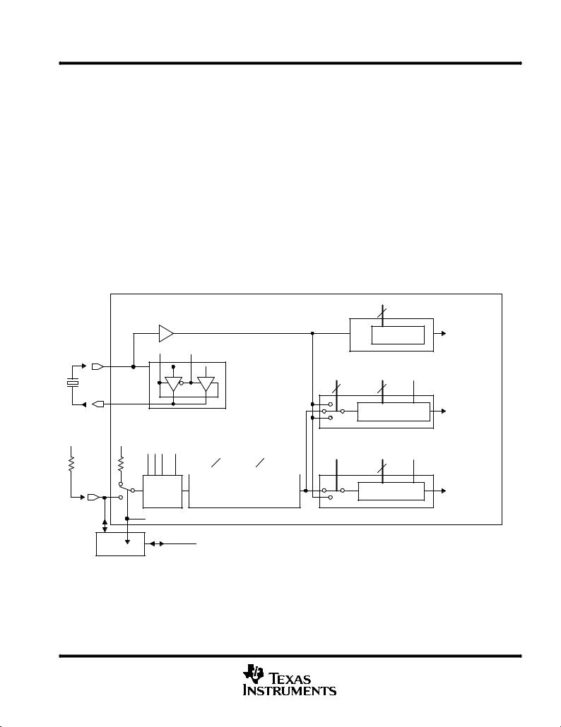
operation modes and interrupts
The MSP430 operating modes support various advanced requirements for ultra low-power and ultra low-energy consumption. This is achieved by the intelligent management of the operations during the different module operation modes and CPU states. The advanced requirements are fully supported during interrupt event handling. An interrupt event awakens the system from each of the various operating modes and returns with the RETI instruction to the mode that was selected before the interrupt event. The different requirements of the CPU and modules, which are driven by system cost and current consumption objectives, necessitate the use of different clock signals (see Figure 1):
DAuxiliary clock ACLK (from LFXTCLK/crystal's frequency), used by the peripheral modules
DMain system clock MCLK, used by the CPU and system
DSubsystem clock SMCLK, used by the peripheral modules.
|
|
DIVA |
|
|
|
2 |
|
|
LFXTCLK |
|
ACLK |
|
|
/1, /2, /4, /8 |
|
OSCOff XTS |
|
|
Auxiliary Clock |
|
|
|
|
XIN |
|
ACLKGEN |
|
High Frequency |
SELM |
DIVM CPUOff |
|
|
|
|
|
XT Oscillator, XTS=1 |
2 |
2 |
|
|
|
3 |
|
XOUT |
Low Power |
/1, /2, /4, /8, Off |
MCLK |
|
Main System Clock |
||
|
LF Oscillator, XTS = 0 |
2 |
|
|
|
MCLKGEN |
|
VCC |
VCC |
|
|
|
Rsel SCG0 |
DCO |
MOD |
|
|
|||
|
|
|
|
3 |
|
5 |
|
SELS |
DIVS |
SCG1 |
|
|
|
|
|
DCOCLK |
2 |
|
|||
|
|
|
|
|
|
|
|
|||
|
|
|
|
|
|
|
|
|
|
|
|
0 |
DC |
Digital Controlled Oscillator (DCO) |
0 |
|
|
|
|
|||
|
|
+ |
/1, /2, /4, /8, Off |
SMCLK |
|
|
|
Generator |
|||
|
|
Modulator (MOD) |
|
Sub-System Clock |
|
|
1 |
|
1 |
||
|
|
|
|||
P2.5/ROSC |
|
|
|
||
|
DCOMOD |
SMCLKGEN |
|
||
|
|
|
|||
|
|
DCOR |
|
||
|
|
|
|
|
|
|
|
|
The DCO-Generator is connected to pin P2.5/ROSC if DCOR control bit is set. |
|
|
|
|
|
The port pin P2.5/ROSC is selected if DCOR control bit is reset (initial state). |
|
|
|
P2.5 |
|
|
|
|
Figure 1. Clock Signals
POST OFFICE BOX 655303 •DALLAS, TEXAS 75265 |
5 |

MSP430x11x
MIXED SIGNAL MICROCONTROLLERS
SLAS196B± DECEMBER 1998 ± REVISED APRIL 2000
operation modes and interrupts (continued)
Two clock sources, LFXTCLK and DCOCLK, can be used to drive the MSP430 system. The LFXTCLK is defined by connecting a low power, low frequency crystal to the oscillator, by connecting a high frequency crystal to the oscillator, or by applying an external clock source. The high frequency crystal oscillator is used if the control bit XTS is set. The crystal oscillator may be switched off when the LFXTCLK oscillator is not needed for the present operation mode. The DCOCLK is active and the frequency is selected or adjusted by the software. The DCOCLK is inactive or stopped when it is not used by the CPU or peripheral modules. The dc-generator can be stopped when SCG0 is reset and DCOCLK is not needed. The dc-generator defines the basic DCO frequency and can be defined by one external resistor or it is adjusted in eight steps with the integrated resistors.
NOTE:
The system clock generator always starts with the DCOCLK selected for MCLK (CPU clock) to ensure proper start of program execution. The software then defines the final system clock, via control bit manipulation.
low-power consumption capabilities
The various operating modes are controlled by the software through controlling the operation of the internal clock system. This clock system provides many combinations of hardware and software capabilities to run the application with the lowest power consumption and with optimized system costs:
DUse the internal clock (DCO) generator without any external components.
DSelect an external crystal or ceramic resonator for lowest frequency or cost.
DSelect and activate the proper clock signals (LFXTCLK and/or DCOCLK) and clock pre-divider function.
DApply an external clock source.
Four of the control bits that influence the operation of the clock system and support fast turnon from low power operating modes are located in the status register SR. The four bits that control the CPU and the system clock generator are SCG1, SCG0, OscOff, and CPUOff:
status register R2
15 |
9 |
8 |
7 |
6 |
5 |
4 |
3 |
2 |
1 |
0 |
Reserved For Future |
|
V |
SCG1 |
SCG0 |
OscOff |
CPUOff |
GIE |
N |
Z |
C |
Enhancements |
|
|||||||||
|
|
|
|
|
|
|
|
|
|
|
|
|
|
|
|
|
|
|
|
|
|
rw-0 |
|
rw-0 |
rw-0 |
rw-0 |
rw-0 |
rw-0 |
rw-0 |
rw-0 |
rw-0 |
rw-0 |
The bits CPUOff, SCG1, SCG0, and OscOff are the most important low-power control bits when the basic function of the system clock generator is established. They are pushed onto the stack whenever an interrupt is accepted and thereby saved so that the previous mode of operation can be retrieved after the interrupt request. During execution of an interrupt handler routine, the bits can be manipulated via indirect access of the data on the stack. That allows the program to resume execution in another power operating mode after the return from interrupt (RETI).
SCG1: |
The clock signal SMCLK, used for peripherals, is enabled when the bit is reset or disabled if the |
|
bit is set. |
SCG0: |
The dc-generator is active when it is reset. The DCO can be deactivated only if the SCG0 bit is |
|
set and the DCOCLK signal is not used for MCLK or SMCLK. The current consumed by the |
|
dc-generator defines the basic frequency of the DCOCLK. It is a dc current. |
|
NOTE: |
|
When the current is switched off (SCG0=1) the start of the DCOCLK is delayed slightly. The delay |
|
is in the s-range. See device parameters for the specified values. |
|
|
|
|
6 |
POST OFFICE BOX 655303 •DALLAS, TEXAS 75265 |

|
MSP430x11x |
|
|
MIXED SIGNAL MICROCONTROLLERS |
|
|
SLAS196B± DECEMBER 1998 ± REVISED APRIL 2000 |
|
|
|
|
status register R2 (continued) |
||
OscOff: |
The LFXT crystal oscillator is active when the OscOff bit is reset. The LFXT oscillator can only be |
|
|
deactivated if the OscOff bit is set and it is not used for MCLK or SMCLK. The setup time to start |
|
|
a crystal oscillation needs consideration when the oscillator off option is used. Mask |
|
|
programmable (ROM) devices can disable this feature so that the oscillator can never be switched |
|
|
off by software. |
|
CPUOff: |
The clock signal MCLK, used for the CPU, is active when the bit is reset or stopped if it is set. |
|
DCOCLK: |
The clock signal DCOCLK is deactivated if it is not used for MCLK or SMCLK or if the SCG0 bit |
|
|
is set. There are two situations when the SCG0 bit cannot switch off the DCOCLK signal: |
|
|
1. DCOCLK frequency is used for MCLK (CPUOff=0 and SELM.1=0). |
|
|
2. DCOCLK frequency is used for SMCLK (SCG1=0 and SELS=0). |
|
interrupt vector addresses
The interrupt vectors and the power-up starting address are located in the ROM with an address range of 0FFFFh-0FFE0h. The vector contains the 16-bit address of the appropriate interrupt handler instruction sequence.
INTERRUPT SOURCE |
INTERRUPT FLAG |
SYSTEM INTERRUPT |
WORD ADDRESS |
PRIORITY |
|
|
|
|
|
|
|
Power-up, external reset, watchdog |
WDTIFG (see Note1) |
Reset |
0FFFEh |
15, highest |
|
|
|
|
|
|
|
NMI, oscillator fault |
NMIIFG, OFIFG (see Note 1) |
(non)-maskable, |
0FFFCh |
14 |
|
(non)-maskable |
|||||
|
|
|
|
||
|
|
|
|
|
|
|
|
|
0FFFAh |
13 |
|
|
|
|
|
|
|
|
|
|
0FFF8h |
12 |
|
|
|
|
|
|
|
|
|
|
0FFF6h |
11 |
|
|
|
|
|
|
|
Watchdog Timer |
WDTIFG |
maskable |
0FFF4h |
10 |
|
|
|
|
|
|
|
Timer_A |
CCIFG0 (see Note 2) |
maskable |
0FFF2h |
9 |
|
|
|
|
|
|
|
Timer_A |
CCIFG1, CCIFG2, TAIFG |
maskable |
0FFF0h |
8 |
|
(see Notes 1 and 2) |
|||||
|
|
|
|
||
|
|
|
|
|
|
|
|
|
0FFEEh |
7 |
|
|
|
|
|
|
|
|
|
|
0FFECh |
6 |
|
|
|
|
|
|
|
|
|
|
0FFEAh |
5 |
|
|
|
|
|
|
|
|
|
|
0FFE8h |
4 |
|
|
|
|
|
|
|
I/O Port P2 (eight flags ± see Note 3) |
P2IFG.0 to P2IFG.7 |
maskable |
0FFE6h |
3 |
|
(see Notes 1 and 2) |
|||||
|
|
|
|
||
|
|
|
|
|
|
I/O Port P1 (eight flags) |
P1IFG.0 to P1IFG.7 |
maskable |
0FFE4h |
2 |
|
(see Notes 1 and 2) |
|||||
|
|
|
|
||
|
|
|
|
|
|
|
|
|
0FFE2h |
1 |
|
|
|
|
|
|
|
|
|
|
0FFE0h |
0, lowest |
|
|
|
|
|
|
|
NOTES: 1. Multiple source flags |
|
|
|
|
2.Interrupt flags are located in the module
3.There are eight Port P2 interrupt flags, but only six Port P2 I/O pins (P2.0±5) are implemented on the 11x devices.
POST OFFICE BOX 655303 •DALLAS, TEXAS 75265 |
7 |

MSP430x11x
MIXED SIGNAL MICROCONTROLLERS
SLAS196B± DECEMBER 1998 ± REVISED APRIL 2000
special function registers
Most interrupt and module enable bits are collected into the lowest address space. Special function register bits that are not allocated to a functional purpose are not physically present in the device. Simple software access is provided with this arrangement.
interrupt enable 1
Address |
7 |
6 |
|
5 |
|
4 |
|
3 |
|
2 |
1 |
0 |
|
0h |
|
|
|
|
|
|
NMIIE |
|
|
|
|
OFIE |
WDTIE |
|
|
|
|
|
|
|
|
|
|
|
|
|
|
|
|
|
|
|
|
|
rw-0 |
|
|
|
rw-0 |
rw-0 |
|
WDTIE: |
Watchdog Timer enable signal |
|
|
|
|
|
|
|
|||||
OFIE: |
Oscillator fault enable signal |
|
|
|
|
|
|
|
|||||
NMIIE: |
Non-maskable interrupt enable signal |
|
|
|
|
|
|||||||
interrupt flag register 1 |
|
|
|
|
|
|
|
|
|
|
|
|
|
Address |
7 |
6 |
|
5 |
|
4 |
|
3 |
|
2 |
1 |
0 |
|
02h |
|
|
|
|
|
|
NMIIFG |
|
|
|
|
OFIFG |
WDTIFG |
|
|
|
|
|
|
|
|
|
|
|
|
|
|
|
|
|
|
|
|
|
rw-0 |
|
|
|
rw-1 |
rw-0 |
|
WDTIFG: |
Set on overflow or security key violation |
|
|
|
|
|
|||||||
|
OR |
|
|
|
|
|
|
|
|
|
|
|
|
|
Reset on VCC power-on or reset condition at RST/NMI-pin |
|
|
|
|||||||||
OFIFG: |
Flag set on oscillator fault |
|
|
|
|
|
|
|
|||||
NMIIFG: |
Set via |
|
|
|
|
|
|
|
|
|
|
|
|
RST/NMI-pin |
|
|
|
|
|
|
|
|
|
||||
Legend |
rw: |
Bit can be read and written. |
|
|
|
|
|
|
|
||||
|
rw-0: |
Bit can be read and written. It is reset by PUC |
|
|
|
|
|
||||||
|
|
SFR bit is not present in device. |
|
|
|
|
|
||||||
|
|
|
|
|
|
|
|
|
|
|
|
|
|
8 |
POST OFFICE BOX 655303 •DALLAS, TEXAS 75265 |

|
|
|
|
|
|
|
|
MSP430x11x |
||
|
|
|
|
MIXED SIGNAL MICROCONTROLLERS |
||||||
|
|
|
|
|
|
SLAS196B± DECEMBER 1998 ± REVISED APRIL 2000 |
||||
|
|
|
|
|
|
|
|
|
|
|
memory organization |
|
|
|
|
|
|
|
|
|
|
|
|
|
|
|
|
MSP430P112 |
||||
|
MSP430C111 |
|
MSP430C112 |
|
|
PMS430E112 |
||||
FFFFh |
|
FFFFh |
|
FFFFh |
|
|
|
|||
Int. Vector |
Int. Vector |
Int. Vector |
||||||||
FFE0h |
FFE0h |
FFE0h |
||||||||
|
|
|
|
|
||||||
FFDFh |
2 kB ROM |
FFDFh |
|
FFDFh |
||||||
|
|
|
|
|
4 kB |
|||||
F800h |
|
|
4 kB ROM |
|
|
|||||
|
|
|
|
EPROM |
||||||
|
|
|
|
|
|
|||||
|
|
F000h |
|
F000h |
|
|
||||
027Fh |
|
02FFh |
|
|
|
02FFh |
|
|
|
|
|
|
|
|
|
||
128B RAM |
0200h |
256B RAM |
0200h |
256B RAM |
||||
0200h |
||||||||
|
|
|
|
|||||
01FFh |
16b Per. |
01FFh |
16b Per. |
01FFh |
16b Per. |
|||
0100h |
0100h |
0100h |
||||||
|
|
|
|
|||||
00FFh |
8b Per. |
00FFh |
8b Per. |
00FFh |
8b Per. |
|||
0010h |
0010h |
0010h |
||||||
|
|
|
|
|||||
000Fh |
SFR |
000Fh |
SFR |
000Fh |
SFR |
|||
0000h |
|
0000h |
|
|
0000h |
|
||
|
|
|
|
|||||
peripherals
Peripherals are connected to the CPU through data, address, and control buses and can be handled easily with instructions for memory manipulation.
digital I/O
There are two eight-bit I/O ports, Port P1 and Port P2 ± implemented (11x parts only have six Port P2 I/O signals available on external pins). Both ports, P1 and P2, have seven control registers to give maximum flexibility of digital input/output to the application:
•All individual I/O bits are programmable independently.
•Any combination of input, output, and interrupt conditions is possible.
•Interrupt processing of external events is fully implemented for all eight bits of port P1 and for six bits of Port P2.
•Provides read/write access to all registers with all instructions.
The seven registers are: |
|
|
• Input register |
8 bits at Port P1/P2 |
contains information at the pins |
• Output register |
8 bits at Port P1/P2 |
contains output information |
• Direction register |
8 bits at Port P1/P2 |
controls direction |
• Interrupt edge select |
8 bits at Port P1/P2 |
input signal change necessary for interrupt |
• Interrupt flags |
8 bits at Port P1/P2 |
indicates if interrupt(s) are pending |
• Interrupt enable |
8 bits at Port P1/P2 |
contains interrupt enable bits |
• Selection (Port or Mod.) 8 bits at Port P1/P2 |
determines if pin(s) have port or module function |
|
|
|
|
|
|
|
POST OFFICE BOX 655303 •DALLAS, TEXAS 75265 |
9 |
 Loading...