


 Loading...
Texas Instruments LM340MP, LM340MPX, LM340AT, LM340K, LM340S Schematic [ru]
...LM340-N, LM78xx
www.ti.com |
SNOSBT0J –FEBRUARY 2000–REVISED DECEMBER 2013 |
LM340-N/LM78XX Series 3-Terminal Positive Regulators
Check for Samples: LM340-N, LM78xx
FEATURES
•Complete Specifications at 1A Load
•Output Voltage Tolerances of ±2% at Tj = 25°C and ±4% Over the Temperature Range (LM340A)
• Line Regulation of 0.01% of VOUT/V of VIN at 1A Load (LM340A)
•Load Regulation of 0.3% of VOUT/A (LM340A)
•Internal Thermal Overload Protection
•Internal Short-circuit Current Limit
•Output Transistor Safe Area Protection
•P+ Product Enhancement Tested
DESCRIPTION
The LM140/LM340A/LM340-N/LM78XXC monolithic 3-terminal positive voltage regulators employ internal current-limiting, thermal shutdown and safe-area compensation, making them essentially indestructible. If adequate heat sinking is provided, they can deliver over 1.0A output current. They are intended as fixed voltage regulators in a wide range of applications including local (on-card) regulation for elimination of noise and distribution problems associated with single-point regulation. In addition to use as fixed voltage regulators, these devices can be used with external components to obtain adjustable output voltages and currents.
Considerable effort was expended to make the entire series of regulators easy to use and minimize the number of external components. It is not necessary to bypass the output, although this does improve transient response. Input bypassing is needed only if the regulator is located far from the filter capacitor of the power supply.
The 5V, 12V, and 15V regulator options are available in the steel TO-3 power package. The LM340A/LM340-N/LM78XXC series is available in the TO-220 plastic power package, and the LM340-N-5.0 is available in the SOT-223 package, as well as the LM340-5.0 and LM340-12 in the surface-mount DDPAK/TO-263 package.
Typical Applications
*Required if the regulator is located far from the power supply filter. |
|
**Although no output capacitor is needed for stability, it does help |
|
transient response. (If needed, use 0.1 μF, ceramic disc). |
VOUT = 5V + (5V/R1 + IQ) R2 5V/R1 > 3 IQ, |
|
load regulation (Lr) ≈ [(R1 + R2)/R1] (Lr of LM340-5). |
Figure 1. Fixed Output Regulator |
Figure 2. Adjustable Output Regulator |
Please be aware that an important notice concerning availability, standard warranty, and use in critical applications of
 Texas Instruments semiconductor products and disclaimers thereto appears at the end of this data sheet. All trademarks are the property of their respective owners.
PRODUCTION DATA information is current as of publication date. |
Copyright © 2000–2013, Texas Instruments Incorporated |
Products conform to specifications per the terms of the Texas |
|
Instruments standard warranty. Production processing does not |
|
necessarily include testing of all parameters. |
|

LM340-N, LM78xx
SNOSBT0J –FEBRUARY 2000 –REVISED DECEMBER 2013 |
www.ti.com |
SOT-223 DDPAK/TO-263
IQ = 1.3 mA over line and load changes. |
|
Figure 3. Current Regulator |
Figure 4. Comparison between SOT-223 and |
|
DDPAK/TO-263 Packages |
|
Scale 1:1 |
Connection Diagrams
Figure 5. DDPAK/TO-263 Surface-Mount Package |
Figure 6. 3-Lead SOT-223 |
Top View |
Top View |
See Package Number KTT0003B |
See Package Number DCY |
These devices have limited built-in ESD protection. The leads should be shorted together or the device placed in conductive foam during storage or handling to prevent electrostatic damage to the MOS gates.
Absolute Maximum Ratings(1)(2)(3)
DC Input Voltage |
|
35V |
Internal Power Dissipation(4) |
|
Internally Limited |
Maximum Junction Temperature |
|
150°C |
Storage Temperature Range |
|
−65°C to +150°C |
Lead Temperature (Soldering, 10 sec.) |
TO-3 Package (NDS) |
300°C |
|
TO-220 Package (NDE), DDPAK/TO-263 |
|
|
Package (KTT) |
230°C |
ESD Susceptibility(5) |
|
2 kV |
(1)Absolute Maximum Ratings are limits beyond which damage to the device may occur. Operating Conditions are conditions under which the device functions but the specifications might not be ensured. For ensured specifications and test conditions see the Electrical Characteristics.
(2)Military datasheets are available upon request. At the time of printing, the military datasheet specifications for the LM140K-5.0/883, LM140K-12/883, and LM140K-15/883 complied with the min and max limits for the respective versions of the LM140. The LM140H and LM140K may also be procured as JAN devices on slash sheet JM38510/107.
(3)If Military/Aerospace specified devices are required, please contact the Texas Instruments Sales Office/Distributors for availability and specifications.
(4)The maximum allowable power dissipation at any ambient temperature is a function of the maximum junction temperature for operation
(TJMAX = 125°C or 150°C), the junction-to-ambient thermal resistance (θJA), and the ambient temperature (TA). PDMAX = (TJMAX − TA)/θJA. If this dissipation is exceeded, the die temperature will rise above TJMAX and the electrical specifications do not apply. If the die temperature rises above 150°C, the device will go into thermal shutdown. For the TO-3 package (NDS), the junction-to-ambient thermal
resistance (θJA) is 39°C/W. When using a heatsink, θJA is the sum of the 4°C/W junction-to-case thermal resistance (θJC) of the TO-3 package and the case-to-ambient thermal resistance of the heatsink. For the TO-220 package (NDE), θJA is 54°C/W and θJC is 4°C/W. If SOT-223 is used, the junction-to-ambient thermal resistance is 174°C/W and can be reduced by a heatsink (see Applications Hints on heatsinking).If the DDPAK\TO-263 package is used, the thermal resistance can be reduced by increasing the PC board copper area
thermally connected to the package: Using 0.5 square inches of copper area, θJA is 50°C/W; with 1 square inch of copper area, θJAis 37°C/W; and with 1.6 or more inches of copper area, θJA is 32°C/W.
(5)ESD rating is based on the human body model, 100 pF discharged through 1.5 kΩ.
Operating Conditions(1)
(1)Absolute Maximum Ratings are limits beyond which damage to the device may occur. Operating Conditions are conditions under which the device functions but the specifications might not be ensured. For ensured specifications and test conditions see the Electrical Characteristics.
2 |
Submit Documentation Feedback |
Copyright © 2000–2013, Texas Instruments Incorporated |
Product Folder Links: LM340-N LM78xx

|
|
|
|
LM340-N, LM78xx |
www.ti.com |
|
|
SNOSBT0J –FEBRUARY 2000–REVISED DECEMBER 2013 |
|
Operating Conditions(1) |
(continued) |
|
|
|
|
|
LM140 |
|
−55°C to +125°C |
Temperature Range (TA)(2) |
|
LM340A, LM340-N |
|
0°C to +125°C |
|
|
LM7808C |
|
0°C to +125°C |
(2)The maximum allowable power dissipation at any ambient temperature is a function of the maximum junction temperature for operation
(TJMAX = 125°C or 150°C), the junction-to-ambient thermal resistance (θJA), and the ambient temperature (TA). PDMAX = (TJMAX − TA)/θJA. If this dissipation is exceeded, the die temperature will rise above TJMAX and the electrical specifications do not apply. If the die temperature rises above 150°C, the device will go into thermal shutdown. For the TO-3 package (NDS), the junction-to-ambient thermal
resistance (θJA) is 39°C/W. When using a heatsink, θJA is the sum of the 4°C/W junction-to-case thermal resistance (θJC) of the TO-3 package and the case-to-ambient thermal resistance of the heatsink. For the TO-220 package (NDE), θJA is 54°C/W and θJC is 4°C/W. If SOT-223 is used, the junction-to-ambient thermal resistance is 174°C/W and can be reduced by a heatsink (see Applications Hints on heatsinking).If the DDPAK\TO-263 package is used, the thermal resistance can be reduced by increasing the PC board copper area
thermally connected to the package: Using 0.5 square inches of copper area, θJA is 50°C/W; with 1 square inch of copper area, θJAis 37°C/W; and with 1.6 or more inches of copper area, θJA is 32°C/W.
Copyright © 2000–2013, Texas Instruments Incorporated |
Submit Documentation Feedback |
3 |
Product Folder Links: LM340-N LM78xx

LM340-N, LM78xx
SNOSBT0J –FEBRUARY 2000 –REVISED DECEMBER 2013 www.ti.com
LM340A Electrical Characteristics
IOUT = 1A, 0°C ≤ TJ ≤ + 125°C (LM340A) unless otherwise specified(1)
|
|
Output Voltage |
|
5V |
|
|
12V |
|
|
15V |
|
|
|
Symbol |
Input Voltage (unless otherwise noted) |
|
10V |
|
|
19V |
|
|
23V |
|
Units |
||
|
Parameter |
Conditions |
Min |
Typ |
Max |
Min |
Typ |
Max |
Min |
Typ |
Max |
|
|
VO |
Output |
TJ = 25°C |
|
4.9 |
5 |
5.1 |
11.75 |
12 |
12.25 |
14.7 |
15 |
15.3 |
V |
|
Voltage |
PD ≤ 15W, 5 mA ≤ IO ≤ 1A |
4.8 |
|
5.2 |
11.5 |
|
12.5 |
14.4 |
|
15.6 |
V |
|
|
|
|
|
|
|||||||||
|
|
VMIN ≤ VIN ≤ VMAX |
(7.5 ≤ VIN ≤ 20) |
(14.8 ≤ VIN ≤ 27) |
(17.9 ≤ VIN ≤ 30) |
V |
|||||||
VO |
Line |
IO = 500 mA |
|
|
10 |
|
|
18 |
|
|
22 |
mV |
|
|
Regulation |
VIN |
|
(7.5 ≤ VIN ≤ 20) |
(14.8 ≤ VIN ≤ 27) |
(17.9 ≤ VIN ≤ 30) |
V |
||||||
|
|
|
|||||||||||
|
|
TJ = 25°C |
|
|
3 |
10 |
|
4 |
18 |
|
4 |
22 |
mV |
|
|
VIN |
|
(7.5 ≤ VIN ≤ 20) |
(14.5 ≤ VIN ≤ 27) |
(17.5 ≤ VIN ≤ 30) |
V |
||||||
|
|
TJ = 25°C |
|
|
|
4 |
|
|
9 |
|
|
10 |
mV |
|
|
Over Temperature |
|
|
12 |
|
|
30 |
|
|
30 |
mV |
|
|
|
VIN |
|
(8 ≤ VIN ≤ 12) |
(16 ≤ VIN ≤ 22) |
(20 ≤ VIN ≤ 26) |
V |
||||||
VO |
Load |
TJ = |
5 mA ≤ IO ≤ 1.5A |
|
10 |
25 |
|
12 |
32 |
|
12 |
35 |
mV |
|
Regulation |
25°C |
250 mA ≤ IO ≤ |
|
|
15 |
|
|
19 |
|
|
21 |
mV |
|
|
|
|
|
|
|
|
|
|||||
|
|
|
750 mA |
|
|
|
|
|
|
|
|
|
|
|
|
Over Temperature, |
|
|
25 |
|
|
60 |
|
|
75 |
mV |
|
|
|
5 mA ≤ IO ≤ 1A |
|
|
|
|
|
|
|
|
|
|
|
IQ |
Quiescent |
TJ = 25°C |
|
|
|
6 |
|
|
6 |
|
|
6 |
mA |
|
Current |
Over Temperature |
|
|
6.5 |
|
|
6.5 |
|
|
6.5 |
mA |
|
|
|
|
|
|
|
|
|
||||||
IQ |
Quiescent |
5 mA ≤ IO ≤ 1A |
|
|
0.5 |
|
|
0.5 |
|
|
0.5 |
mA |
|
|
Current |
|
|
|
|
|
|
|
|
|
|
|
|
|
TJ = 25°C, IO = 1A |
|
|
0.8 |
|
|
0.8 |
|
|
0.8 |
mA |
||
|
Change |
|
|
|
|
|
|
||||||
|
|
VMIN ≤ VIN ≤ VMAX |
(7.5 ≤ VIN ≤ 20) |
(14.8 ≤ VIN ≤ 27) |
(17.9 ≤ VIN ≤ 30) |
V |
|||||||
|
|
IO = 500 mA |
|
|
0.8 |
|
|
0.8 |
|
|
0.8 |
mA |
|
|
|
VMIN ≤ VIN ≤ VMAX |
(8 ≤ VIN ≤ 25) |
(15 ≤ VIN ≤ 30) |
(17.9 ≤ VIN ≤ 30) |
V |
|||||||
VN |
Output Noise |
TA = 25°C, 10 Hz ≤ f ≤ 100 |
|
40 |
|
|
75 |
|
|
90 |
|
μV |
|
|
Voltage |
kHz |
|
|
|
|
|
|
|
|
|
|
|
|
Ripple |
TJ = 25°C, f = 120 Hz, IO = |
68 |
80 |
|
61 |
72 |
|
60 |
70 |
|
dB |
|
|
Rejection |
1A |
|
|
|
|
|
|
|
|
|
|
|
|
|
or f = 120 Hz, IO = 500 mA, |
68 |
|
|
61 |
|
|
60 |
|
|
dB |
|
|
|
Over Temperature, |
|
|
|
|
|
|
|
|
|
|
|
|
|
VMIN ≤ VIN ≤ VMAX |
(8 ≤ VIN ≤ 18) |
(15 ≤ VIN ≤ 25) |
(18.5 ≤ VIN ≤ 28.5) |
V |
|||||||
RO |
Dropout |
TJ = 25°C, IO = 1A |
|
2.0 |
|
|
2.0 |
|
|
2.0 |
|
V |
|
|
Voltage |
|
|
|
|
|
|
|
|
|
|
|
|
|
Output |
f = 1 kHz |
|
|
8 |
|
|
18 |
|
|
19 |
|
mΩ |
|
Resistance |
|
|
|
|
|
|
|
|
|
|
|
|
|
Short-Circuit |
TJ = 25°C |
|
|
2.1 |
|
|
1.5 |
|
|
1.2 |
|
A |
|
Current |
|
|
|
|
|
|
|
|
|
|
|
|
|
Peak Output |
TJ = 25°C |
|
|
2.4 |
|
|
2.4 |
|
|
2.4 |
|
A |
|
Current |
|
|
|
|
|
|
|
|
|
|
|
|
|
Average TC |
Min, TJ = 0°C, IO = 5 mA |
|
−0.6 |
|
|
−1.5 |
|
|
−1.8 |
|
mV/°C |
|
|
of VO |
|
|
|
|
|
|
|
|
|
|
|
|
VIN |
Input Voltage |
TJ = 25°C |
|
|
|
|
|
|
|
|
|
|
|
|
Required to |
|
|
7.5 |
|
|
14.5 |
|
|
17.5 |
|
|
V |
|
Maintain Line |
|
|
|
|
|
|
|
|
||||
|
|
|
|
|
|
|
|
|
|
|
|
|
|
|
Regulation |
|
|
|
|
|
|
|
|
|
|
|
|
(1)All characteristics are measured with a 0.22 μF capacitor from input to ground and a 0.1 μF capacitor from output to ground. All
characteristics except noise voltage and ripple rejection ratio are measured using pulse techniques (tw ≤ 10 ms, duty cycle ≤ 5%). Output voltage changes due to changes in internal temperature must be taken into account separately.
4 |
Submit Documentation Feedback |
Copyright © 2000–2013, Texas Instruments Incorporated |
Product Folder Links: LM340-N LM78xx

|
|
|
|
|
|
|
|
|
|
|
|
LM340-N, LM78xx |
||
www.ti.com |
|
|
|
|
|
|
SNOSBT0J –FEBRUARY 2000–REVISED DECEMBER 2013 |
|||||||
LM140 Electrical Characteristics(1) |
|
|
|
|
|
|
|
|
|
|
||||
−55°C ≤ TJ ≤ +150°C unless otherwise specified |
|
|
|
|
|
|
|
|
|
|
||||
Symb |
Output Voltage |
|
5V |
|
|
12V |
|
|
15V |
|
|
|||
Input Voltage (unless otherwise noted) |
|
10V |
|
|
19V |
|
|
23V |
|
Units |
||||
ol |
|
|
|
|
|
|
||||||||
Parameter |
Conditions |
Min |
Typ |
Max |
Min |
Typ |
Max |
Min |
Typ |
Max |
|
|||
|
|
|||||||||||||
VO |
Output Voltage |
TJ = 25°C, 5 mA ≤ IO ≤ 1A |
4.8 |
5 |
5.2 |
11.5 |
12 |
12.5 |
14.4 |
15 |
15.6 |
V |
||
|
|
PD ≤ 15W, 5 mA ≤ IO ≤ 1A |
4.75 |
|
5.25 |
11.4 |
|
12.6 |
14.25 |
|
15.75 |
V |
||
|
|
VMIN ≤ VIN ≤ VMAX |
(8 ≤ VIN ≤ 20) |
(15.5 ≤ VIN ≤ 27) |
(18.5 ≤ VIN ≤ 30) |
V |
||||||||
VO |
Line |
IO = 500 |
|
TJ = 25°C |
|
3 |
50 |
|
4 |
120 |
|
4 |
150 |
mV |
|
Regulation |
mA |
|
|
|
|
|
|
|
|
|
|
|
|
|
|
VIN |
(7 ≤ VIN ≤ 25) |
(14.5 ≤ VIN ≤ 30) |
(17.5 ≤ VIN ≤ 30) |
V |
||||||||
|
|
|
|
|||||||||||
|
|
|
|
−55°C ≤ TJ ≤ |
|
|
50 |
|
|
120 |
|
|
150 |
mV |
|
|
|
|
+150°C |
|
|
|
|
|
|
|
|
|
|
|
|
|
|
VIN |
(8 ≤ VIN ≤ 20) |
(15 ≤ VIN ≤ 27) |
(18.5 ≤ VIN ≤ 30) |
V |
||||||
|
|
IO ≤ 1A |
|
TJ = 25°C |
|
|
50 |
|
|
120 |
|
|
150 |
mV |
|
|
|
|
VIN |
(7.5 ≤ VIN ≤ 20) |
(14.6 ≤ VIN ≤ 27) |
(17.7 ≤ VIN ≤ 30) |
V |
||||||
|
|
|
|
−55°C ≤ TJ ≤ |
|
|
25 |
|
|
60 |
|
|
75 |
mV |
|
|
|
|
+150°C |
|
|
|
|
|
|
|
|
|
|
|
|
|
|
VIN |
(8 ≤ VIN ≤ 12) |
(16 ≤ VIN ≤ 22) |
(20 ≤ VIN ≤ 26) |
V |
||||||
VO |
Load |
TJ = |
|
5 mA ≤ IO ≤ |
|
10 |
50 |
|
12 |
120 |
|
12 |
150 |
mV |
|
Regulation |
25°C |
|
1.5A |
|
|
|
|
|
|
|
|
|
|
|
|
|
|
250 mA ≤ IP ≤ |
|
|
25 |
|
|
60 |
|
|
75 |
mV |
|
|
|
|
750 mA |
|
|
|
|
|
|
|
|
|
|
|
|
−55°C ≤ TJ ≤ +150°C, |
|
|
50 |
|
|
120 |
|
|
150 |
mV |
||
|
|
5 mA ≤ IO ≤ 1A |
|
|
|
|
|
|
|
|
|
|
||
IQ |
Quiescent |
IO ≤ 1A |
|
TJ = 25°C |
|
|
6 |
|
|
6 |
|
|
6 |
mA |
|
Current |
|
|
−55°C ≤ TJ ≤ |
|
|
7 |
|
|
7 |
|
|
7 |
mA |
|
|
|
|
|
|
|
|
|
|
|||||
|
|
|
|
+150°C |
|
|
|
|
|
|
|
|
|
|
IQ |
Quiescent |
5 mA ≤ IO ≤ 1A |
|
0.5 |
|
|
0.5 |
|
|
0.5 |
|
mA |
||
|
Current |
TJ = 25°C, IO ≤ 1A |
|
|
0.8 |
|
|
0.8 |
|
|
0.8 |
mA |
||
|
Change |
|
|
|
|
|
|
|||||||
|
|
VMIN ≤ VIN ≤ VMAX |
(8 ≤ VIN ≤ 20) |
(15 ≤ VIN ≤ 27) |
(18.5 ≤ VIN ≤ 30) |
V |
||||||||
|
|
IO = 500 mA, −55°C ≤ TJ ≤ |
|
|
0.8 |
|
|
0.8 |
|
|
0.8 |
mA |
||
|
|
+150°C |
|
|
|
|
|
|
|
|
|
|
|
|
|
|
VMIN ≤ VIN ≤ VMAX |
(8 ≤ VIN ≤ 25) |
(15 ≤ VIN ≤ 30) |
(18.5 ≤ VIN ≤ 30) |
V |
||||||||
VN |
Output Noise |
TA = 25°C, |
10 Hz ≤ f ≤ 100 |
|
40 |
|
|
75 |
|
|
90 |
|
μV |
|
|
Voltage |
kHz |
|
|
|
|
|
|
|
|
|
|
|
|
|
Ripple |
f = 120 |
|
IO ≤ 1A, TJ = |
68 |
80 |
|
61 |
72 |
|
60 |
70 |
|
dB |
|
Rejection |
Hz |
|
25°C or |
|
|
|
|
|
|
|
|
|
|
|
|
|
|
IO ≤ 500 mA, |
68 |
|
|
61 |
|
|
60 |
|
|
dB |
|
|
|
|
−55°C ≤ TJ |
|
|
|
|
|
|
|
|
|
|
|
|
|
|
≤+150°C |
|
|
|
|
|
|
|
|
|
|
|
|
VMIN ≤ VIN ≤ VMAX |
(8 ≤ VIN ≤ 18) |
(15 ≤ VIN ≤ 25) |
(18.5 ≤ VIN ≤ 28.5) |
V |
||||||||
RO |
Dropout |
TJ = 25°C, IO = 1A |
|
2.0 |
|
|
2.0 |
|
|
2.0 |
|
V |
||
|
Voltage |
|
|
|
|
|
|
|
|
|
|
|
|
|
|
Output |
f = 1 kHz |
|
|
8 |
|
|
18 |
|
|
19 |
|
mΩ |
|
|
Resistance |
|
|
|
|
|
|
|
|
|
|
|
|
|
|
Short-Circuit |
TJ = 25°C |
|
|
2.1 |
|
|
1.5 |
|
|
1.2 |
|
A |
|
|
Current |
|
|
|
|
|
|
|
|
|
|
|
|
|
|
Peak Output |
TJ = 25°C |
|
|
2.4 |
|
|
2.4 |
|
|
2.4 |
|
A |
|
|
Current |
|
|
|
|
|
|
|
|
|
|
|
|
|
|
Average TC of |
0°C ≤ TJ ≤ +150°C, IO = 5 |
|
−0.6 |
|
|
−1.5 |
|
|
−1.8 |
|
mV/°C |
||
|
VOUT |
mA |
|
|
|
|
|
|
|
|
|
|
|
|
(1)All characteristics are measured with a 0.22 μF capacitor from input to ground and a 0.1 μF capacitor from output to ground. All
characteristics except noise voltage and ripple rejection ratio are measured using pulse techniques (tw ≤ 10 ms, duty cycle ≤ 5%). Output voltage changes due to changes in internal temperature must be taken into account separately.
Copyright © 2000–2013, Texas Instruments Incorporated |
Submit Documentation Feedback |
5 |
Product Folder Links: LM340-N LM78xx

LM340-N, LM78xx
SNOSBT0J –FEBRUARY 2000 –REVISED DECEMBER 2013 www.ti.com
LM140 Electrical Characteristics(1) (continued)
−55°C ≤ TJ ≤ +150°C unless otherwise specified
Symb |
|
Output Voltage |
|
5V |
|
|
12V |
|
|
15V |
|
|
|
Input Voltage (unless otherwise noted) |
|
10V |
|
|
19V |
|
|
23V |
|
Units |
|||
ol |
|
|
|
|
|
|
|||||||
Parameter |
|
Conditions |
Min |
Typ |
Max |
Min |
Typ |
Max |
Min |
Typ |
Max |
|
|
|
|
|
|||||||||||
VIN |
Input Voltage |
|
TJ = 25°C, IO ≤ 1A |
|
|
|
|
|
|
|
|
|
|
|
Required to |
|
|
7.5 |
|
|
14.6 |
|
|
17.7 |
|
|
V |
|
Maintain Line |
|
|
|
|
|
|
|
|
||||
|
|
|
|
|
|
|
|
|
|
|
|
|
|
|
Regulation |
|
|
|
|
|
|
|
|
|
|
|
|
LM340-N Electrical Characteristics(1)
0°C ≤ TJ ≤ +125°C unless otherwise specified
|
Output Voltage |
|
5V |
|
|
12V |
|
|
15V |
|
|
||
Symbol |
Input Voltage (unless otherwise noted) |
|
10V |
|
|
19V |
|
|
23V |
|
Units |
||
|
Parameter |
Conditions |
Min |
Typ |
Max |
Min |
Typ |
Max |
Min |
Typ |
Max |
|
|
VO |
Output Voltage |
TJ = 25°C, 5 mA ≤ IO ≤ 1A |
4.8 |
5 |
5.2 |
11.5 |
12 |
12.5 |
14.4 |
15 |
15.6 |
V |
|
|
|
PD ≤ 15W, 5 mA ≤ IO ≤ 1A |
4.75 |
|
5.25 |
11.4 |
|
12.6 |
14.25 |
|
15.75 |
V |
|
|
|
VMIN ≤ VIN ≤ VMAX |
(7.5 ≤ VIN ≤ 20) |
(14.5 ≤ VIN ≤ 27) |
(17.5 ≤ VIN ≤ 30) |
V |
|||||||
VO |
Line Regulation |
IO = 500 |
TJ = 25°C |
|
3 |
50 |
|
4 |
120 |
|
4 |
150 |
mV |
|
|
mA |
VIN |
(7 ≤ VIN ≤ 25) |
(14.5 ≤ VIN ≤ 30) |
(17.5 ≤ VIN ≤ 30) |
V |
||||||
|
|
|
|||||||||||
|
|
|
0°C ≤ TJ ≤ |
|
|
50 |
|
|
120 |
|
|
150 |
mV |
|
|
|
+125°C |
|
|
|
|
|
|
|
|
|
|
|
|
|
VIN |
(8 ≤ VIN ≤ 20) |
(15 ≤ VIN ≤ 27) |
(18.5 ≤ VIN ≤ 30) |
V |
||||||
|
|
IO ≤ 1A |
TJ = 25°C |
|
|
50 |
|
|
120 |
|
|
150 |
mV |
|
|
|
VIN |
(7.5 ≤ VIN ≤ 20) |
(14.6 ≤ VIN ≤ 27) |
(17.7 ≤ VIN ≤ 30) |
V |
||||||
|
|
|
0°C ≤ TJ ≤ |
|
|
25 |
|
|
60 |
|
|
75 |
mV |
|
|
|
+125°C |
|
|
|
|
|
|
|
|
|
|
|
|
|
VIN |
(8 ≤ VIN ≤ 12) |
(16 ≤ VIN ≤ 22) |
(20 ≤ VIN ≤ 26) |
V |
||||||
VO |
Load Regulation |
TJ = |
5 mA ≤ IO ≤ |
|
10 |
50 |
|
12 |
120 |
|
12 |
150 |
mV |
|
|
25°C |
1.5A |
|
|
|
|
|
|
|
|
|
|
|
|
|
250 mA ≤ IO ≤ |
|
|
25 |
|
|
60 |
|
|
75 |
mV |
|
|
|
750 mA |
|
|
|
|
|
|
|
|
|
|
|
|
5 mA ≤ IO ≤ 1A, 0°C ≤ TJ |
|
|
50 |
|
|
120 |
|
|
150 |
mV |
|
|
|
≤ +125°C |
|
|
|
|
|
|
|
|
|
|
|
IQ |
Quiescent |
IO ≤ 1A |
TJ = 25°C |
|
|
8 |
|
|
8 |
|
|
8 |
mA |
|
Current |
|
0°C ≤ TJ ≤ |
|
|
8.5 |
|
|
8.5 |
|
|
8.5 |
mA |
|
|
|
|
|
|
|
|
|
|||||
|
|
|
+125°C |
|
|
|
|
|
|
|
|
|
|
IQ |
Quiescent |
5 mA ≤ IO ≤ 1A |
|
0.5 |
|
|
0.5 |
|
|
0.5 |
|
mA |
|
|
Current Change |
|
|
|
|
|
|
|
|
|
|
|
|
|
TJ = 25°C, IO ≤ 1A |
|
|
1.0 |
|
|
1.0 |
|
|
1.0 |
mA |
||
|
|
VMIN ≤ VIN ≤ VMAX |
(7.5 ≤ VIN ≤ 20) |
(14.8 ≤ VIN ≤ 27) |
(17.9 ≤ VIN ≤ 30) |
V |
|||||||
|
|
IO ≤ 500 mA, 0°C ≤ TJ ≤ |
|
|
1.0 |
|
|
1.0 |
|
|
1.0 |
mA |
|
|
|
+125°C |
|
|
|
|
|
|
|
|
|
|
|
|
|
VMIN ≤ VIN ≤ VMAX |
(7 ≤ VIN ≤ 25) |
(14.5 ≤ VIN ≤ 30) |
(17.5 ≤ VIN ≤ 30) |
V |
|||||||
VN |
Output Noise |
TA = 25°C, 10 Hz ≤ f ≤ |
|
40 |
|
|
75 |
|
|
90 |
|
μV |
|
|
Voltage |
100 kHz |
|
|
|
|
|
|
|
|
|
|
|
|
Ripple Rejection |
|
IO ≤ 1A, TJ = |
62 |
80 |
|
55 |
72 |
|
54 |
70 |
|
dB |
|
|
|
25°C |
|
|
|
|
|
|
|
|
|
|
|
|
f = 120 |
or IO ≤ 500 |
62 |
|
|
55 |
|
|
54 |
|
|
dB |
|
|
Hz |
mA, |
|
|
|
|
|
|
|
|
|
|
|
|
|
0°C ≤ TJ ≤ |
|
|
|
|
|
|
|
|
|
|
|
|
|
+125°C |
|
|
|
|
|
|
|
|
|
|
|
|
VMIN ≤ VIN ≤ VMAX |
(8 ≤ VIN ≤ 18) |
(15 ≤ VIN ≤ 25) |
(18.5 ≤ VIN ≤ 28.5) |
V |
|||||||
(1)All characteristics are measured with a 0.22 μF capacitor from input to ground and a 0.1 μF capacitor from output to ground. All
characteristics except noise voltage and ripple rejection ratio are measured using pulse techniques (tw ≤ 10 ms, duty cycle ≤ 5%). Output voltage changes due to changes in internal temperature must be taken into account separately.
6 |
Submit Documentation Feedback |
Copyright © 2000–2013, Texas Instruments Incorporated |
Product Folder Links: LM340-N LM78xx

LM340-N, LM78xx
www.ti.com SNOSBT0J –FEBRUARY 2000–REVISED DECEMBER 2013
LM340-N Electrical Characteristics(1) (continued)
0°C ≤ TJ ≤ +125°C unless otherwise specified
|
Output Voltage |
|
5V |
|
|
12V |
|
|
15V |
|
|
|
Symbol |
Input Voltage (unless otherwise noted) |
|
10V |
|
|
19V |
|
|
23V |
|
Units |
|
|
Parameter |
Conditions |
Min |
Typ |
Max |
Min |
Typ |
Max |
Min |
Typ |
Max |
|
RO |
Dropout Voltage |
TJ = 25°C, IO = 1A |
|
2.0 |
|
|
2.0 |
|
|
2.0 |
|
V |
|
Output |
f = 1 kHz |
|
8 |
|
|
18 |
|
|
19 |
|
mΩ |
|
Resistance |
|
|
|
|
|
|
|
|
|
|
|
|
Short-Circuit |
TJ = 25°C |
|
2.1 |
|
|
1.5 |
|
|
1.2 |
|
A |
|
Current |
|
|
|
|
|
|
|
|
|
|
|
|
Peak Output |
TJ = 25°C |
|
2.4 |
|
|
2.4 |
|
|
2.4 |
|
A |
|
Current |
|
|
|
|
|
|
|
|
|
|
|
|
Average TC of |
0°C ≤ TJ ≤ +125°C, IO = 5 |
|
−0.6 |
|
|
−1.5 |
|
|
−1.8 |
|
mV/°C |
|
VOUT |
mA |
|
|
|
|
|
|
|
|
|
|
VIN |
Input Voltage |
TJ = 25°C, IO ≤ 1A |
|
|
|
|
|
|
|
|
|
|
|
Required to |
|
7.5 |
|
|
14.6 |
|
|
17.7 |
|
|
V |
|
Maintain Line |
|
|
|
|
|
|
|
||||
|
|
|
|
|
|
|
|
|
|
|
|
|
|
Regulation |
|
|
|
|
|
|
|
|
|
|
|
LM7808C
Electrical Characteristics
0°C ≤ TJ ≤ +150°C, VI = 14V, IO = 500 mA, CI = 0.33 μF, CO = 0.1 μF, unless otherwise specified
Symbol |
Parameter |
|
|
Conditions(1) |
|
LM7808C |
|
Units |
||||
|
|
|
|
|
|
|
Min |
|
Typ |
|
Max |
|
VO |
Output Voltage |
|
TJ = 25°C |
|
|
7.7 |
|
8.0 |
|
8.3 |
V |
|
VO |
Line Regulation |
|
TJ = 25°C |
|
10.5V ≤ VI ≤ 25V |
|
|
6.0 |
|
160 |
mV |
|
|
|
|
|
|
|
11.0V ≤ VI ≤ 17V |
|
|
2.0 |
|
80 |
|
VO |
Load Regulation |
|
TJ = 25°C |
|
5.0 mA ≤ IO ≤ 1.5A |
|
|
12 |
|
160 |
mV |
|
|
|
|
|
|
|
250 mA ≤ IO ≤ 750 mA |
|
|
4.0 |
|
80 |
|
VO |
Output Voltage |
|
11.5V ≤ VI ≤ 23V, 5.0 mA ≤ IO ≤ 1.0A, P ≤ 15W |
7.6 |
|
|
|
8.4 |
V |
|||
IQ |
Quiescent Current |
|
TJ = 25°C |
|
|
|
|
4.3 |
|
8.0 |
mA |
|
IQ |
Quiescent |
|
With Line |
11.5V ≤ VI ≤ 25V |
|
|
|
|
|
|
1.0 |
mA |
|
Current Change |
|
With Load |
5.0 mA ≤ IO ≤ 1.0A |
|
|
|
|
|
|
0.5 |
|
VN |
Noise |
|
TA = 25°C, 10 Hz ≤ f ≤ 100 kHz |
|
|
52 |
|
|
μV |
|||
VI/ VO |
Ripple Rejection |
|
f = 120 Hz, IO = 350 mA, TJ = 25°C |
56 |
|
72 |
|
|
dB |
|||
VDO |
Dropout Voltage |
|
IO = 1.0A, TJ = 25°C |
|
|
|
|
2.0 |
|
|
V |
|
RO |
Output Resistance |
|
f = 1.0 kHz |
|
|
|
|
16 |
|
|
mΩ |
|
IOS |
Output Short Circuit Current |
TJ = 25°C, VI = 35V |
|
|
|
|
0.45 |
|
|
A |
||
IPK |
Peak Output Current |
|
TJ = 25°C |
|
|
|
|
2.2 |
|
|
A |
|
VO/ T |
Average Temperature Coefficient of |
IO = 5.0 mA |
|
|
|
|
0.8 |
|
|
mV/°C |
||
|
Output Voltage |
|
|
|
|
|
|
|
|
|
|
|
(1)All characteristics are measured with a 0.22 μF capacitor from input to ground and a 0.1 μF capacitor from output to ground. All
characteristics except noise voltage and ripple rejection ratio are measured using pulse techniques (tw ≤ 10 ms, duty cycle ≤ 5%). Output voltage changes due to changes in internal temperature must be taken into account separately.
Copyright © 2000–2013, Texas Instruments Incorporated |
Submit Documentation Feedback |
7 |
Product Folder Links: LM340-N LM78xx

LM340-N, LM78xx
SNOSBT0J –FEBRUARY 2000 –REVISED DECEMBER 2013 www.ti.com
Typical Performance Characteristics
Maximum Average Power Dissipation Maximum Average Power Dissipation
Figure 7. |
Figure 8. |
Maximum Power Dissipation (DDPAK/TO-263) |
Output Voltage (Normalized to 1V at TJ = 25°C) |
(See Note 2) |
|
Shaded area refers to LM340A/LM340-N, LM7805C, LM7812C and |
Figure 9. |
LM7815C. |
Figure 10. |
|
Ripple Rejection |
Ripple Rejection |
Figure 11. |
Figure 12. |
8 |
Submit Documentation Feedback |
Copyright © 2000–2013, Texas Instruments Incorporated |
Product Folder Links: LM340-N LM78xx
|
LM340-N, LM78xx |
www.ti.com |
SNOSBT0J –FEBRUARY 2000–REVISED DECEMBER 2013 |
Typical Performance Characteristics (continued) |
|
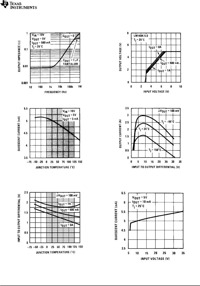
Output Impedance |
Dropout Characteristics |
Figure 13. |
Figure 14. |
Quiescent Current |
Peak Output Current |
Shaded area refers to LM340A/LM340-N, LM7805C, LM7812C and |
|
LM7815C. |
Figure 16. |
Figure 15. |
|
Dropout Voltage |
Quiescent Current |
Shaded area refers to LM340A/LM340-N, LM7805C, LM7812C and |
|
LM7815C. |
Figure 18. |
Figure 17. |
Copyright © 2000–2013, Texas Instruments Incorporated |
Submit Documentation Feedback |
9 |
Product Folder Links: LM340-N LM78xx
Loading...