


LF353DR
LF353
JFET-INPUT
DUAL OPERATIONAL AMPLIFIER
SLOS012B – MARCH 1987 – REVISED AUGUST 1994
1
POST OFFICE BOX 655303 • DALLAS, TEXAS 75265
D
Low Input Bias Current...50 pA Typ
D
Low Input Noise Current
0.01 pA/√Hz
Typ
D
Low Input Noise Voltage . . . 18 nV/√Hz Typ
D
Low Supply Current...3.6 mA Typ
D
High Input Impedance...10
12
Ω Typ
D
Internally Trimmed Offset Voltage
D
Gain Bandwidth...3 MHz Typ
D
High Slew Rate...13 V/µs Typ
description
This device is a low-cost, high-speed, JFET-input operational amplifier with very low input offset voltage. It
requires low supply current yet maintains a large gain-bandwidth product and a fast slew rate. In addition, the
matched high-voltage JFET input provides very low input bias and offset currents.
The LF353 can be used in applications such as high-speed integrators, digital-to-analog converters,
sample-and-hold circuits, and many other circuits.
The LF353 is characterized for operation from 0°C to 70°C.
symbol (each amplifier
+
–
IN –
OUT
IN +
AVAILABLE OPTIONS
PACKAGE
T
A
V
IO
max
AT 25°C
SMALL OUTLINE
(D)
PLASTIC DIP
(P)
0°C to 70°C 10 mV LF353D LF353P
The D packages are available taped and reeled. Add the suffix R to the
device type (ie., LF353DR).
absolute maximum ratings over operating free-air temperature range (unless otherwise noted)
Supply voltage, V
CC +
18 V. . . . . . . . . . . . . . . . . . . . . . . . . . . . . . . . . . . . . . . . . . . . . . . . . . . . . . . . . . . . . . . . . . . . . .
Supply voltage, V
CC –
–18 V. . . . . . . . . . . . . . . . . . . . . . . . . . . . . . . . . . . . . . . . . . . . . . . . . . . . . . . . . . . . . . . . . . . . .
Differential input voltage, V
ID
±30 V. . . . . . . . . . . . . . . . . . . . . . . . . . . . . . . . . . . . . . . . . . . . . . . . . . . . . . . . . . . . . . .
Input voltage, V
I
(see Note 1) ±15 V. . . . . . . . . . . . . . . . . . . . . . . . . . . . . . . . . . . . . . . . . . . . . . . . . . . . . . . . . . . . . .
Duration of output short circuit unlimited. . . . . . . . . . . . . . . . . . . . . . . . . . . . . . . . . . . . . . . . . . . . . . . . . . . . . . . . . . .
Continuous total power dissipation 500 mW. . . . . . . . . . . . . . . . . . . . . . . . . . . . . . . . . . . . . . . . . . . . . . . . . . . . . . .
Operating temperature range 0°C to 70°C. . . . . . . . . . . . . . . . . . . . . . . . . . . . . . . . . . . . . . . . . . . . . . . . . . . . . . . . .
Storage temperature range –65°C to 150°C. . . . . . . . . . . . . . . . . . . . . . . . . . . . . . . . . . . . . . . . . . . . . . . . . . . . . . . .
Lead temperature 1,6 mm (1/16 inch) from case for 10 seconds 260°C. . . . . . . . . . . . . . . . . . . . . . . . . . . . . . .
NOTE 1: Unless otherwise specified, the absolute maximum negative input voltage is equal to the negative power supply voltage.
Copyright 1994, Texas Instruments Incorporated
PRODUCTION DATA information is current as of publication date.
Products conform to specifications per the terms of Texas Instruments
standard warranty. Production processing does not necessarily include
testing of all parameters.
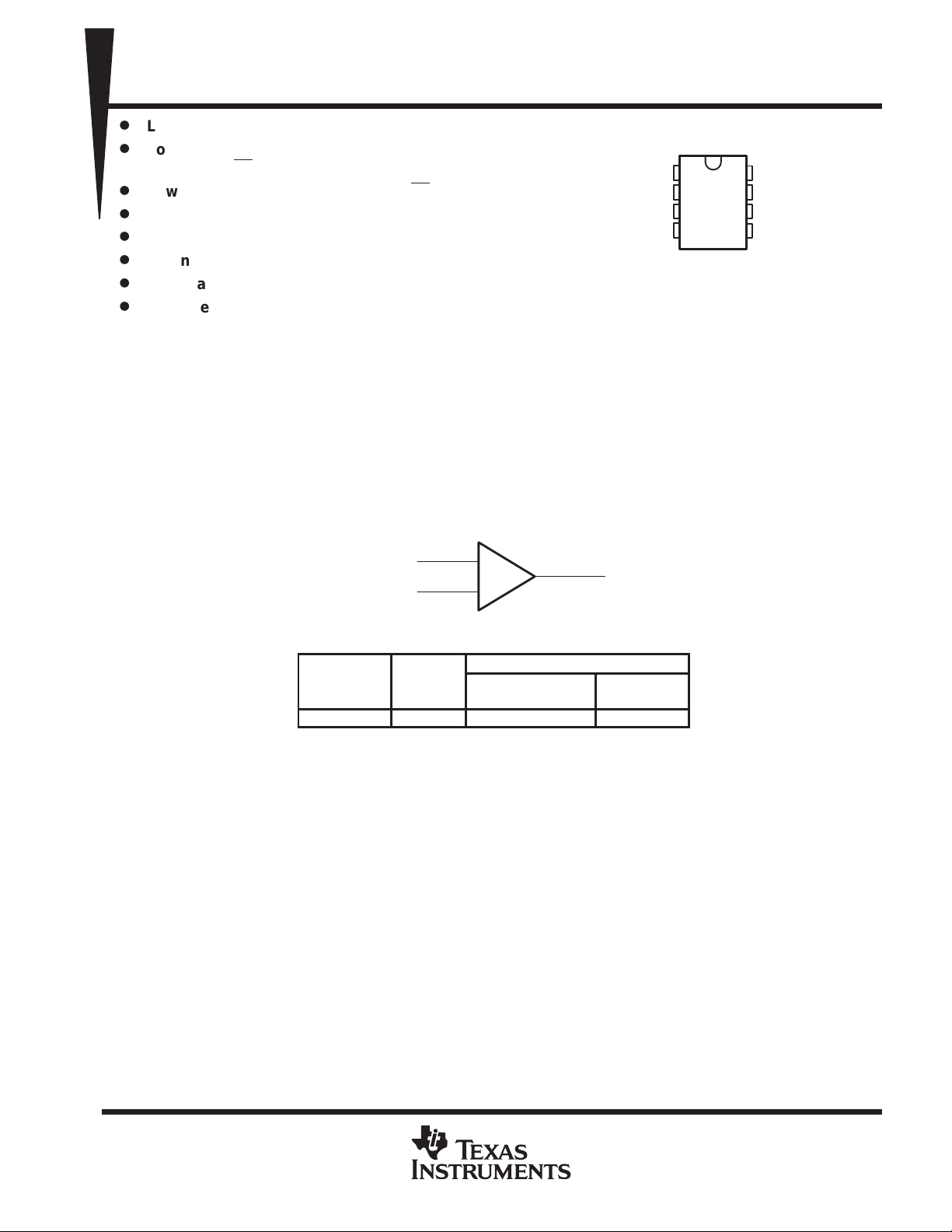
1
2
3
4
8
7
6
5
1OUT
1IN–
1IN+
V
CC–
V
CC+
2OUT
2IN–
2IN+
(TOP VIEW)
D OR P PACKAGE
 Loading...