


Texas Instruments LM311Y, LM311PWR, LM311PWLE, LM311PS, LM311P Datasheet
...LM111, LM211, LM311, LM311Y
DIFFERENTIAL COMPARATORS WITH STROBES
SLCS007A ± SEPTEMBER 1973 ± REVISED FEBRUARY 1992
D |
Fast Response Times |
LM111 . . . J PACKAGE |
||||
D |
Strobe Capability |
|
(TOP VIEW) |
|
||
D Maximum Input Bias Current . . . 300 nA |
NC |
|
|
|
NC |
|
1 |
14 |
|
||||
D Maximum Input Offset Current . . . 70 nA |
|
|||||
EMIT OUT |
2 |
13 |
|
NC |
||
D Can Operate From Single 5-V Supply |
IN+ |
3 |
12 |
|
NC |
|
D Designed to Be Interchangeable With |
IN± |
4 |
11 |
|
VCC + |
|
|
National Semiconductor LM111, LM211, |
NC |
5 |
10 |
|
NC |
|
and LM311 |
VCC ± |
6 |
9 |
|
COL OUT |
|
|
BALANCE |
7 |
8 |
|
BAL/STRB |
description
The LM111, LM211, and LM311 are single high-speed voltage comparators. These devices are designed to operate from a wide range of power supply voltages, including ± 15-V supplies for operational amplifiers and 5-V supplies for logic systems. The output levels are compatible with most TTL and MOS circuits. These comparators are capable of driving lamps or relays and switching voltages up to 50 V at 50 mA. All inputs and outputs can be isolated from system ground. The outputs can drive loads referenced to ground, VCC + or VCC ±. Offset balancing and strobe capabilities are available, and the outputs can be wire-OR connected. If the strobe is low, the output will be in the off state regardless of the differential input.
The LM111 is characterized for operation over the full military range of ±55°C to 125°C. The LM211 is characterized for operation from ±40°C to 85°C, and the LM311 is characterized for operation from 0°C to 70°C.
functional block diagram
BALANCE
BAL/STRB
IN+ |
+ |
COL OUT |
IN± |
± |
EMIT OUT |
|
|
LM111 . . . JG PACKAGE
LM211, LM311 . . . D, DB, P, OR PW PACKAGE
(TOP VIEW)
EMIT OUT |
1 |
8 |
|
VCC + |
|
IN+ |
2 |
7 |
|
COL OUT |
|
IN± |
3 |
6 |
|
BAL/STRB |
|
VCC ± |
4 |
5 |
|
BALANCE |
|
LM111 . . . U PACKAGE |
|||||
|
|
(TOP VIEW) |
|
||
EMIT OUT |
|
|
|
|
VCC + |
|
•1 |
10 |
|
||
|
|
||||
IN+ |
|
|
|||
|
2 |
9 |
|
COL OUT |
|
IN± |
|
3 |
8 |
|
NC |
NC |
|
4 |
7 |
|
BAL/STRB |
|
|
||||
VCC ± |
|
5 |
6 |
|
BALANCE |
|
|
||||
|
|
|
|
|
|
LM111 . . . FK PACKAGE
(TOP VIEW)
|
|
OUT |
|
+ |
|
|
|
NC |
EMIT |
NC |
CC |
NC |
|
|
V |
|
||||
NC |
3 |
2 |
1 |
20 19 |
NC |
|
4 |
|
|
|
18 |
||
IN+ |
5 |
|
|
|
17 |
COL OUT |
NC |
6 |
|
|
|
16 |
NC |
IN± |
7 |
|
|
|
15 |
BAL/STRB |
NC |
8 |
|
|
|
14 |
NC |
|
9 |
10 11 12 13 |
|
|||
|
NC |
CC± |
NC |
BALANCE |
NC |
|
|
V |
|
||||
PRODUCTION DATA information is current as of publication date. Products conform to specifications per the terms of Texas Instruments standard warranty. Production processing does not necessarily include testing of all parameters.
Copyright 1992, Texas Instruments Incorporated
POST OFFICE BOX 655303 •DALLAS, TEXAS 75265 |
1 |
LM111, LM211, LM311, LM311Y
DIFFERENTIAL COMPARATORS WITH STROBES
SLCS007A ± SEPTEMBER 1973 ± REVISED FEBRUARY 1992
AVAILABLE OPTIONS
|
|
|
|
|
PACKAGED DEVICES |
|
|
|
CHIP |
||
|
VIOmax |
SMALL |
|
CHIP |
CERAMIC |
CERAMIC |
PLASTIC |
|
|
||
TA |
SSOP |
TSSOP |
FLATPACK |
FORM |
|||||||
at 25°C |
OUTLINE |
CARRIER |
DIP |
DIP |
DIP |
||||||
|
(DB) |
(PW) |
(U) |
(Y) |
|||||||
|
|
(D)² |
(FK) |
(J) |
(JG) |
(P) |
|||||
|
|
|
|
|
|
||||||
0°C |
|
|
|
|
|
|
|
|
|
|
|
to |
7.5 mV |
LM311D LM311DBLE |
|
|
|
LM311P LM311PWLE |
|
LM311Y |
|||
70°C |
|
|
|
|
|
|
|
|
|
|
|
|
|
|
|
|
|
|
|
|
|
|
|
± 40°C |
|
|
|
|
|
|
|
|
|
|
|
to |
3 mV |
LM211D |
|
|
|
|
LM211P |
|
|
|
|
85°C |
|
|
|
|
|
|
|
|
|
|
|
|
|
|
|
|
|
|
|
|
|
|
|
± 55°C |
|
|
|
|
|
|
|
|
|
|
|
to |
3 mV |
|
|
LM111FK |
LM111J |
LM111JG |
|
|
LM111U |
|
|
125°C |
|
|
|
|
|
|
|
² The D package is available taped and reeled. Add the suffix R (e.g., LM311DR). The DB and PW packages are only available left-end taped and |
|||||||
reeled. |
|
|
|
|
|
|
|
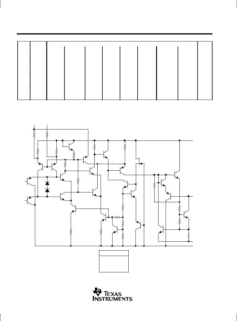
schematic |
|
|
|
|
|
|
|
BAL/STRB |
BALANCE |
|
|
|
|
|
|
|
|
|
|
|
|
|
|
300 Ω |
300 Ω |
|
|
|
|
|
|
|
|
|
|
|
|
|
VCC + |
1.3 |
1.3 |
|
|
750 Ω |
600 Ω |
|
|
|
|
|
|
|
|
||
kΩ |
kΩ |
70 |
Ω |
|
|
|
|
|
|
|
|
|
|
||
|
|
1.2 kΩ |
|
|
|
|
|
IN + |
|
|
1.2 kΩ |
|
|
|
|
|
|
|
|
|
|
4 kΩ |
|
|
|
|
|
|
|
|
COL OUT |
IN ± |
|
|
|
|
|
|
|
|
|
|
|
|
400 Ω |
130 |
Ω |
|
|
|
|
|
|
||
|
|
|
|
|
60 Ω |
|
|
|
|
|
|
|
450 Ω |
600 Ω |
|
|
|
|
|
|
|
|
|
|
|
250 Ω |
200 Ω |
|
|
|
|
|
|
|
|
|
2 kΩ |
|
4 Ω |
|
|
|
|
|
|
|
EMIT OUT |
|
|
|
|
|
|
|
VCC ± |
Component Count
Resistors 20
Diodes 2
Epifet 1
All resistor values shown are nominal. |
Transistors |
22 |
|
|
|
|
|
|
|
|
|
2 |
POST OFFICE BOX 655303 •DALLAS, TEXAS 75265 |

LM111, LM211, LM311, LM311Y
DIFFERENTIAL COMPARATORS WITH STROBES
SLCS007A ± SEPTEMBER 1973 ± REVISED FEBRUARY 1992
LM311Y chip information
This chip, when properly assembled, displays characteristics similar to the LM311. Thermal compression or ultrasonic bonding may be used on the doped-aluminum bonding pads. Chips may be mounted with conductive epoxy or a gold-silicon preform.
BONDING PAD ASSIGNMENTS
(1) |
(8) |
(7)
(2)
62
(3)
(4)
(5) (6)
50
|
|
|
|
|
COL |
|
|
|
VCC+ |
OUT |
|
(5) |
|
|
|||
(8) |
(7) |
||||
BALANCE |
|
|
|
|
|
|
|
|
|
|
|
(2) |
|
|
|
|
|
IN+ |
+ |
|
|
|
|
(3) |
± |
|
|
|
|
IN± |
|
|
|
||
|
|
|
|||
(6) |
|
|
|
|
|
BAL/STRB |
|
|
|
(4) |
(1) |
|
|
|
|||
|
|
|
|
||
|
|
|
|
|
|
|
|
|
VCC ± |
EMIT |
|
|
|
|
|
|
OUT |
CHIP THICKNESS: 15 TYPICAL BONDING PADS: 4 × 4 MINIMUM TJ max = 150°C
TOLERANCES ARE ± 10%.
ALL DIMENSIONS ARE IN MILS.
POST OFFICE BOX 655303 •DALLAS, TEXAS 75265 |
3 |
LM111, LM211, LM311, LM311Y
DIFFERENTIAL COMPARATORS WITH STROBES
SLCS007A ± SEPTEMBER 1973 ± REVISED FEBRUARY 1992
absolute maximum ratings over operating free-air temperature range (unless otherwise noted)²
Supply voltage, VCC+ (see Note 1) . . . . |
. . . . . . . . . . . . . . . . . . . . . . . . . . . . . . . . . . . . . . . . . . . . . |
. . . . . . . . . . 18 V |
Supply voltage, VCC± (see Note 1) . . . . |
. . . . . . . . . . . . . . . . . . . . . . . . . . . . . . . . . . . . . . . . . . . . . . |
. . . . . . . . ±18 V |
Supply voltage, VCC+ ± VCC± . . . . . . . . |
. . . . . . . . . . . . . . . . . . . . . . . . . . . . . . . . . . . . . . . . . . . . . . |
. . . . . . . . . 36 V |
Differential input voltage, VID (see Note 2) . . . . . . . . . . . . . . . . . . . . . . . . . . . . . . . . . . . . . . . . . . . |
. . . . . . . . ± 30 V |
|
Input voltage, VI (either input, see Notes 1 and 3) . . . . . . . . . . . . . . . . . . . . . . . . . . . . . . . . . . . . |
. . . . . . . . ± 15 V |
|
Voltage from emitter output to VCC ± . . . |
. . . . . . . . . . . . . . . . . . . . . . . . . . . . . . . . . . . . . . . . . . . . . . |
. . . . . . . . . 30 V |
Voltage from collector output to VCC ± : |
LM111 . . . . . . . . . . . . . . . . . . . . . . . . . . . . . . . . . . . . . . . |
. . . . . . . . . 50 V |
|
LM211 . . . . . . . . . . . . . . . . . . . . . . . . . . . . . . . . . . . . . . . |
. . . . . . . . . 50 V |
|
LM311 . . . . . . . . . . . . . . . . . . . . . . . . . . . . . . . . . . . . . . . |
. . . . . . . . . 40 V |
Duration of output short circuit (see Note 4) . . . . . . . . . . . . . . . . . . . . . . . . . . . . . . . . . . . . . . . . . . |
. . . . . . . . . 10 s |
|
Continuous total dissipation . . . . . . . . . . |
. . . . . . . . . . . . . . . . . . . . . . . . . . . . . . . . . See Dissipation Rating Table |
|
Operating free-air temperature range, TA: LM111 . . . . . . . . . . . . . . . . . . . . . . . . . . . . . . . . . . . . . |
±55°C to 125°C |
|
|
LM211 . . . . . . . . . . . . . . . . . . . . . . . . . . . . . . . . . . . . . . |
±40°C to 85°C |
|
LM311 . . . . . . . . . . . . . . . . . . . . . . . . . . . . . . . . . . . . . . |
. . 0°C to 70°C |
Storage temperature range . . . . . . . . . . . |
. . . . . . . . . . . . . . . . . . . . . . . . . . . . . . . . . . . . . . . . . . . . . |
±65°C to 150°C |
Case temperature for 60 seconds: FK package . . . . . . . . . . . . . . . . . . . . . . . . . . . . . . . . . . . . . . . |
. . . . . . . 260°C |
|
Lead temperature 1,6 mm (1/16 inch) from case for 10 seconds: J, JG, or U package . . . . . . |
. . . . . . . 300°C |
|
Lead temperature 1,6 mm (1/16 inch) from case for 60 seconds: D, DB, P, or PW package . |
. . . . . . . 260°C |
|
² Stresses beyond those listed under ªabsolute maximum ratingsº may cause permanent damage to the device. These are stress ratings only, and functional operation of the device at these or any other conditions beyond those indicated under ªrecommended operating conditionsº is not
implied. Exposure to absolute-maximum-rated conditions for extended periods may affect device reliability. |
|
||||||
NOTES: 1. All voltage values, unless otherwise noted, are with respect to the midpoint between VCC+ and VCC±. |
|
||||||
2. Differential voltages are at IN+ with respect to IN ±. |
|
|
|
||||
3. |
The magnitude of the input voltage must never exceed the magnitude of the supply voltage or ± 15 V, whichever is less. |
||||||
4. The output may be shorted to ground or either power supply. |
|
|
|
||||
|
|
|
DISSIPATION RATING TABLE |
|
|
||
|
|
|
|
|
|
|
|
PACKAGE |
TA ≤ 25°C |
DERATING |
DERATE |
TA = 70°C |
TA = 85°C |
TA = 125°C |
|
POWER RATING |
FACTOR |
ABOVE TA |
POWER RATING |
POWER RATING |
POWER RATING |
||
|
|||||||
D |
500 mW |
5.8 mW/°C |
64°C |
464 mW |
377 mW |
± |
|
DB or PW |
500 mW |
4.2 mW/°C |
31°C |
336 mW |
± |
± |
|
FK |
500 mW |
11.0 mW/°C |
105°C |
500 mW |
500 mW |
275 mW |
|
J |
500 mW |
11.0 mW/°C |
105°C |
500 mW |
500 mW |
275 mW |
|
JG |
500 mW |
8.4 mW/°C |
90°C |
500 mW |
500 mW |
210 mW |
|
P |
500 mW |
8.0 mW/°C |
88°C |
500 mW |
500 mW |
± |
|
U |
500 mW |
5.4 mW/°C |
57°C |
432 mW |
351 mW |
135 mW |
|
recommended operating conditions
|
|
MIN |
MAX |
UNIT |
|
|
|
|
|
Supply voltage, VCC + ± VCC ± |
|
3.5 |
30 |
V |
Input voltage ( | VCC± | ≤ 15 V) |
|
VCC± + 0.5 |
VCC+ ±1.5 |
V |
|
LM111 |
± 55 |
125 |
|
Operating free-air temperature range, TA |
|
|
|
°C |
LM211 |
± 40 |
85 |
||
|
LM311 |
0 |
70 |
|
4 |
POST OFFICE BOX 655303 •DALLAS, TEXAS 75265 |
LM111, LM211, LM311, LM311Y
DIFFERENTIAL COMPARATORS WITH STROBES
SLCS007A ± SEPTEMBER 1973 ± REVISED FEBRUARY 1992
electrical characteristics at specified free-air temperature, VCC ± = ±15 V (unless otherwise noted)
|
PARAMETER |
TEST CONDITIONS |
T ² |
LM111, LM211 |
|
LM311 |
|
UNIT |
|||
|
|
|
|
|
|
|
|||||
|
MIN |
TYP³ |
MAX |
MIN |
TYP³ |
MAX |
|||||
|
|
|
|
A |
|
||||||
VIO |
Input offset voltage |
See Note 5 |
|
25°C |
|
0.7 |
3 |
|
2 |
7.5 |
mV |
|
|
|
|
|
|
|
|
||||
|
Full range |
|
|
4 |
|
|
10 |
||||
|
|
|
|
|
|
|
|
|
|||
|
|
|
|
|
|
|
|
|
|
|
|
IIO |
Input offset current |
See Note 5 |
|
25°C |
|
4 |
10 |
|
6 |
50 |
nA |
|
|
|
|
|
|
|
|
||||
|
Full range |
|
|
20 |
|
|
70 |
||||
|
|
|
|
|
|
|
|
|
|||
|
|
|
|
|
|
|
|
|
|
|
|
IIB |
Input bias current |
VO = 1 V to 14 V |
|
25°C |
|
75 |
100 |
|
100 |
250 |
nA |
|
|
|
|
|
|
|
|
||||
|
Full range |
|
|
150 |
|
|
300 |
||||
|
|
|
|
|
|
|
|
|
|||
|
|
|
|
|
|
|
|
|
|
|
|
IIL(S) |
Low-level strobe |
V(strobe) = 0.3 V, |
VID ≤ ± 10 mV |
25°C |
|
± 3 |
|
|
± 3 |
|
mA |
current (see Note 6) |
|
|
|
|
|||||||
|
|
|
|
|
|
|
|
|
|
|
|
|
|
|
|
|
|
|
|
|
|
|
|
|
Common-mode |
|
|
|
13 |
13.8 |
|
13 |
13.8 |
|
|
VICR |
|
|
Full range |
to |
to |
|
to |
to |
|
V |
|
input voltage range |
|
|
|
|
|||||||
|
|
|
|
± 14.5 |
± 14.7 |
|
± 14.5 |
± 14.7 |
|
|
|
|
|
|
|
|
|
|
|
||||
|
|
|
|
|
|
|
|
|
|
|
|
|
Large-signal |
|
|
|
|
|
|
|
|
|
|
AVD |
differential voltage |
VO = 5 V to 35 V, |
RL = 1 kΩ |
25°C |
40 |
200 |
|
40 |
200 |
|
V/mV |
|
amplification |
|
|
|
|
|
|
|
|
|
|
|
|
|
|
|
|
|
|
|
|
|
|
|
High-level (collector) |
I(strobe) = ±3 mA, |
|
25°C |
|
0.2 |
10 |
|
|
|
nA |
IOH |
VID = 5 mV, |
VOH = 35 V |
Full range |
|
|
0.5 |
|
|
|
μA |
|
output current |
|
|
|
|
|
||||||
|
VID = 5 mV, |
VOH = 35 V |
25°C |
|
|
|
|
0.2 |
50 |
nA |
|
|
|
|
|
|
|
||||||
|
|
IOL = 50 mA |
VID = ± 5 mV |
25°C |
|
0.75 |
1.5 |
|
|
|
|
|
Low-level |
VID = ± 10 mV |
25°C |
|
|
|
|
0.75 |
1.5 |
|
|
|
|
|
|
|
|
|
|||||
VOL |
(collector-to-emitter) |
VCC+ = 4.5 V, |
V = ± 6 mV |
Full range |
|
0.23 |
0.4 |
|
|
|
V |
|
output voltage |
VCC± = 0, |
ID |
|
|
|
|
|
|
|
|
|
|
VID = ± 10 mV |
Full range |
|
|
|
|
0.23 |
0.4 |
|
|
|
|
IOL = 8 mA |
|
|
|
|
|
||||
ICC + |
Supply current from |
VID = ± 10 mV, |
No load |
25°C |
|
5.1 |
6 |
|
5.1 |
7.5 |
mA |
VCC +, output low |
|
|
|||||||||
|
|
|
|
|
|
|
|
|
|
|
|
ICC ± |
Supply current from |
VID = 10 mV, |
No load |
25°C |
|
± 4.1 |
± 5 |
|
± 4.1 |
± 5 |
mA |
VCC ±, output high |
|
|
|||||||||
|
|
|
|
|
|
|
|
|
|
|
|
² Unless otherwise noted, all characteristics are measured with BALANCE and BAL/STRB open and the emitter output grounded. Full range for LM111 is ± 55°C to 125°C, for LM211 is ± 40°C to 85°C, and for LM311 is 0°C to 70°C.
³ All typical values are at TA = 25°C.
NOTES: 5. The offset voltages and offset currents given are the maximum values required to drive the collector output up to 14 V or down to 1 V with a pullup resistor of 7.5 kΩ to VCC +. These parameters actually define an error band and take into account the worst-case effects of voltage gain and input impedance.
6. The strobe should not be shorted to ground; it should be current driven at ± 3 mA to ± 5 mA (see Figures 13 and 27).
switching characteristics, VCC ± = ±15 V, |
TA = 25°C |
|
|
|
|
|
PARAMETER |
|
TEST CONDITIONS |
|
LM111, LM211, LM311 |
UNIT |
|
|
|
|
|
|||
|
|
MIN TYP |
MAX |
|||
|
|
|
|
|
||
|
|
|
|
|
|
|
Response time, low-to-high-level output |
RC = 500 Ω to 5 V, CL = 5 pF, |
See Note 7 |
115 |
|
ns |
|
|
|
|
|
|||
Response time, high-to-low-level output |
165 |
|
ns |
|||
|
|
|
|
|||
|
|
|
|
|
|
|
NOTE 7: The response time specified is for a 100-mV input step with 5-mV overdrive and is the interval between the input step function and the instant when the output crosses 1.4 V.
POST OFFICE BOX 655303 •DALLAS, TEXAS 75265 |
5 |
 Loading...