


 Loading...
PRODUCT |
Sample & |
TECHNICAL |
TOOLS & |
Support & |
FOLDER |
Buy |
DOCUMENTS |
SOFTWARE |
Community |
LMK04803, LMK04805, LMK04806, LMK04808
SNAS489K –MARCH 2011–REVISED DECEMBER 2014
LMK0480x Low-Noise Clock Jitter Cleaner with Dual Loop PLLs
1 Features
•Ultra-Low RMS Jitter Performance
–111 fs RMS Jitter (12 kHz to 20 MHz)
–123 fs RMS Jitter (100 Hz to 20 MHz)
•Dual Loop PLLatinum™ PLL Architecture
•PLL1
–Integrated Low-Noise Crystal Oscillator Circuit
–Holdover Mode when Input Clocks are Lost
–Automatic or Manual Triggering/Recovery
•PLL2
–Normalized PLL Noise Floor of –227 dBc/Hz
–Phase Detector Rate up to 155 MHz
–OSCin Frequency-Doubler
–Integrated Low-Noise VCO
•2 Redundant Input Clocks with LOS
–Automatic and Manual Switch-Over Modes
•50 % Duty Cycle Output Divides, 1 to 1045 (Even and Odd)
•12 LVPECL, LVDS, or LVCMOS Programmable Outputs
•Digital Delay: Fixed or Dynamically Adjustable
•25 ps Step Analog Delay Control.
•14 Differential Outputs. Up to 26 Single Ended.
–Up to 6 VCXO/Crystal Buffered Outputs
•Clock Rates of up to 1536 MHz
•0-Delay Mode
•Three Default Clock Outputs at Power Up
•Multi-Mode: Dual PLL, Single PLL, and Clock Distribution
•Industrial Temperature Range: –40 to 85°C
•3.15-V to 3.45-V Operation
•2 Dedicated Buffered/Divided OSCin Clocks
•Package: 64-Pin WQFN (9.0 × 9.0 × 0.8 mm)
2 Applications
•Data Converter Clocking
•Wireless Infrastructure
•Networking, SONET/SDH, DSLAM
•Medical / Video / Military / Aerospace
•Test and Measurement
3 Description
The LMK0480x family is the industry's highest performance clock conditioner with superior clock jitter cleaning, generation, and distribution with advanced features to meet next generation system requirements. The dual loop PLLatinum™ architecture is capable of 111 fs rms jitter (12 kHz to 20 MHz) using a low noise VCXO module or sub-200 fs rms jitter (12 kHz to 20 MHz) using a low cost external crystal and varactor diode.
The dual loop architecture consists of two highperformance phase-locked loops (PLL), a low-noise crystal oscillator circuit, and a high-performance voltage controlled oscillator (VCO). The first PLL (PLL1) provides low-noise jitter cleaner functionality while the second PLL (PLL2) performs the clock generation. PLL1 can be configured to either work with an external VCXO module or the integrated crystal oscillator with an external tunable crystal and varactor diode. When paired with a very narrow loop bandwidth, PLL1 uses the superior close-in phase noise (offsets below 50 kHz) of the VCXO module or the tunable crystal to clean the input clock. The output of PLL1 is used as the clean input reference to PLL2 where it locks the integrated VCO. The loop bandwidth of PLL2 can be optimized to clean the farout phase noise (offsets above 50 kHz) where the integrated VCO outperforms the VCXO module or tunable crystal used in PLL1.
|
Device Information |
|
|
PART NUMBER |
VCO FREQUENCY |
REFERENCE |
|
INPUTS |
|||
|
|
||
LMK04803 |
1840 to 2030 MHz |
|
|
LMK04805 |
2148 to 2370 MHz |
2 |
|
LMK04806 |
2370 to 2600 MHz |
||
|
|||
LMK04808 |
2750 to 3072 MHz |
|
(1)For all available packages, see the orderable addendum at the end of the datasheet.
|
Simplified Schematic |
|
|||
|
Crystal or |
OSCout0/ |
|
0XOWLSOH ³FOHDQ´ |
|
|
OSCout1 |
LMX2541 |
|||
|
clocks at different |
||||
Recovered |
VCXO |
|
|
||
|
|
PLL+VCO |
frequencies |
||
³GLUW\´ FORFN RU |
|
|
|
||
|
|
|
|
||
clean clock |
CLKin0 |
|
CLKout0, 1 |
|
|
Backup |
|
LMK0480x |
CLKout2 |
FPGA |
|
Reference |
|
|
|
Serializer/ |
|
Clock |
CLKin1 |
Precision Clock |
CLKout3 |
FPGA |
|
|
|
|
|
Deserializer |
|
|
|
Conditioner |
|
|
|
|
|
CLKout4, 5, 6, 7 |
|
|
|
|
I |
|
|
|
|
|
|
|
|
|
|
|
CLKout11 |
|
CLKout8A |
|
|
IF |
|
|
|
|
|
CLKout9 |
|
|
|
DAC |
|
|
|
|
ADC |
||
|
|
CPLD |
DAC |
||
|
Q |
|
|
||
|
|
|
|
|
|
An IMPORTANT NOTICE at the end of this data sheet addresses availability, warranty, changes, use in safety-critical applications, intellectual property matters and other important disclaimers. PRODUCTION DATA.

LMK04803, LMK04805, LMK04806, LMK04808
SNAS489K –MARCH 2011 –REVISED DECEMBER 2014 www.ti.com
Table of Contents
1 |
Features .................................................................. |
1 |
|
8.5 |
Programming........................................................... |
47 |
|
2 |
Applications ........................................................... |
1 |
|
8.6 |
Register Maps ......................................................... |
51 |
|
3 |
Description ............................................................. |
1 |
9 |
Application and Implementation ........................ |
97 |
||
4 |
Revision History..................................................... |
2 |
|
9.1 |
Application Information............................................ |
97 |
|
5 |
Pin Configuration and Functions |
4 |
|
9.2 |
Typical Applications .............................................. |
114 |
|
|
9.3 |
System Examples |
122 |
||||
6 |
Specifications |
6 |
|
||||
|
9.4 |
Do's and Don'ts |
124 |
||||
|
6.1 |
Absolute Maximum Ratings |
6 |
|
|||
|
10 |
Power Supply Recommendations |
125 |
||||
|
6.2 |
ESD Ratings |
6 |
||||
|
|
10.1 |
Pin Connection Recommendations |
125 |
|||
|
6.3 |
Recommended Operating Conditions |
6 |
|
|||
|
|
10.2 Current Consumption and Power Dissipation |
|
||||
|
6.4 |
Thermal Information |
7 |
|
|
||
|
|
|
Calculations |
126 |
|||
|
6.5 |
Electrical Characteristics |
7 |
|
|
||
|
11 |
Layout |
129 |
||||
|
6.6 |
Timing Requirements |
13 |
||||
|
|
11.1 |
Layout Guidelines |
129 |
|||
|
6.7 |
Typical Characteristics: Clock Output AC |
|
|
|||
|
|
|
11.2 |
Layout Example |
130 |
||
|
|
Characteristics |
14 |
|
|||
|
|
12 |
Device and Documentation Support |
131 |
|||
7 |
Parameter Measurement Information ................ |
15 |
|||||
|
7.1 |
Charge Pump Current Specification Definitions |
15 |
|
12.1 |
Device Support.................................................... |
131 |
|
|
12.2 |
Documentation Support |
131 |
|||
|
7.2 |
Differential Voltage Measurement Terminology |
16 |
|
|||
|
|
12.3 |
Related Links |
131 |
|||
8 |
Detailed Description |
17 |
|
||||
|
12.4 |
Trademarks |
131 |
||||
|
8.1 |
Overview |
17 |
|
|||
|
|
12.5 |
Electrostatic Discharge Caution |
131 |
|||
|
8.2 |
Functional Block Diagram |
21 |
|
|||
|
|
12.6 |
Glossary |
131 |
|||
|
8.3 |
Feature Description |
22 |
|
|||
|
13 |
Mechanical, Packaging, and Orderable |
|
||||
|
8.4 |
Device Functional Modes........................................ |
43 |
131 |
|||
|
|
|
|
|
Information ......................................................... |
||
|
|
|
|
|
|
|
|
4 Revision History
Changes from Revision J (March 2013) to Revision K |
Page |
• Changed 90 to 80 and 80 to 90 for fCLKout-startup parameter in Electrical Characteristics |
....................................................... 11 |
•Added "Specification is not valid for CLKoutX or CLKoutY in analog delay mode" in table note for Electrical
Characteristics ..................................................................................................................................................................... |
11 |
•Changed "Temperature" to "Ambient Temperature" in heading titled "Charge Pump Output Current Magnitude
Variation vs. Ambient Temperature" .................................................................................................................................... |
15 |
• Added "temporarily" in VCXO/CRYSTAL Buffered Outputs ................................................................................................ |
18 |
• Changed from "n possible" to "D possible" in 0-Delay ......................................................................................................... |
20 |
• Changed "can" to "cannot" in Input Clock Switching - Pin Select Mode .............................................................................. |
24 |
• Deleted Clock Switch Event without Holdover in Clock Switch Event with Holdover .......................................................... |
25 |
• Added paragraph beginning "For applications ..." in PLL2 Frequency Doubler ................................................................... |
29 |
• Changed 5 to15 in Table 11 ................................................................................................................................................. |
42 |
• Deleted Mode 5 row in Table 12 .......................................................................................................................................... |
43 |
• Added Mode 15 Additional Configurations section .............................................................................................................. |
46 |
•In Table 16, added [27:26], [23:22], and [21:20] for Register 27 row. Added [31:20] for R28. Added [26:24] for R30.
Added [7:6]. .......................................................................................................................................................................... |
51 |
•In Table 18, changed "Actual PLL2 N divider value used in calibration routine". Added footnote "Inversion for Status
0 and 1 pins is only valid for CLKin_SELECT_MODE = 0x06"............................................................................................ |
56 |
• In Table 28, added "to reduce supply..." footnote for 9 through 14. Added footnote "To reduce supply switching and |
|
crosstalk noise, it is recommended to use a complementary LVCMOS output type such as 6 or 7". ................................. |
64 |
• Added footnote "To reduce supply" for 8 through 14 in Table 32 ....................................................................................... |
66 |
• Changed "Divide" to "Definition" in Table 39, Table 40, Table 61, and Table 62 ................................................................ |
68 |
• Changed to "MUX OUTPUT" in Table header row in Table 42............................................................................................ |
69 |
•In Table 43, added footnote, "Contact TI Applications for more information on using this mode". Changed to "Dual
2 |
Submit Documentation Feedback |
Copyright © 2011–2014, Texas Instruments Incorporated |
Product Folder Links: LMK04803 LMK04805 LMK04806 LMK04808

|
LMK04803, LMK04805, LMK04806, LMK04808 |
|
www.ti.com |
SNAS489K –MARCH 2011–REVISED DECEMBER 2014 |
|
Revision History (continued) |
|
|
PLL, External VCO (Fin), 0-Delay" for 15 (0x0F) |
................................................................................................................. |
70 |
• Added "Inversion for Status 0 and 1 pins is only valid for CLKin_SELECT_MODE = 0x06" in CLKin_Sel_INV ................. |
78 |
|
•In FORCE_HOLDOVER, added "(EN_TRACK = 0 or 1, EN_MAN_DAC =1)". Added "(EN_TRACK = 1,
EN_MAN_DAC = 0, EN_VTUNE_RAIL_DET = 0)".............................................................................................................. |
82 |
• Changed to R[23:14] in DAC_CNT....................................................................................................................................... |
83 |
• In Table 90, added (0x0000), (0x0001), (0x0002), (0x0003). Changed "Divide" to "Value" in the header row. .................. |
87 |
• Added (0x00) through (0x04) in Table 91............................................................................................................................. |
88 |
• Added PLL2 Frequency Doubler .......................................................................................................................................... |
88 |
• Changed from "Divide" to "Value" in Table 95 ..................................................................................................................... |
89 |
• Added PLL2 Frequency Doubler reference in Table 103..................................................................................................... |
92 |
• Added note "Unless in 0-delay..." in PLL2_N_CAL, PLL2 N Calibration Divider ................................................................ |
93 |
• Changed "Mode_MUX1" to "VCO_MUX" in PLL2_P, PLL2 N Prescaler Divider................................................................. |
94 |
• Changed "register" to "Defintion" in table header row for Table 110 ................................................................................... |
95 |
• Updated Minimum Digital Lock Detect Time Calculation Example ................................................................................... |
107 |
•Added "Performance of other LMK0480x devices will be similar" in Optional Crystal Oscillator Implementation
(OSCin/OSCin*).................................................................................................................................................................. |
110 |
• Changed to "(fs rms)" in Table 125 ................................................................................................................................... |
111 |
• Added text in red for Figure 40 .......................................................................................................................................... |
123 |
• In Vcc2, Vcc3, Vcc10, Vcc11, Vcc12, Vcc13 (CLKout Vccs), added bullet point starting with "It is recommended... |
" |
Changed ≤ 10 MHz to ≤ 30 MHz ........................................................................................................................................ |
125 |
• Added paragraph "It is recommended..." in Vcc5 (CLKin and OSCout1), Vcc7 (OSCin and OSCout0) ........................... |
126 |
• Added Mode = 15. Removed Mode = 5 in Table 127 ........................................................................................................ |
127 |
• Deleted "of about 2 square inches" in Layout Guidelines .................................................................................................. |
129 |
Changes from Revision I (March 2013) to Revision J |
Page |
• Changed layout of National Data Sheet to TI format ............................................................................................................. |
1 |
Copyright © 2011–2014, Texas Instruments Incorporated |
Submit Documentation Feedback |
3 |
Product Folder Links: LMK04803 LMK04805 LMK04806 LMK04808
LMK04803, LMK04805, LMK04806, LMK04808
SNAS489K –MARCH 2011 –REVISED DECEMBER 2014 |
www.ti.com |
5 Pin Configuration and Functions
64-Pin WQFN with Exposed Pad NKD Package
(Top View)
|
<![if ! IE]> <![endif]>Vcc13 |
<![if ! IE]> <![endif]>Status CLKin1 |
<![if ! IE]> <![endif]>Status CLKin0 |
<![if ! IE]> <![endif]>CLKout11 |
<![if ! IE]> <![endif]>CLKout11* |
<![if ! IE]> <![endif]>CLKout10* |
<![if ! IE]> <![endif]>CLKout10 |
<![if ! IE]> <![endif]>Vcc12 |
<![if ! IE]> <![endif]>CLKout9 |
<![if ! IE]> <![endif]>CLKout9* |
<![if ! IE]> <![endif]>CLKout8* |
<![if ! IE]> <![endif]>CLKout8 |
<![if ! IE]> <![endif]>Vcc11 |
<![if ! IE]> <![endif]>CLKout7 |
<![if ! IE]> <![endif]>CLKout7* |
<![if ! IE]> <![endif]>CLKout6* |
|
|
64 |
63 |
62 |
61 |
60 |
59 |
58 |
57 |
56 |
55 |
54 |
53 |
52 |
51 |
50 |
49 |
|
CLKout0 |
1 |
|
|
|
|
|
|
|
|
|
|
|
|
|
|
48 |
CLKout6 |
|
|
|
|
|
|
|
|
|
|
|
|
|
|
|
|
||
CLKout0* |
2 |
|
|
|
|
|
|
|
|
|
|
|
|
|
|
47 |
Vcc10 |
|
|
|
|
|
|
|
|
|
|
|
|
|
|
|
|
||
CLKout1* |
3 |
|
|
|
|
|
|
|
|
|
|
|
|
|
|
46 |
DATAuWire |
|
|
|
|
|
|
|
|
|
|
|
|
|
|
|
|
||
CLKout1 |
4 |
|
|
|
|
|
|
|
|
|
|
|
|
|
|
45 |
CLKuWire |
|
|
|
|
|
|
|
|
|
|
|
|
|
|
|
|
||
NC |
5 |
|
|
|
|
|
|
|
|
|
|
|
|
|
|
44 |
LEuWire |
|
|
|
|
|
|
|
|
|
|
|
|
|
|
|
|
||
SYNC |
6 |
|
|
|
|
|
|
|
|
|
|
|
|
|
|
43 |
Vcc9 |
|
|
|
|
|
|
|
|
|
|
|
|
|
|
|
|
||
NC |
7 |
|
|
|
|
|
|
|
|
|
|
|
|
|
|
42 |
CPout2 |
|
|
|
|
|
|
|
|
|
|
|
|
|
|
|
|
||
NC |
8 |
|
|
|
|
|
|
|
|
|
|
|
|
|
|
41 |
Vcc8 |
|
|
|
|
|
|
|
|
|
|
|
|
|
|
|
|
||
NC |
9 |
|
|
|
|
|
TOP DOWN VIEW |
|
|
|
|
40 |
OSCout0* |
||||
|
|
|
|
|
|
|
|
|
|
|
|
|
|
||||
|
|
|
|
|
|
|
|
|
|
|
|
|
|
|
|
||
Vcc1 |
10 |
|
|
|
|
|
|
|
|
|
|
|
|
|
|
39 |
OSCout0 |
|
|
|
|
|
|
|
|
|
|
|
|
|
|
|
|
||
LDObyp1 |
11 |
|
|
|
|
|
|
|
|
|
|
|
|
|
|
38 |
Vcc7 |
|
|
|
|
|
|
|
|
|
|
|
|
|
|
|
|
||
LDObyp2 |
12 |
|
|
|
|
|
|
|
|
|
|
|
|
|
|
37 |
OSCin* |
|
|
|
|
|
|
|
|
|
|
|
|
|
|
|
|
||
CLKout2 |
13 |
|
|
|
|
|
|
|
|
|
|
|
|
|
|
36 |
OSCin |
|
|
|
|
|
|
|
|
|
|
|
|
|
|
|
|
||
CLKout2* |
14 |
|
|
|
|
|
|
|
|
|
|
|
|
|
|
35 |
Vcc6 |
|
|
|
|
|
|
|
|
|
|
|
|
|
|
|
|
||
CLKout3* |
15 |
DAP |
|
|
|
|
|
|
|
|
|
|
|
|
34 |
CPout1 |
|
CLKout3 |
16 |
|
|
|
|
|
|
|
|
|
|
|
|
|
|
33 |
Status_LD |
|
|
|
|
|
|
|
|
|
|
|
|
|
|
|
|
||
|
17 |
18 |
19 |
20 |
21 |
22 |
23 |
24 |
25 |
26 |
27 |
28 |
29 |
30 |
31 |
32 |
|
|
<![if ! IE]> <![endif]>Vcc2 |
<![if ! IE]> <![endif]>Vcc3 |
<![if ! IE]> <![endif]>CLKout4 |
<![if ! IE]> <![endif]>CLKout4* |
<![if ! IE]> <![endif]>CLKout5* |
<![if ! IE]> <![endif]>CLKout5 |
<![if ! IE]> <![endif]>GND |
<![if ! IE]> <![endif]>Vcc4 |
<![if ! IE]> <![endif]>FBCLKin/Fin/CLKin1 |
<![if ! IE]> <![endif]>FBCLKin*/Fin*/CLKin1* |
<![if ! IE]> <![endif]>Status Holdover |
<![if ! IE]> <![endif]>CLKin0 |
<![if ! IE]> <![endif]>CLKin0* |
<![if ! IE]> <![endif]>Vcc5 |
<![if ! IE]> <![endif]>OSCout1 |
<![if ! IE]> <![endif]>OSCout1* |
|
|
|
|
|
|
|
Pin Functions(1) |
|
|
|
|
|
|
|||||
|
PIN |
I/O |
TYPE |
DESCRIPTION |
|
NUMBER |
NAME |
||||
|
|
|
|||
1, 2 |
CLKout0, CLKout0* |
O |
Programmable |
Clock output 0 (clock group 0). |
|
3, 4 |
CLKout1*, CLKout1 |
O |
Programmable |
Clock output 1 (clock group 0). |
|
6 |
SYNC |
I/O |
Programmable |
CLKout Synchronization input or programmable status pin. |
|
5, 7, 8, 9 |
NC |
– |
– |
No Connection. These pins must be left floating. |
|
10 |
Vcc1 |
|
PWR |
Power supply for VCO LDO. |
|
11 |
LDObyp1 |
|
ANLG |
LDO Bypass, bypassed to ground with 10 µF capacitor. |
|
12 |
LDObyp2 |
|
ANLG |
LDO Bypass, bypassed to ground with a 0.1 µF capacitor. |
|
13, 14 |
CLKout2, CLKout2* |
O |
Programmable |
Clock output 2 (clock group 1). |
|
15, 16 |
CLKout3*, CLKout3 |
O |
Programmable |
Clock output 3 (clock group 1). |
|
17 |
Vcc2 |
|
PWR |
Power supply for clock group 1: CLKout2 and CLKout3. |
|
18 |
Vcc3 |
|
PWR |
Power supply for clock group 2: CLKout4 and CLKout5. |
(1)See Pin Connection Recommendations.
4 |
Submit Documentation Feedback |
Copyright © 2011–2014, Texas Instruments Incorporated |
|
Product Folder Links: LMK04803 LMK04805 LMK04806 LMK04808 |
|

|
|
|
|
LMK04803, LMK04805, LMK04806, LMK04808 |
|
www.ti.com |
|
|
|
SNAS489K –MARCH 2011–REVISED DECEMBER 2014 |
|
|
|
|
Pin Functions(1) (continued) |
||
|
PIN |
I/O |
TYPE |
DESCRIPTION |
|
NUMBER |
NAME |
||||
|
|
|
|||
19, 20 |
CLKout4, CLKout4* |
O |
Programmable |
Clock output 4 (clock group 2). |
|
21, 22 |
CLKout5*, CLKout5 |
O |
Programmable |
Clock output 5 (clock group 2). |
|
23 |
GND |
|
PWR |
Ground. |
|
24 |
Vcc4 |
|
PWR |
Power supply for digital. |
|
|
CLKin1, CLKin1* |
|
|
Reference Clock Input Port 1 for PLL1. AC or DC Coupled. |
|
|
FBCLKin, FBCLKin* |
|
|
Feedback input for external clock feedback input (0-delay |
|
25, 26 |
I |
ANLG |
mode). AC or DC Coupled. |
||
|
|||||
|
Fin/Fin* |
|
|
External VCO input (External VCO mode). AC or DC |
|
|
|
|
Coupled. |
||
|
|
|
|
||
|
|
|
|
Programmable status pin, default readback output. |
|
27 |
Status_Holdover |
I/O |
Programmable |
Programmable to holdover mode indicator. Other options |
|
|
|
|
|
available by programming. |
|
28, 29 |
CLKin0, CLKin0* |
I |
ANLG |
Reference Clock Input Port 0 for PLL1. |
|
AC or DC Coupled. |
|||||
|
|
|
|
||
30 |
Vcc5 |
|
PWR |
Power supply for clock inputs and OSCout1. |
|
31, 32 |
OSCout1, OSCout1* |
O |
LVPECL |
Buffered output 1 of OSCin port. |
|
33 |
Status_LD |
I/O |
Programmable |
Programmable status pin, default lock detect for PLL1 and |
|
PLL2. Other options available by programming. |
|||||
|
|
|
|
||
34 |
CPout1 |
O |
ANLG |
Charge pump 1 output. |
|
35 |
Vcc6 |
|
PWR |
Power supply for PLL1, charge pump 1. |
|
36, 37 |
OSCin, OSCin* |
I |
ANLG |
Feedback to PLL1, Reference input to PLL2. |
|
AC Coupled. |
|||||
|
|
|
|
||
38 |
Vcc7 |
|
PWR |
Power supply for OSCin, OSCout0, and PLL2 circuitry.(2) |
|
39, 40 |
OSCout0, OSCout0* |
O |
Programmable |
Buffered output 0 of OSCin port.(2) |
|
41 |
Vcc8 |
|
PWR |
Power supply for PLL2, charge pump 2. |
|
42 |
CPout2 |
O |
ANLG |
Charge pump 2 output. |
|
43 |
Vcc9 |
|
PWR |
Power supply for PLL2. |
|
44 |
LEuWire |
I |
CMOS |
MICROWIRE Latch Enable Input. |
|
45 |
CLKuWire |
I |
CMOS |
MICROWIRE Clock Input. |
|
46 |
DATAuWire |
I |
CMOS |
MICROWIRE Data Input. |
|
47 |
Vcc10 |
|
PWR |
Power supply for clock group 3: CLKout6 and CLKout7. |
|
48, 49 |
CLKout6, CLKout6* |
O |
Programmable |
Clock output 6 (clock group 3). |
|
50, 51 |
CLKout7*, CLKout7 |
O |
Programmable |
Clock output 7 (clock group 3). |
|
52 |
Vcc11 |
|
PWR |
Power supply for clock group 4: CLKout8 and CLKout9. |
|
53, 54 |
CLKout8, CLKout8* |
O |
Programmable |
Clock output 8 (clock group 4). |
|
55, 56 |
CLKout9*, CLKout9 |
O |
Programmable |
Clock output 9 (clock group 4). |
|
57 |
Vcc12 |
|
PWR |
Power supply for clock group 5: CLKout10 and CLKout11. |
|
58, 59 |
CLKout10, |
O |
Programmable |
Clock output 10 (clock group 5). |
|
CLKout10* |
|||||
|
|
|
|
||
60, 61 |
CLKout11*, |
O |
Programmable |
Clock output 11 (clock group 5). |
|
CLKout11 |
|||||
|
|
|
|
||
|
|
|
|
Programmable status pin. Default is input for pin control of |
|
62 |
Status_CLKin0 |
I/O |
Programmable |
PLL1 reference clock selection. CLKin0 LOS status and |
|
|
|
|
|
other options available by programming. |
|
|
|
|
|
Programmable status pin. Default is input for pin control of |
|
63 |
Status_CLKin1 |
I/O |
Programmable |
PLL1 reference clock selection. CLKin1 LOS status and |
|
|
|
|
|
other options available by programming. |
|
64 |
Vcc13 |
|
PWR |
Power supply for clock group 0: CLKout0 and CLKout1. |
|
DAP |
DAP |
– |
GND |
DIE ATTACH PAD, connect to GND. |
|
(2)See Vcc5 (CLKin and OSCout1), Vcc7 (OSCin and OSCout0) for information on configuring device for optimum performance.
Copyright © 2011–2014, Texas Instruments Incorporated |
Submit Documentation Feedback |
5 |
Product Folder Links: LMK04803 LMK04805 LMK04806 LMK04808

LMK04803, LMK04805, LMK04806, LMK04808
SNAS489K –MARCH 2011 –REVISED DECEMBER 2014 www.ti.com
6 Specifications
6.1 Absolute Maximum Ratings(1)(2)(3)
over operating free-air temperature range (unless otherwise noted) (4)
|
|
MIN |
MAX |
UNIT |
V |
Supply Voltage (5) |
–0.3 |
3.6 |
V |
CC |
|
|
|
|
VIN |
Input Voltage |
–0.3 |
(VCC + |
V |
0.3) |
||||
TL |
Lead Temperature (solder 4 seconds) |
|
+260 |
°C |
TJ |
Junction Temperature |
|
150 |
°C |
IIN |
Differential Input Current (CLKinX/X*, |
|
± 5 |
mA |
OSCin/OSCin*, FBCLKin/FBCLKin*, Fin/Fin*) |
|
|||
MSL |
Moisture Sensitivity Level |
|
3 |
|
Tstg |
Storage temperature range |
-65 |
150 |
°C |
(1)"Absolute Maximum Ratings" indicate limits beyond which damage to the device may occur. Operating Ratings indicate conditions for which the device is intended to be functional, but do not ensure specific performance limits. For ensured specifications and test conditions, see the Electrical Characteristics. The ensured specifications apply only to the test conditions listed.
(2)Stresses in excess of the absolute maximum ratings can cause permanent or latent damage to the device. These are absolute stress ratings only. Functional operation of the device is only implied at these or any other conditions in excess of those given in the operation sections of the data sheet. Exposure to absolute maximum ratings for extended periods can adversely affect device reliability.
(3)If Military/Aerospace specified devices are required, contact the Texas Instruments Sales Office/Distributors for availability and specifications.
(4)Stresses beyond those listed under Absolute Maximum Ratings may cause permanent damage to the device. These are stress ratings only, which do not imply functional operation of the device at these or any other conditions beyond those indicated under Recommended Operating Conditions. Exposure to absolute-maximum-rated conditions for extended periods may affect device reliability.
(5)Never to exceed 3.6 V.
6.2 |
ESD Ratings |
|
|
|
|
|
|
VALUE |
UNIT |
|
|
Human-body model (HBM), per ANSI/ESDA/JEDEC JS-001(1) |
±2000 |
|
V(ESD) |
Electrostatic discharge |
Machine model (MM) |
±150 |
V |
Charged-device model (CDM), per JEDEC specification JESD22- |
±750 |
|||
|
|
C101(2) |
|
(1)JEDEC document JEP155 states that 500-V HBM allows safe manufacturing with a standard ESD control process. Manufacturing with less than 500-V HBM is possible with the necessary precautions. Pins listed as ±2000 V may actually have higher performance.
(2)JEDEC document JEP157 states that 250-V CDM allows safe manufacturing with a standard ESD control process. Manufacturing with less than 250-V CDM is possible with the necessary precautions. Pins listed as ±750 V may actually have higher performance.
6.3 |
Recommended Operating Conditions |
|
|
|
|
|
||
|
|
|
|
|
MIN |
NOM |
MAX |
UNIT |
TJ |
|
Junction Temperature |
|
|
|
|
125 |
°C |
TA |
|
Ambient Temperature |
|
VCC = 3.3 V |
-40 |
25 |
85 |
°C |
VCC |
|
Supply Voltage |
|
|
3.15 |
3.3 |
3.45 |
V |
6 |
Submit Documentation Feedback |
Copyright © 2011–2014, Texas Instruments Incorporated |
Product Folder Links: LMK04803 LMK04805 LMK04806 LMK04808

LMK04803, LMK04805, LMK04806, LMK04808
www.ti.com SNAS489K –MARCH 2011–REVISED DECEMBER 2014
6.4 |
Thermal Information |
|
|
|
|
|
|
LMK0480x |
|
|
|
THERMAL METRIC(1) |
NKD |
UNIT |
|
|
|
64 PINS |
|
R |
|
Junction-to-ambient thermal resistance on 4-layer JEDEC PCB(2)(3) |
25.2 |
|
θJA |
|
|
|
|
R |
|
Junction-to-case (top) thermal resistance(4)(5) |
6.9 |
|
θJC(top) |
|
|
|
|
R |
|
Junction-to-board thermal resistance(6) |
4.0 |
|
θJB |
|
|
|
°C/W |
ψJT |
|
Junction-to-top characterization parameter(7) |
0.1 |
|
|
|
|||
ψJB |
|
Junction-to-board characterization parameter(8) |
4.0 |
|
R |
|
Junction-to-case (bottom) thermal resistance(9) |
0.8 |
|
θJC(bot) |
|
|
|
|
(1)For more information about traditional and new thermal metrics, see the IC Package Thermal Metrics application report, SPRA953.
(2)The junction-to-ambient thermal resistance under natural convection is obtained in a simulation on a JEDEC-standard, High-K board, as specified in JESD51-7, in an environment described in JESD51-2a.
(3)Specification assumes 32 thermal vias connect the die attach pad to the embedded copper plane on the 4-layer JEDEC PCB. These vias play a key role in improving the thermal performance of the WQFN. Note that the JEDEC PCB is a standard thermal measurement PCB and does not represent best performance a PCB can achieve. It is recommended that the maximum number of vias be used in the board layout. R θJA is unique for each PCB.
(4)The junction-to-case(top) thermal resistance is obtained by simulating a cold plate test on the package top. No specific JEDEC standard test exists, but a close description can be found in the ANSI SEMI standard G30-88.
(5)Case is defined as the DAP (die attach pad)
(6)The junction-to-board thermal resistance is obtained by simulating an environment with a ring cold plate fixture to control the PCB temperature, as described in JESD51-8.
(7)The junction-to-top characterization parameter, ψJT, estimates the junction temperature of a device in a real system and is extracted from the simulation data for obtaining RθJA, using a procedure described in JESD51-2a (sections 6 and 7).
(8)The junction-to-board characterization parameter, ψJB, estimates the junction temperature of a device in a real system and is extracted from the simulation data for obtaining RθJA, using a procedure described in JESD51-2a (sections 6 and 7).
(9)The junction-to-case(bottom) thermal resistance is obtained by simulating a cold plate test on the exposed (power) pad. No specific JEDEC standard test exists, but a close description can be found in the ANSI SEMI standard G30-88.
6.5 Electrical Characteristics
3.15 V ≤ VCC ≤ 3.45 V, -40 °C ≤ TA ≤ 85°C. Typical values represent most likely parametric norms at VCC = 3.3 V, TA = 25°C, at the Recommended Operating Conditions at the time of product characterization and are not specified.(1)
|
|
PARAMETER |
TEST CONDITIONS |
MIN |
TYP |
MAX |
UNIT |
CURRENT CONSUMPTION |
|
|
|
|
|
||
ICC_PD |
|
Power down supply current |
No DC path to ground on |
|
1 |
3 |
mA |
|
OSCout1/1*(2) |
|
|||||
|
|
|
All clock delays disabled, |
|
|
|
|
I |
|
Supply current with all clocks enabled(3) |
CLKoutX_Y_DIV = 1045, |
|
505 |
590 |
mA |
CC_CLKS |
|
|
CLKoutX_TYPE = 1 (LVDS), |
|
|
|
|
|
|
|
PLL1 and PLL2 locked. |
|
|
|
|
CLKin0/0* and CLKin1/1* INPUT CLOCK SPECIFICATIONS |
|
|
|
|
|||
f |
|
Clock input frequency(4) |
|
0.001 |
|
500 |
MHz |
CLKin |
|
|
|
|
|
|
|
SLEW |
(1) |
Clock input slew rate(5) |
20% to 80% |
0.15 |
0.5 |
|
V/ns |
CLKin |
|
|
|
|
|
|
|
VIDCLKin |
|
Clock input |
AC coupled |
0.25 |
|
1.55 |
|V| |
VSSCLKin |
|
CLKinX_BUF_TYPE = 0 (Bipolar) |
0.5 |
|
3.1 |
Vpp |
|
|
|
Differential input voltage (see (6) and |
|
|
|
|
|
VIDCLKin |
|
AC coupled |
0.25 |
|
1.55 |
|V| |
|
|
Figure 4) |
|
|||||
VSSCLKin |
|
|
CLKinX_BUF_TYPE = 1 (MOS) |
0.5 |
|
3.1 |
Vpp |
(1)In order to meet the jitter performance listed in the subsequent sections of this data sheet, the minimum recommended slew rate for all input clocks is 0.5 V/ns. This is especially true for single-ended clocks. Phase noise performance will begin to degrade as the clock input slew rate is reduced. However, the device will function at slew rates down to the minimum listed. When compared to single-ended clocks, differential clocks (LVDS, LVPECL) will be less susceptible to degradation in phase noise performance at lower slew rates due to their common mode noise rejection. However, it is also recommended to use the highest possible slew rate for differential clocks to achieve optimal phase noise performance at the device outputs.
(2)If emitter resistors are placed on the OSCout1/1* pins, there will be a DC current to ground which will cause powerdown Icc to increase.
(3)Load conditions for output clocks: LVDS: 100-Ω differential. See Current Consumption and Power Dissipation Calculations for Icc for specific part configuration and how to calculate Icc for a specific design.
(4)CLKin0, CLKin1 maximum is specified by characterization, production tested at 200 MHz.
(5)Specified by characterization.
(6)See Differential Voltage Measurement Terminology for definition of VID and VOD voltages.
Copyright © 2011–2014, Texas Instruments Incorporated |
Submit Documentation Feedback |
7 |
Product Folder Links: LMK04803 LMK04805 LMK04806 LMK04808

LMK04803, LMK04805, LMK04806, LMK04808
SNAS489K –MARCH 2011 –REVISED DECEMBER 2014 |
www.ti.com |
Electrical Characteristics (continued)
3.15 V ≤ VCC ≤ 3.45 V, -40 °C ≤ TA ≤ 85°C. Typical values represent most likely parametric norms at VCC = 3.3 V, TA = 25°C, at the Recommended Operating Conditions at the time of product characterization and are not specified.(1)
|
PARAMETER |
|
TEST CONDITIONS |
MIN |
TYP |
MAX |
UNIT |
|
|
|
AC coupled to CLKinX; CLKinX* AC |
|
|
|
|
|
|
|
coupled to Ground |
0.25 |
|
2.4 |
Vpp |
VCLKin |
Clock input |
|
CLKinX_BUF_TYPE = 0 (Bipolar) |
|
|
|
|
Single-ended input voltage(5) |
|
AC coupled to CLKinX; CLKinX* AC |
|
|
|
|
|
|
|
|
coupled to Ground |
0.25 |
|
2.4 |
Vpp |
|
|
|
CLKinX_BUF_TYPE = 1 (MOS) |
|
|
|
|
|
DC offset voltage between |
|
|
|
|
|
|
VCLKin0-offset |
CLKin0/CLKin0* |
|
|
|
20 |
|
mV |
|
CLKin0* - CLKin0 |
|
Each pin AC coupled |
|
|
|
|
|
DC offset voltage between |
|
CLKin0_BUF_TYPE = 0 (Bipolar) |
|
|
|
|
VCLKin1-offset |
CLKin1/CLKin1* |
|
|
|
0 |
|
mV |
|
CLKin1* - CLKin1 |
|
|
|
|
|
|
|
DC offset voltage between |
|
Each pin AC coupled |
|
|
|
|
VCLKinX-offset |
CLKinX/CLKinX* |
|
|
55 |
|
mV |
|
|
CLKinX_BUF_TYPE = 1 (MOS) |
|
|
||||
|
CLKinX* - CLKinX |
|
|
|
|
|
|
VCLKin- VIH |
High input voltage |
|
DC coupled to CLKinX; CLKinX* AC |
2.0 |
|
VCC |
V |
VCLKin- VIL |
Low input voltage |
|
coupled to Ground |
0.0 |
|
0.4 |
V |
|
CLKinX_BUF_TYPE = 1 (MOS) |
|
|||||
FBCLKin/FBCLKin* and Fin/Fin* INPUT SPECIFICATIONS |
|
|
|
|
|
||
|
|
|
AC coupled |
|
|
|
|
f |
Clock input frequency(5) |
|
(CLKinX_BUF_TYPE = 0) |
0.001 |
|
1000 |
MHz |
FBCLKin |
|
|
MODE = 2 or 8; FEEDBACK_MUX = |
|
|
|
|
|
|
|
6 |
|
|
|
|
|
Clock input frequency(5) |
|
AC coupled |
|
|
|
|
f |
|
(CLKinX_BUF_TYPE = 0) |
0.001 |
|
3100 |
MHz |
|
Fin |
|
|
MODE = 3 or 11 |
|
|
|
|
|
|
|
|
|
|
|
|
VFBCLKin/Fin |
Single Ended |
|
AC coupled; |
0.25 |
|
2.0 |
Vpp |
Clock input voltage(5) |
|
(CLKinX_BUF_TYPE = 0) |
|
||||
SLEW |
Slew rate on CLKin(5) |
|
AC coupled; 20% to 80%; |
0.15 |
0.5 |
|
V/ns |
FBCLKin/Fin |
|
|
(CLKinX_BUF_TYPE = 0) |
|
|
|
|
PLL1 SPECIFICATIONS |
|
|
|
|
|
||
fPD1 |
PLL1 phase detector frequency |
|
|
|
|
40 |
MHz |
|
|
|
VCPout1 = VCC/2, PLL1_CP_GAIN = 0 |
|
100 |
|
|
ICPout1SOURCE |
PLL1 charge |
|
VCPout1 = VCC/2, PLL1_CP_GAIN = 1 |
|
200 |
|
µA |
Pump source current(7) |
|
VCPout1 = VCC/2, PLL1_CP_GAIN = 2 |
|
400 |
|
||
|
|
|
VCPout1 = VCC/2, PLL1_CP_GAIN = 3 |
|
1600 |
|
|
|
|
|
VCPout1=VCC/2, PLL1_CP_GAIN = 0 |
|
-100 |
|
|
ICPout1SINK |
PLL1 charge |
|
VCPout1=VCC/2, PLL1_CP_GAIN = 1 |
|
-200 |
|
µA |
Pump sink current(7) |
|
VCPout1=VCC/2, PLL1_CP_GAIN = 2 |
|
-400 |
|
||
|
|
|
VCPout1=VCC/2, PLL1_CP_GAIN = 3 |
|
-1600 |
|
|
ICPout1%MIS |
Charge pump |
|
VCPout1 = VCC/2, T = 25 °C |
|
3% |
10% |
|
Sink/source mismatch |
|
|
|
||||
|
|
|
|
|
|
|
|
ICPout1VTUNE |
Magnitude of charge pump current |
|
0.5 V < VCPout1 < VCC - 0.5 V |
|
4% |
|
|
variation vs. charge pump voltage |
|
TA = 25 °C |
|
|
|
||
|
|
|
|
|
|
||
ICPout1%TEMP |
Charge pump current vs. |
|
|
|
4% |
|
|
temperature variation |
|
|
|
|
|
||
ICPout1 TRI |
Charge Pump TRI-STATE leakage |
|
0.5 V < VCPout < VCC - 0.5 V |
|
|
5 |
nA |
current |
|
|
|
||||
(7)This parameter is programmable
8 |
Submit Documentation Feedback |
Copyright © 2011–2014, Texas Instruments Incorporated |
|
Product Folder Links: LMK04803 LMK04805 LMK04806 LMK04808 |
|

LMK04803, LMK04805, LMK04806, LMK04808
www.ti.com |
SNAS489K –MARCH 2011–REVISED DECEMBER 2014 |
Electrical Characteristics (continued)
3.15 V ≤ VCC ≤ 3.45 V, -40 °C ≤ TA ≤ 85°C. Typical values represent most likely parametric norms at VCC = 3.3 V, TA = 25°C, at the Recommended Operating Conditions at the time of product characterization and are not specified.(1)
|
|
|
PARAMETER |
TEST CONDITIONS |
MIN |
TYP |
MAX |
UNIT |
PN10kHz |
PLL 1/f noise at 10 kHz offset.(8) |
PLL1_CP_GAIN = 400 µA |
|
-117 |
|
dBc/Hz |
||
Normalized to 1 GHz Output Frequency |
PLL1_CP_GAIN = 1600 µA |
|
-118 |
|
||||
|
|
|
|
|
|
|||
PN1Hz |
Normalized phase noise contribution(9) |
PLL1_CP_GAIN = 400 µA |
|
-221.5 |
|
dBc/Hz |
||
PLL1_CP_GAIN = 1600 µA |
|
-223 |
|
|||||
|
|
|
|
|
|
|
||
PLL2 REFERENCE INPUT (OSCin) SPECIFICATIONS |
|
|
|
|
|
|||
f |
OSCin |
PLL2 reference input(10) |
|
|
|
500 |
MHz |
|
|
|
|
|
|
|
|
||
SLEW |
PLL2 reference clock minimum slew rate |
20% to 80% |
0.15 |
0.5 |
|
V/ns |
||
|
|
OSCin |
on OSCin(5) |
|
|
|
|
|
V |
|
Input voltage for OSCin or OSCin*(5) |
AC coupled; Single-ended (Unused |
0.2 |
|
2.4 |
Vpp |
|
|
OSCin |
|
pin AC coupled to GND) |
|
|
|
|
|
VIDOSCin |
Differential voltage swing (see Figure 4) |
AC coupled |
0.2 |
|
1.55 |
|V| |
||
VSSOSCin |
0.4 |
|
3.1 |
Vpp |
||||
|
|
|
||||||
|
|
|
DC offset voltage between |
|
|
|
|
|
VOSCin-offset |
OSCin/OSCin* |
Each pin AC coupled |
|
20 |
|
mV |
||
|
|
|
OSCinX* - OSCinX |
|
|
|
|
|
f |
doubler_max |
Doubler input frequency(5) |
EN_PLL2_REF_2X = 1;(11) |
|
|
155 |
MHz |
|
|
|
OSCin Duty Cycle 40% to 60% |
|
|
|
|
||
CRYSTAL OSCILLATOR MODE SPECIFICATIONS |
|
|
|
|
|
|||
f |
XTAL |
|
Crystal frequency range(5) |
R < 40 Ω |
6 |
|
20.5 |
MHz |
|
|
|
ESR |
|
|
|
|
|
|
|
|
Crystal power dissipation(12) |
Vectron VXB1 crystal, 20.48 MHz, |
|
|
|
|
PXTAL |
RESR < 40 Ω |
|
100 |
|
µW |
|||
|
|
|
|
XTAL_LVL = 0 |
|
|
|
|
CIN |
|
Input capacitance of |
-40 to +85 °C |
|
6 |
|
pF |
|
|
LMK0480x OSCin port |
|
|
|||||
PLL2 PHASE DETECTOR and CHARGE PUMP SPECIFICATIONS |
|
|
|
|
||||
fPD2 |
|
Phase detector frequency |
|
|
|
155 |
MHz |
|
|
|
|
|
VCPout2=VCC/2, PLL2_CP_GAIN = 0 |
|
100 |
|
|
I |
CPout |
SOURCE |
PLL2 charge pump source current(7) |
VCPout2=VCC/2, PLL2_CP_GAIN = 1 |
|
400 |
|
µA |
VCPout2=VCC/2, PLL2_CP_GAIN = 2 |
|
1600 |
|
|||||
|
|
|
|
|
|
|||
|
|
|
|
|
|
|
||
|
|
|
|
VCPout2=VCC/2, PLL2_CP_GAIN = 3 |
|
3200 |
|
|
|
|
|
|
VCPout2=VCC/2, PLL2_CP_GAIN = 0 |
|
-100 |
|
|
I |
CPout |
SINK |
PLL2 charge pump sink current(7) |
VCPout2=VCC/2, PLL2_CP_GAIN = 1 |
|
-400 |
|
µA |
VCPout2=VCC/2, PLL2_CP_GAIN = 2 |
|
-1600 |
|
|||||
|
|
|
|
|
|
|||
|
|
|
|
|
|
|
||
|
|
|
|
VCPout2=VCC/2, PLL2_CP_GAIN = 3 |
|
-3200 |
|
|
ICPout2%MIS |
Charge pump sink/source mismatch |
VCPout2=VCC/2, TA = 25 °C |
|
3% |
10% |
|
||
ICPout2VTUNE |
Magnitude of charge pump current vs. |
0.5 V < VCPout2 < VCC - 0.5 V |
|
4% |
|
|
||
charge pump voltage variation |
TA = 25 °C |
|
|
|
||||
|
|
|
|
|
|
|
||
(8)A specification in modeling PLL in-band phase noise is the 1/f flicker noise, LPLL_flicker(f), which is dominant close to the carrier. Flicker noise has a 10 dB/decade slope. PN10kHz is normalized to a 10 kHz offset and a 1 GHz carrier frequency. PN10kHz = LPLL_flicker(10 kHz) - 20log(Fout / 1 GHz), where LPLL_flicker(f) is the single side band phase noise of only the flicker noise's contribution to total noise, L(f). To measure LPLL_flicker(f) it is important to be on the 10 dB/decade slope close to the carrier. A high compare frequency and a clean crystal are important to isolating this noise source from the total phase noise, L(f). LPLL_flicker(f) can be masked by the reference oscillator performance if a low power or noisy source is used. The total PLL in-band phase noise performance is the sum of LPLL_flicker(f) and LPLL_flat(f).
(9)A specification modeling PLL in-band phase noise. The normalized phase noise contribution of the PLL, LPLL_flat(f), is defined as: PN1HZ=LPLL_flat(f) - 20log(N) - 10log(fPDX). LPLL_flat(f) is the single side band phase noise measured at an offset frequency, f, in a 1 Hz bandwidth and fPDX is the phase detector frequency of the synthesizer. LPLL_flat(f) contributes to the total noise, L(f).
(10)FOSCin maximum frequency specified by characterization. Production tested at 200 MHz.
(11)The EN_PLL2_REF_2X bit (Register 13) enables/disables a frequency doubler mode for the PLL2 OSCin path.
(12)See Application Section discussion of Optional Crystal Oscillator Implementation (OSCin/OSCin*).
Copyright © 2011–2014, Texas Instruments Incorporated |
Submit Documentation Feedback |
9 |
Product Folder Links: LMK04803 LMK04805 LMK04806 LMK04808

LMK04803, LMK04805, LMK04806, LMK04808
SNAS489K –MARCH 2011 –REVISED DECEMBER 2014 |
www.ti.com |
Electrical Characteristics (continued)
3.15 V ≤ VCC ≤ 3.45 V, -40 °C ≤ TA ≤ 85°C. Typical values represent most likely parametric norms at VCC = 3.3 V, TA = 25°C, at the Recommended Operating Conditions at the time of product characterization and are not specified.(1)
|
PARAMETER |
TEST CONDITIONS |
MIN |
TYP |
MAX |
UNIT |
ICPout2%TEMP |
Charge pump current vs. |
|
|
4% |
|
|
Temperature variation |
|
|
|
|
||
ICPout2TRI |
Charge pump leakage |
0.5 V < VCPout2 < VCC - 0.5 V |
|
|
10 |
nA |
|
PLL 1/f Noise at 10 kHz offset(8) |
PLL2_CP_GAIN = 400 µA |
|
-118 |
|
|
PN10kHz |
Normalized to |
|
|
|
|
dBc/Hz |
PLL2_CP_GAIN = 3200 µA |
|
-121 |
|
|||
|
1 GHz output frequency |
|
|
|
||
PN1Hz |
Normalized Phase Noise Contribution(9) |
PLL2_CP_GAIN = 400 µA |
|
-222.5 |
|
dBc/Hz |
PLL2_CP_GAIN = 3200 µA |
|
-227 |
|
|||
|
|
|
|
|
||
INTERNAL VCO SPECIFICATIONS |
|
|
|
|
|
|
|
|
LMK04803 |
1840 |
|
2030 |
|
fVCO |
VCO tuning range |
LMK04805 |
2148 |
|
2370 |
MHz |
LMK04806 |
2370 |
|
2600 |
|||
|
|
|
|
|||
|
|
LMK04808 |
2750 |
|
3072 |
|
|
Fine tuning sensitivity |
|
|
|
|
|
|
(The range displayed in the typical |
|
|
|
|
|
|
column indicates the lower sensitivity is |
|
|
|
|
|
KVCO |
typical at the lower end of the tuning |
LMK04808 |
|
20 to 36 |
|
MHz/V |
|
range, and the higher tuning sensitivity is |
|
|
|
|
|
|
typical at the higher end of the tuning |
|
|
|
|
|
|
range). |
|
|
|
|
|
|
Allowable Temperature Drift for |
After programming R30 for lock, no |
|
|
|
|
| TCL| |
changes to output configuration are |
|
|
125 |
°C |
|
Continuous Lock(13) (5) |
|
|
||||
|
|
permitted to ensure continuous lock |
|
|
|
|
CLKout CLOSED LOOP JITTER SPECIFICATIONS USING a COMMERCIAL QUALITY VCXO(14) |
|
|
|
|
||
|
|
Offset = 1 kHz |
|
-122.5 |
|
|
|
|
Offset = 10 kHz |
|
-132.9 |
|
|
|
LMK04808 |
Offset = 100 kHz |
|
-135.2 |
|
|
|
fCLKout = 245.76 MHz |
|
|
|
|
|
|
Offset = 800 kHz |
|
-143.9 |
|
|
|
L(f)CLKout |
SSB Phase noise |
|
|
|
|
dBc/Hz |
Offset = 10 MHz; LVDS |
|
-156.0 |
|
|||
|
Measured at clock outputs |
|
|
|
||
|
Value is average for all output types(15) |
|
|
|
|
|
|
Offset = 10 MHz; LVPECL 1600 |
|
-157.5 |
|
|
|
|
|
mVpp |
|
|
|
|
|
|
|
|
|
|
|
|
|
Offset = 10 MHz; LVCMOS |
|
-157.1 |
|
|
|
LMK04803(15) |
BW = 12 kHz to 20 MHz |
|
112 |
|
|
|
fCLKout = 245.76 MHz |
|
|
|
|
|
|
BW = 100 Hz to 20 MHz |
|
121 |
|
|
|
|
Integrated RMS jitter |
|
|
|
||
|
LMK04805(15) |
BW = 12 kHz to 20 MHz |
|
113 |
|
|
|
fCLKout = 245.76 MHz |
|
|
|
|
|
JCLKout |
BW = 100 Hz to 20 MHz |
|
122 |
|
|
|
Integrated RMS jitter |
|
|
|
|||
LVDS/LVPECL/ |
|
|
|
|
|
fs rms |
LMK04806(15) |
BW = 12 kHz to 20 MHz |
|
115 |
|
||
LVCMOS |
|
|
|
|||
|
fCLKout = 245.76 MHz |
BW = 100 Hz to 20 MHz |
|
123 |
|
|
|
Integrated RMS jitter |
|
|
|
||
|
LMK04808(15) |
BW = 12 kHz to 20 MHz |
|
111 |
|
|
|
fCLKout = 245.76 MHz |
|
|
|
|
|
|
BW = 100 Hz to 20 MHz |
|
123 |
|
|
|
|
Integrated RMS jitter |
|
|
|
||
(13)Maximum Allowable Temperature Drift for Continuous Lock is how far the temperature can drift in either direction from the value it was at the time that the R30 register was last programmed, and still have the part stay in lock. The action of programming the R30 register, even to the same value, activates a frequency calibration routine. This implies the part will work over the entire frequency range, but if the temperature drifts more than the maximum allowable drift for continuous lock, then it will be necessary to reload the R30 register to ensure it stays in lock. Regardless of what temperature the part was initially programmed at, the temperature can never drift outside the frequency range of -40 °C to 85 °C without violating specifications.
(14)VCXO used is a 122.88 MHz Crystek CVHD-950-122.880.
(15)fVCO = 2949.12 MHz, PLL1 parameters: FPD1 = 1.024 MHz, ICP1 = 100 μA, loop bandwidth = 10 Hz. 122.88 MHz Crystek CVHD- 950–122.880. PLL2 parameters: PLL2_R = 1, FPD2 = 122.88 MHz, ICP2 = 3200 μA, C1 = 47 pF, C2 = 3.9 nF, R2 = 620 Ω, PLL2_C3_LF = 0, PLL2_R3_LF = 0, PLL2_C4_LF = 0, PLL2_R4_LF = 0, CLKoutX_Y_DIV = 12, and CLKoutX_ADLY_SEL = 0.
10 |
Submit Documentation Feedback |
Copyright © 2011–2014, Texas Instruments Incorporated |
Product Folder Links: LMK04803 LMK04805 LMK04806 LMK04808
LMK04803, LMK04805, LMK04806, LMK04808
www.ti.com |
SNAS489K –MARCH 2011–REVISED DECEMBER 2014 |
Electrical Characteristics (continued)
3.15 V ≤ VCC ≤ 3.45 V, -40 °C ≤ TA ≤ 85°C. Typical values represent most likely parametric norms at VCC = 3.3 V, TA = 25°C, at the Recommended Operating Conditions at the time of product characterization and are not specified.(1)
|
PARAMETER |
TEST CONDITIONS |
MIN |
TYP |
MAX |
UNIT |
CLKout CLOSED LOOP JITTER SPECIFICATIONS USING THE INTEGRATED LOW NOISE CRYSTAL OSCILLATOR CIRCUIT (16) |
||||||
|
LMK04808 |
BW = 12 kHz to 20 MHz |
|
192 |
|
|
|
XTAL_LVL = 3 |
|
|
|
||
|
fCLKout = 245.76 MHz |
|
|
|
|
fs rms |
|
BW = 100 Hz to 20 MHz |
|
|
|
||
|
Integrated RMS jitter |
|
450 |
|
|
|
|
|
XTAL_LVL = 3 |
|
|
|
|
DEFAULT POWER ON RESET CLOCK OUTPUT FREQUENCY |
|
|
|
|
||
|
|
CLKout8, LVDS, LMK04803 |
69 |
77 |
87 |
|
fCLKout-startup |
Default output clock frequency at device |
CLKout8, LVDS, LMK04805 |
80 |
90 |
99 |
MHz |
power on(17) |
CLKout8, LVDS, LMK04806 |
90 |
98 |
110 |
||
|
|
CLKout8, LVDS, LMK04808 |
90 |
110 |
130 |
|
CLOCK SKEW and DELAY |
|
|
|
|
|
|
|
|
LVDS-to-LVDS, T = 25 °C, |
|
|
|
|
|
|
FCLK = 800 MHz, RL= 100 Ω |
|
30 |
|
|
|
|
AC coupled |
|
|
|
|
|
Maximum CLKoutX to CLKoutY(5)(18) |
LVPECL-to-LVPECL, |
|
|
|
|
|
T = 25 °C, |
|
|
|
|
|
|TSKEW| |
|
FCLK = 800 MHz, RL= 100 Ω |
|
30 |
|
ps |
|
emitter resistors = |
|
|
|||
|
|
240 Ω to GND |
|
|
|
|
|
|
AC coupled |
|
|
|
|
|
Maximum skew between any two |
RL = 50 Ω, CL = 5 pF, |
|
|
|
|
|
LVCMOS outputs, same CLKout or |
|
100 |
|
|
|
|
different CLKout(5)(18) |
T = 25 °C, FCLK = 100 MHz. |
|
|
|
|
MixedTSKEW |
LVDS or LVPECL to LVCMOS |
Same device, T = 25 °C, |
|
750 |
|
ps |
250 MHz |
|
|
||||
|
|
MODE = 2 |
|
1850 |
|
|
|
|
PLL1_R_DLY = 0; PLL1_N_DLY = 0 |
|
|
|
|
|
|
|
|
|
|
|
|
|
MODE = 2 |
|
|
|
|
|
|
PLL1_R_DLY = 0; PLL1_N_DLY = 0; |
|
|
|
|
td0-DELAY |
CLKin to CLKoutX delay(18) |
VCO Frequency = 2949.12 MHz |
|
|
|
ps |
|
|
Analog delay select = 0; |
|
0 |
|
|
|
|
Feedback clock digital delay = 11; |
|
|
|
|
|
|
|
|
|
|
|
|
|
Feedback clock half step = 1; |
|
|
|
|
|
|
Output clock digital delay = 5; |
|
|
|
|
|
|
Output clock half step = 0; |
|
|
|
|
(16)Crystal used is a 20.48 MHz Vectron VXB1-1150-20M480 and Skyworks varactor diode, SMV-1249-074LF.
(17)CLKout6 and OSCout0 also oscillate at start-up at the frequency of the VCXO attached to OSCin port.
(18)Equal loading and identical clock output configuration on each clock output is required for specification to be valid. Specification is not valid for CLKoutX or CLKoutY in analog delay mode.
Copyright © 2011–2014, Texas Instruments Incorporated |
Submit Documentation Feedback |
11 |
Product Folder Links: LMK04803 LMK04805 LMK04806 LMK04808

LMK04803, LMK04805, LMK04806, LMK04808
SNAS489K –MARCH 2011 –REVISED DECEMBER 2014 |
www.ti.com |
Electrical Characteristics (continued)
3.15 V ≤ VCC ≤ 3.45 V, -40 °C ≤ TA ≤ 85°C. Typical values represent most likely parametric norms at VCC = 3.3 V, TA = 25°C, at the Recommended Operating Conditions at the time of product characterization and are not specified.(1)
|
PARAMETER |
TEST CONDITIONS |
MIN |
TYP |
MAX |
UNIT |
|
LVDS CLOCK OUTPUTS (CLKoutX), CLKoutX_TYPE = 1 |
|
|
|
|
|
||
f |
Maximum frequency(5)(19) |
R = 100 Ω |
1536 |
|
|
MHz |
|
CLKout |
|
L |
|
|
|
|
|
VOD |
Differential output voltage (see Figure 5) |
|
250 |
400 |
450 |
|mV| |
|
VSS |
|
500 |
800 |
900 |
mVpp |
||
|
|
||||||
VOD |
Change in magnitude of VOD for |
T = 25 °C, DC measurement |
-50 |
|
50 |
mV |
|
complementary output states |
AC coupled to receiver input |
|
|||||
|
|
R = 100-Ω differential termination |
|
|
|
|
|
VOS |
Output offset voltage |
1.125 |
1.25 |
1.375 |
V |
||
|
|||||||
VOS |
Change in VOS for complementary output |
|
|
|
35 |
|mV| |
|
states |
|
|
|
||||
TR / TF |
Output rise time |
20% to 80%, RL = 100 Ω |
|
200 |
|
ps |
|
Output fall time |
80% to 20%, RL = 100 Ω |
|
|
||||
|
|
|
|
|
|||
ISA |
Output short circuit current |
Single-ended output shorted to GND |
-24 |
|
24 |
mA |
|
ISB |
single ended |
T = 25 °C |
|
|
|
|
|
ISAB |
Output short circuit current - differential |
Complimentary outputs tied together |
-12 |
|
12 |
mA |
|
LVPECL CLOCK OUTPUTS (CLKoutX) |
|
|
|
|
|
||
f |
Maximum frequency(5)(19) |
|
1536 |
|
|
MHz |
|
CLKout |
|
|
|
|
|
|
|
|
20% to 80% output rise |
RL = 100 Ω, emitter resistors = 240 Ω |
|
|
|
|
|
TR / TF |
|
to GND |
|
150 |
|
ps |
|
|
|
|
|||||
80% to 20% output fall time |
CLKoutX_TYPE = 4 or 5 |
|
|
||||
|
|
|
|
|
|||
|
|
(1600 or 2000 mVpp) |
|
|
|
|
|
700 mVpp LVPECL CLOCK OUTPUTS (CLKoutX), CLKoutX_TYPE = 2 |
|
|
|
|
|||
VOH |
Output high voltage |
|
|
VCC - |
|
V |
|
|
|
1.03 |
|
||||
VOL |
Output low voltage |
T = 25 °C, DC measurement |
|
VCC - |
|
V |
|
Termination = 50 Ω to |
|
1.41 |
|
||||
|
|
VCC - 1.4 V |
|
|
|
|
|
VOD |
Output voltage (see Figure 5) |
305 |
380 |
440 |
|mV| |
||
|
|||||||
VSS |
|
610 |
760 |
880 |
mVpp |
||
|
|
||||||
1200 mVpp LVPECL CLOCK OUTPUTS (CLKoutX), CLKoutX_TYPE = 3 |
|
|
|
|
|||
VOH |
Output high voltage |
|
|
VCC - |
|
V |
|
|
|
1.07 |
|
||||
VOL |
Output low voltage |
T = 25 °C, DC measurement |
|
VCC - |
|
V |
|
Termination = 50 Ω to |
|
1.69 |
|
||||
|
|
VCC - 1.7 V |
|
|
|
|
|
VOD |
Output voltage (see Figure 5) |
545 |
625 |
705 |
|mV| |
||
|
|||||||
VSS |
|
1090 |
1250 |
1410 |
mVpp |
||
|
|
||||||
1600 mVpp LVPECL CLOCK OUTPUTS (CLKoutX), CLKoutX_TYPE = 4 |
|
|
|
|
|||
VOH |
Output high voltage |
|
|
VCC - |
|
V |
|
|
|
1.10 |
|
||||
VOL |
Output low voltage |
T = 25 °C, DC Measurement |
|
VCC - |
|
V |
|
Termination = 50 Ω to |
|
1.97 |
|
||||
|
|
VCC - 2.0 V |
|
|
|
|
|
VOD |
Output voltage (see Figure 5) |
660 |
870 |
965 |
|mV| |
||
|
|||||||
VSS |
|
1320 |
1740 |
1930 |
mVpp |
||
|
|
||||||
2000 mVpp LVPECL (2VPECL) CLOCK OUTPUTS (CLKoutX), CLKoutX_TYPE = 5 |
|
|
|
|
|||
VOH |
Output high voltage |
|
|
VCC - |
|
V |
|
|
|
1.13 |
|
||||
VOL |
Output low voltage |
T = 25 °C, DC Measurement |
|
VCC - |
|
V |
|
Termination = 50 Ω to |
|
2.20 |
|
||||
|
|
VCC - 2.3 V |
|
|
|
|
|
VOD |
Output voltage Figure 5 |
800 |
1070 |
1200 |
|mV| |
||
|
|||||||
VSS |
|
1600 |
2140 |
2400 |
mVpp |
||
|
|
||||||
(19)Refer to Typical Characteristics: Clock Output AC Characteristics for output operation performance at higher frequencies than the minimum maximum output frequency.
12 |
Submit Documentation Feedback |
Copyright © 2011–2014, Texas Instruments Incorporated |
Product Folder Links: LMK04803 LMK04805 LMK04806 LMK04808

LMK04803, LMK04805, LMK04806, LMK04808
www.ti.com |
SNAS489K –MARCH 2011–REVISED DECEMBER 2014 |
Electrical Characteristics (continued)
3.15 V ≤ VCC ≤ 3.45 V, -40 °C ≤ TA ≤ 85°C. Typical values represent most likely parametric norms at VCC = 3.3 V, TA = 25°C, at the Recommended Operating Conditions at the time of product characterization and are not specified.(1)
|
PARAMETER |
TEST CONDITIONS |
MIN |
TYP |
MAX |
UNIT |
LVCMOS CLOCK OUTPUTS (CLKoutX) |
|
|
|
|
|
|
f |
Maximum frequency(5)(19) |
5 pF Load |
250 |
|
|
MHz |
CLKout |
|
|
|
|
|
|
VOH |
Output high voltage |
1 mA Load |
VCC - |
|
|
V |
0.1 |
|
|
||||
VOL |
Output low voltage |
1 mA Load |
|
|
0.1 |
V |
IOH |
Output high current (source) |
VCC = 3.3 V, VO = 1.65 V |
|
28 |
|
mA |
IOL |
Output low current (sink) |
VCC = 3.3 V, VO = 1.65 V |
|
28 |
|
mA |
DUTY |
Output duty cycle(5) |
VCC/2 to VCC/2, FCLK = 100 MHz |
45% |
50% |
55% |
|
CLK |
|
T = 25 °C |
|
|
|
|
TR |
Output rise time |
20% to 80%, RL = 50 Ω, |
|
400 |
|
ps |
CL = 5 pF |
|
|
||||
TF |
Output fall time |
80% to 20%, RL = 50 Ω, |
|
400 |
|
ps |
CL = 5 pF |
|
|
||||
DIGITAL OUTPUTS (Status_CLKinX, Status_LD, Status_Holdover, SYNC) |
|
|
|
|
||
VOH |
High-Level output voltage |
IOH = -500 µA |
VCC - |
|
|
V |
0.4 |
|
|
||||
VOL |
Low-Level output voltage |
IOL = 500 µA |
|
|
0.4 |
V |
DIGITAL INPUTS (Status_CLKinX, SYNC) |
|
|
|
|
|
|
VIH |
High-Level input voltage |
|
1.6 |
|
VCC |
V |
VIL |
Low-Level input voltage |
|
|
|
0.4 |
V |
|
|
Status_CLKinX_TYPE = 0 |
-5 |
|
5 |
|
|
|
(High Impedance) |
|
|
||
|
|
|
|
|
|
|
IIH |
High-Level input current |
Status_CLKinX_TYPE = 1 |
-5 |
|
5 |
µA |
VIH = VCC |
(Pull-up) |
|
||||
|
|
|
|
|
||
|
|
Status_CLKinX_TYPE = 2 |
10 |
|
80 |
|
|
|
(Pull-down) |
|
|
||
|
|
|
|
|
|
|
|
|
Status_CLKinX_TYPE = 0 |
-5 |
|
5 |
|
|
|
(High Impedance) |
|
|
||
|
|
|
|
|
|
|
IIL |
Low-Level input current |
Status_CLKinX_TYPE = 1 |
-40 |
|
-5 |
µA |
VIL = 0 V |
(Pull-up) |
|
||||
|
|
|
|
|
||
|
|
Status_CLKinX_TYPE = 2 |
-5 |
|
5 |
|
|
|
(Pull-down) |
|
|
||
|
|
|
|
|
|
|
DIGITAL INPUTS (CLKuWire, DATAuWire, LEuWire) |
|
|
|
|
|
|
VIH |
High-Level input voltage |
|
1.6 |
|
VCC |
V |
VIL |
Low-Level input voltage |
|
|
|
0.4 |
V |
IIH |
High-Level input current |
VIH = VCC |
5 |
|
25 |
µA |
IIL |
Low-Level input current |
VIL = 0 |
-5 |
|
5 |
µA |
6.6 |
Timing Requirements |
|
|
|
|
|
|
|
|
See Serial MICROWIRE Timing Diagram and Advanced MICROWIRE Timing Diagrams for additional information |
|
||||||||
|
|
|
|
|
MIN |
NOM |
MAX |
|
UNIT |
TECS |
|
LE to Clock Set Up Time |
See Figure 6 |
|
25 |
|
|
|
ns |
TDCS |
|
Data to Clock Set Up Time |
See Figure 6 |
|
25 |
|
|
|
ns |
TCDH |
|
Clock to Data Hold Time |
See Figure 6 |
|
8 |
|
|
|
ns |
TCWH |
|
Clock Pulse Width High |
See Figure 6 |
|
25 |
|
|
|
ns |
TCWL |
|
Clock Pulse Width Low |
See Figure 6 |
|
25 |
|
|
|
ns |
TCES |
|
Clock to LE Set Up Time |
See Figure 6 |
|
25 |
|
|
|
ns |
TEWH |
|
LE Pulse Width |
See Figure 6 |
|
25 |
|
|
|
ns |
TCR |
|
Falling Clock to Readback Time |
See Figure 9 |
|
25 |
|
|
|
ns |
|
|
|
|
|
|
|
|
|
|
Copyright © 2011–2014, Texas Instruments Incorporated |
|
Submit Documentation Feedback |
13 |
||||||
Product Folder Links: LMK04803 LMK04805 LMK04806 LMK04808
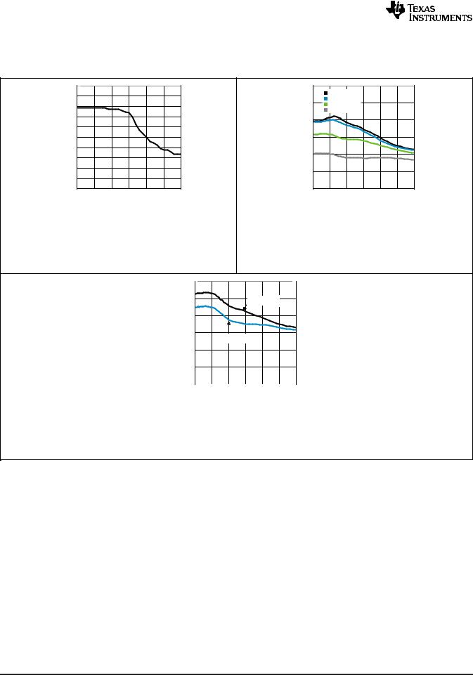
LMK04803, LMK04805, LMK04806, LMK04808
SNAS489K –MARCH 2011 –REVISED DECEMBER 2014 |
www.ti.com |
6.7 Typical Characteristics: Clock Output AC Characteristics
|
500 |
|
|
|
|
|
|
|
450 |
|
|
|
|
|
|
|
400 |
|
|
|
|
|
|
|
350 |
|
|
|
|
|
|
| <![if ! IE]> <![endif]>(mV) |
300 |
|
|
|
|
|
|
250 |
|
|
|
|
|
|
|
| <![if ! IE]> <![endif]>OD |
|
|
|
|
|
|
|
|
|
|
|
|
|
|
|
| <![if ! IE]> <![endif]>V |
200 |
|
|
|
|
|
|
|
|
|
|
|
|
|
|
|
150 |
|
|
|
|
|
|
|
100 |
|
|
|
|
|
|
|
50 |
|
|
|
|
|
|
|
0 |
|
|
|
|
|
|
|
0 |
500 |
1000 |
1500 |
2000 |
2500 |
3000 |
FREQUENCY (MHz)
Figure 1. LVDS VOD vs. Frequency
1200 |
|
|
2000 mVpp |
1000 |
1600 mVpp |
1200 mVpp |
|
|
700 mVpp |
| <![if ! IE]> <![endif]>(mV) |
800 |
|
|
|
|
|
|
600 |
|
|
|
|
|
|
|
| <![if ! IE]> <![endif]>OD |
|
|
|
|
|
|
|
|
|
|
|
|
|
|
|
| <![if ! IE]> <![endif]>V |
|
|
|
|
|
|
|
|
400 |
|
|
|
|
|
|
|
200 |
|
|
|
|
|
|
|
0 |
|
|
|
|
|
|
|
0 |
500 |
1000 |
1500 |
2000 |
2500 |
3000 |
FREQUENCY (MHz)
Figure 2. LVPECL /w 240-Ω Emitter Resistors VOD vs. Frequency
<![endif]>VOD(mV)
1200 |
|
1000 |
2000 mVpp |
|
|
800 |
|
600
1600 mVpp |
400
200
0
0 500 1000 1500 2000 2500 3000
FREQUENCY (MHz)
Figure 3. LVPECL /w 120-Ω Emitter Resistors VOD vs. Frequency
14 |
Submit Documentation Feedback |
Copyright © 2011–2014, Texas Instruments Incorporated |
Product Folder Links: LMK04803 LMK04805 LMK04806 LMK04808
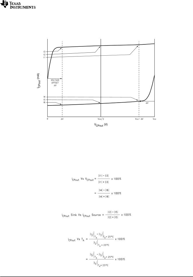
LMK04803, LMK04805, LMK04806, LMK04808
www.ti.com |
SNAS489K –MARCH 2011–REVISED DECEMBER 2014 |
7 Parameter Measurement Information
7.1 Charge Pump Current Specification Definitions
I1 |
= Charge Pump Sink Current at VCPout = VCC - V |
I2 |
= Charge Pump Sink Current at VCPout = VCC/2 |
I3 |
= Charge Pump Sink Current at VCPout = V |
I4 |
= Charge Pump Source Current at VCPout = VCC - V |
I5 |
= Charge Pump Source Current at VCPout = VCC/2 |
I6 |
= Charge Pump Source Current at VCPout = V |
V = Voltage offset from the positive and negative supply rails. Defined to be 0.5 V for this device.
7.1.1 Charge Pump Output Current Magnitude Variation Vs. Charge Pump Output Voltage
7.1.2Charge Pump Sink Current Vs. Charge Pump Output Source Current Mismatch
7.1.3Charge Pump Output Current Magnitude Variation vs. Ambient Temperature
Copyright © 2011–2014, Texas Instruments Incorporated |
Submit Documentation Feedback |
15 |
Product Folder Links: LMK04803 LMK04805 LMK04806 LMK04808
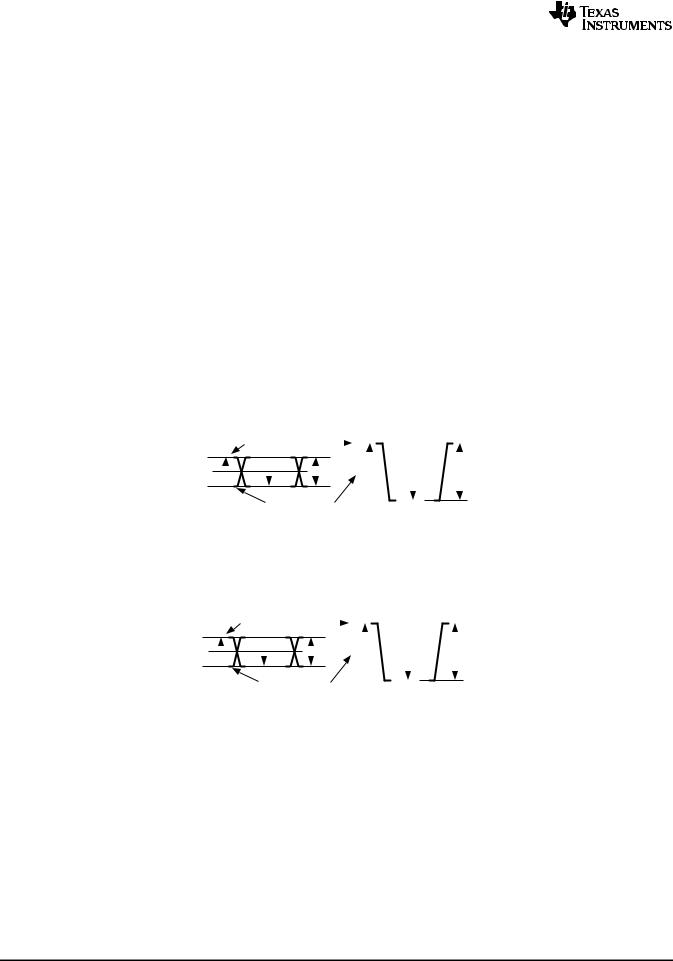
LMK04803, LMK04805, LMK04806, LMK04808
SNAS489K –MARCH 2011 –REVISED DECEMBER 2014 |
www.ti.com |
7.2 Differential Voltage Measurement Terminology
The differential voltage of a differential signal can be described by two different definitions causing confusion when reading datasheets or communicating with other engineers. This section will address the measurement and description of a differential signal so that the reader will be able to understand and discern between the two different definitions when used.
The first definition used to describe a differential signal is the absolute value of the voltage potential between the inverting and non-inverting signal. The symbol for this first measurement is typically VID or VOD depending on if an input or output voltage is being described.
The second definition used to describe a differential signal is to measure the potential of the non-inverting signal with respect to the inverting signal. The symbol for this second measurement is VSS and is a calculated parameter. Nowhere in the IC does this signal exist with respect to ground, it only exists in reference to its differential pair. VSS can be measured directly by oscilloscopes with floating references, otherwise this value can be calculated as twice the value of VOD as described in the first description.
Figure 4 illustrates the two different definitions side-by-side for inputs and Figure 5 illustrates the two different definitions side-by-side for outputs. The VID and VOD definitions show VA and VB DC levels that the non-inverting and inverting signals toggle between with respect to ground. VSS input and output definitions show that if the inverting signal is considered the voltage potential reference, the non-inverting signal voltage potential is now increasing and decreasing above and below the non-inverting reference. Thus the peak-to-peak voltage of the differential signal can be measured.
VID and VOD are often defined as volts (V) and VSS is often defined as volts peak-to-peak (VPP).
|
|
|
VID Definition |
VSS Definition for Input |
||||||||||||||||||
VA |
|
|
Non-Inverting Clock |
|
|
|
|
|
|
|
|
|
|
|
|
|||||||
|
|
|
|
|
|
|
|
|
|
|
2·VID |
|||||||||||
|
|
|
|
|
|
|
|
VID |
|
|
|
|
|
|
|
|
||||||
|
|
|
|
|
|
|
|
|
|
|
|
|
|
|
|
|||||||
|
|
|
|
|
|
|
|
|
|
|
|
|
|
|||||||||
VB |
|
|
|
|
|
|
|
|
|
|
|
|
|
|
|
|
||||||
|
|
|
|
|
|
|
|
|
|
|
|
|
|
|
||||||||
|
|
|
|
|
|
|
|
|
|
|
|
|
|
|
|
|
|
|
|
|
|
|
|
|
Inverting Clock |
|
|
|
|
|
|
|
|
|
|
||||||||||
|
|
|
|
|
|
|
|
|
|
|
|
|
|
|||||||||
|
|
|
|
|
|
VSS = 2·VID |
||||||||||||||||
|
|
|
VID = | VA - VB | |
|
|
|||||||||||||||||
GND |
|
|
|
|
|
|
|
|
|
|
|
|
|
|
|
|
|
|||||
|
|
|
|
|
|
|
|
|
|
|
|
|
|
|||||||||
Figure 4. Two Different Definitions for Differential Input Signals
|
|
|
VOD Definition |
VSS Definition for Output |
||||||||||||||||||
VA |
|
|
Non-Inverting Clock |
|
|
|
|
|
|
|
|
|
|
|
|
|||||||
|
|
|
|
|
|
|
|
|
|
|
2·VOD |
|||||||||||
|
|
|
|
|
|
|
|
|
VOD |
|
|
|
|
|
|
|
|
|||||
|
|
|
|
|
|
|
|
|
|
|
|
|
|
|
|
|
||||||
|
|
|
|
|
|
|
|
|
|
|
|
|
|
|||||||||
VB |
|
|
|
|
|
|
|
|
|
|
|
|
|
|
|
|
|
|||||
|
|
|
|
|
|
|
|
|
|
|
|
|
|
|
|
|||||||
|
|
|
|
|
|
|
|
|
|
|
|
|
|
|
|
|
|
|
|
|
|
|
|
|
Inverting Clock |
|
|
|
|
|
|
|
|
|
|
||||||||||
|
|
|
|
|
|
|
|
|
|
|
|
|
|
|||||||||
|
|
|
|
|
|
VSS = 2·VOD |
||||||||||||||||
|
|
VOD = | VA - VB | |
|
|
||||||||||||||||||
GND |
|
|
|
|
|
|
|
|
|
|
|
|
|
|
|
|
|
|||||
|
|
|
|
|
|
|
|
|
|
|
|
|
|
|||||||||
Figure 5. Two Different Definitions for Differential Output Signals
Refer to Application Note AN-912, Common Data Transmission Parameters and their Definitions (SNLA036) for more information.
16 |
Submit Documentation Feedback |
Copyright © 2011–2014, Texas Instruments Incorporated |
Product Folder Links: LMK04803 LMK04805 LMK04806 LMK04808

LMK04803, LMK04805, LMK04806, LMK04808
www.ti.com |
SNAS489K –MARCH 2011–REVISED DECEMBER 2014 |
8 Detailed Description
8.1 Overview
In default mode of operation, dual PLL mode with internal VCO, the Phase Frequency Detector in PLL1 compares the active CLKinX reference divided by CLKinX_PreR_DIV and PLL1 R divider with the external VCXO or crystal attached to the PLL2 OSCin port divided by PLL1 N divider. The external loop filter for PLL1 should be narrow to provide an ultra clean reference clock from the external VCXO or crystal to the OSCin/OSCin* pins for PLL2.
The Phase Frequency Detector in PLL2 compares the external VCXO or crystal to the internal VCO after the reference and feedback dividers. The VCXO or crystal on the OSCin input is divided by PLL2 R divider. The feedback from the internal VCO is divided by the PLL2 Prescaler, the PLL2 N divider, and optionally the VCO divider.
The bandwidth of the external loop filter for PLL2 should be designed to be wide enough to take advantage of the low in-band phase noise of PLL2 and the low high offset phase noise of the internal VCO. The VCO output is also placed on the distribution path for the Clock Distribution section. The clock distribution consists of 6 groups of dividers and delays which drive 12 outputs. Each clock group allows the user to select a divide value, a digital delay value, and an analog delay. The 6 groups drive programmable output buffers. Two groups allow their input signal to be from the OSCin port directly.
When a 0-delay mode is used, a clock output will be passed through the feedback mux to the PLL1 N Divider for synchronization and 0-delay.
When an external VCO mode is used, the Fin port will be used to input an external VCO signal. PLL2 Phase comparison will now be with this signal divided by the PLL2 N divider and N2 pre-scaler. The VCO divider may not be used. One less clock input is available when using an external VCO mode.
When a single PLL mode is used, PLL1 is powered down. OSCin is used as a reference to PLL2.
8.1.1 System Architecture
The dual loop PLL architecture of the LMK0480x provides the lowest jitter performance over the widest range of output frequencies and phase noise integration bandwidths. The first stage PLL (PLL1) is driven by an external reference clock and uses an external VCXO or tunable crystal to provide a frequency accurate, low phase noise reference clock for the second stage frequency multiplication PLL (PLL2). PLL1 typically uses a narrow loop bandwidth (10 Hz to 200 Hz) to retain the frequency accuracy of the reference clock input signal while at the same time suppressing the higher offset frequency phase noise that the reference clock may have accumulated along its path or from other circuits. This “cleaned” reference clock provides the reference input to PLL2.
The low phase noise reference provided to PLL2 allows PLL2 to operate with a wide loop bandwidth (50 kHz to 200 kHz). The loop bandwidth for PLL2 is chosen to take advantage of the superior high offset frequency phase noise profile of the internal VCO and the good low offset frequency phase noise of the reference VCXO or tunable crystal.
Ultra low jitter is achieved by allowing the external VCXO or crystal’s phase noise to dominate the final output phase noise at low offset frequencies and the internal (or external) VCO’s phase noise to dominate the final output phase noise at high offset frequencies. This results in best overall phase noise and jitter performance.
The LMK0480x allows subsets of the device to be used to increase the flexibility of device. These different modes are selected using MODE: Device Mode. For instance:
•Dual Loop Mode - Typical use case of LMK04808. CLKinX used as reference input to PLL1, OSCin port is connected to VCXO or tunable crystal.
•Single Loop Mode - Powers down PLL1. OSCin port is used as reference input.
•Clock Distribution Mode - Allows input of CLKin1 to be distributed to output with division, digital delay, and analog delay.
See Device Functional Modes for more information on these modes.
Copyright © 2011–2014, Texas Instruments Incorporated |
Submit Documentation Feedback |
17 |
Product Folder Links: LMK04803 LMK04805 LMK04806 LMK04808

LMK04803, LMK04805, LMK04806, LMK04808
SNAS489K –MARCH 2011 –REVISED DECEMBER 2014 |
www.ti.com |
Overview (continued)
8.1.2 PLL1 Redundant Reference Inputs (CLKin0/CLKin0* and CLKin1/CLKin1*)
The LMK0480x has two reference clock inputs for PLL1: CLKin0 and CLKin1. Ref Mux selects CLKin0 or CLKin1. Automatic or manual switching occurs between the inputs.
CLKin0 and CLKin1 each have input dividers. The input divider allows different clock input frequencies to be normalized so that the frequency input to the PLL1 R divider remains constant during automatic switching. By programming these dividers such that the frequency presented to the input of the PLL1_R divider is the same prevents the user from needing to reprogram the PLL1 R divider when the input reference is changed to another CLKin port with a different frequency.
CLKin1 is shared for use as an external 0-delay feedback (FBCLKin), or for use with an external VCO (Fin).
Fast manual switching between reference clocks is possible with external pins Status_CLKin0 and Status_CLKin1.
8.1.3 PLL1 Tunable Crystal Support
The LMK0480x integrates a crystal oscillator on PLL1 for use with an external crystal and varactor diode to perform jitter cleaning.
The LMK0480x must be programmed to enable Crystal mode.
8.1.4 VCXO/CRYSTAL Buffered Outputs
The LMK0480x provides 2 dedicated outputs which are a buffered copy of the PLL2 reference input. This reference input is typically a low noise VCXO or Crystal. When using a VCXO, this output can be used to clock external devices such as microcontrollers, FPGAs, CPLDs, and so forth, before the LMK0480x is programmed.
The OSCout0 buffer output type is programmable to LVDS, LVPECL, or LVCMOS. The OSCout1 buffer is fixed to LVPECL.
The dedicated output buffers OSCout0 and OSCout1 can output frequency lower than the VCXO or Crystal frequency by programming the OSC Divider. The OSC Divider value range is 2 to 8. Each OSCoutX can individually choose to use the OSC Divider output or to bypass the OSC Divider.
Two clock output groups can also be programmed to be driven by OSCin. This allows a total of 4 additional differential outputs to be buffered outputs of OSCin. When programmed in this way, a total of 6 differential outputs can be driven by a buffered copy of OSCin.
VCXO/Crystal buffered outputs cannot be synchronized to the VCO clock distribution outputs. The assertion of SYNC will still cause these outputs to become low temporarily. Since these outputs will turn off and on asynchronously with respect to the VCO sourced clock outputs during a SYNC, it is possible for glitches to occur on the buffered clock outputs when SYNC is asserted and unasserted. If the NO_SYNC_CLKoutX_Y bits are set these outputs will not be affected by the SYNC event except that the phase relationship will change with the other synchronized clocks unless a buffered clock output is used as a qualification clock during SYNC.
8.1.5 Frequency Holdover
The LMK0480x supports holdover operation to keep the clock outputs on frequency with minimum drift when the reference is lost until a valid reference clock signal is re-established.
8.1.6 Integrated Loop Filter Poles
The LMK0480x features programmable 3rd and 4th order loop filter poles for PLL2. These internal resistors and capacitor values may be selected from a fixed range of values to achieve either a 3rd or 4th order loop filter response. The integrated programmable resistors and capacitors compliment external components mounted near the chip.
These integrated components can be effectively disabled by programming the integrated resistors and capacitors to their minimum values.
18 |
Submit Documentation Feedback |
Copyright © 2011–2014, Texas Instruments Incorporated |
Product Folder Links: LMK04803 LMK04805 LMK04806 LMK04808

LMK04803, LMK04805, LMK04806, LMK04808
www.ti.com |
SNAS489K –MARCH 2011–REVISED DECEMBER 2014 |
Overview (continued)
8.1.7 Internal VCO
The output of the internal VCO is routed to a mux which allows the user to select either the direct VCO output or a divided version of the VCO for the Clock Distribution Path. This same selection is also fed back to the PLL2 phase detector through a prescaler and N-divider.
The mux selectable VCO divider has a divide range of 2 to 8 with 50% output duty cycle for both even and odd divide values.
The primary use of the VCO divider is to achieve divides greater than the clock output divider supports alone.
8.1.8 External VCO Mode
The Fin/Fin* input allows an external VCO to be used with PLL2 of the LMK0480x.
Using an external VCO reduces the number of available clock inputs by one.
8.1.9 Clock Distribution
The LMK0480x features a total of 12 outputs driven from the internal or external VCO.
All VCO driven outputs have programmable output types. They can be programmed to LVPECL, LVDS, or LVCMOS. When all distribution outputs are configured for LVCMOS or single ended LVPECL a total of 24 outputs are available.
If the buffered OSCin outputs OSCout0 and OSCout1 are included in the total number of clock outputs the LMK0480x is able to distribute, then up to 14 differential clocks or up to 28 single ended clocks may be generated with the LMK0480x.
The following sections discuss specific features of the clock distribution channels that allow the user to control various aspects of the output clocks.
8.1.9.1 CLKout DIVIDER
Each clock group, which is a pair of outputs such as CLKout0 and CLKout1, has a single clock output divider. The divider supports a divide range of 1 to 1045 (even and odd) with 50% output duty cycle. When divides of 26 or greater are used, the divider/delay block uses extended mode.
The VCO Divider may be used to reduce the divide needed by the clock group divider so that it may operate in normal mode instead of extended mode. This can result in a small current saving if enabling the VCO Divider allows 3 or more clock output divides to change from extended to normal mode.
8.1.9.2 CLKout Delay
See Clock Distribution section for details on both a fine (analog) and coarse (digital) delay for phase adjustment of the clock outputs.
The fine (analog) delay allows a nominal 25 ps step size and range from 0 to 475 ps of total delay. Enabling the analog delay adds a nominal 500 ps of delay in addition to the programmed value. When adjusting analog delay, glitches may occur on the clock outputs being adjusted. Analog delay may not operate at frequencies above the minimum-ensured maximum output frequency of 1536 MHz.
The coarse (digital) delay allows a group of outputs to be delayed by 4.5 to 12 clock distribution path cycles in normal mode, or from 12.5 to 522 VCO cycles in extended mode. The delay step can be as small as half the period of the clock distribution path by using the CLKoutX_Y_HS bit provided the output divide value is greater than 1. For example, a 2-GHz VCO frequency without the use of the VCO divider results in 250 ps coarse tuning steps.. The coarse (digital) delay value takes effect on the clock outputs after a SYNC event.
There are 3 different ways to use the digital (coarse) delay:
1.Fixed Digital Delay
2.Absolute Dynamic Digital Delay
3.Relative Dynamic Digital Delay
These are further discussed in Clock Distribution.
Copyright © 2011–2014, Texas Instruments Incorporated |
Submit Documentation Feedback |
19 |
Product Folder Links: LMK04803 LMK04805 LMK04806 LMK04808

LMK04803, LMK04805, LMK04806, LMK04808
SNAS489K –MARCH 2011 –REVISED DECEMBER 2014 |
www.ti.com |
Overview (continued)
8.1.9.3 Programmable Output Type
For increased flexibility all LMK0480x clock outputs (CLKoutX) and OSCout0 can be programmed to an LVDS, LVPECL, or LVCMOS output type. OSCout1 is fixed as LVPECL.
Any LVPECL output type can be programmed to 700, 1200, 1600, or 2000 mVpp amplitude levels. The 2000 mVpp LVPECL output type is a Texas Instruments proprietary configuration that produces a 2000 mVpp differential swing for compatibility with many data converters and is also known as 2VPECL.
8.1.9.4 Clock Output Synchronization
Using the SYNC input causes all active clock outputs to share a rising edge. See Clock Output Synchronization (SYNC) for more information.
The SYNC event also causes the digital delay values to take effect.
8.1.10 0-Delay
The 0-delay mode synchronizes the input clock phase to the output clock phase. The 0-delay feedback may be performed with an internal feedback loop from any of the clock groups or with an external feedback loop into the FBCLKin port as selected by the FEEDBACK_MUX.
Without using 0-delay mode there will be D possible fixed phase relationships from clock input to clock output depending on the clock output divide value.
Using an external 0-delay feedback reduces the number of available clock inputs by one.
8.1.11 Default Startup Clocks
Before the LMK0480x is programmed, CLKout8 is enabled and operating at a nominal frequency and CLKout6 and OSCout0 are enabled and operating at the OSCin frequency. These clocks can be used to clock external devices such as microcontrollers, FPGAs, CPLDs, and so forth, before the LMK0480x is programmed.
For CLKout6 and OSCout0 to work before the LMK0480x is programmed, the device must not be using Crystal mode.
8.1.12 Status Pins
The LMK0480x provides status pins which can be monitored for feedback or in some cases used for input depending upon device programming. For example:
•The Status_Holdover pin may indicate if the device is in hold-over mode.
•The Status_CLKin0 pin may indicate the LOS (loss-of-signal) for CLKin0.
•The Status_CLKin0 pin may be an input for selecting the active clock input.
•The Status_LD pin may indicate if the device is locked.
The status pins can be programmed to a variety of other outputs including analog lock detect, PLL divider outputs, combined PLL lock detect signals, PLL1 Vtune railing, readback, and so forth. Refer to the Programming of this datasheet for more information. Default pin programming is captured in Table 18.
8.1.13 Register Readback
Programmed registers may be read back using the MICROWIRE interface. For readback, one of the status pins must be programmed for readback mode.
At no time may registers be programed to values other than the valid states defined in the datasheet.
20 |
Submit Documentation Feedback |
Copyright © 2011–2014, Texas Instruments Incorporated |
Product Folder Links: LMK04803 LMK04805 LMK04806 LMK04808

LMK04803, LMK04805, LMK04806, LMK04808
www.ti.com |
SNAS489K –MARCH 2011–REVISED DECEMBER 2014 |
8.2 Functional Block Diagram
CLKin0* |
CLKin0 Divider |
Ref |
R Delay |
|
CLKin0 |
(1, 2, 4, or 8) |
Mux |
||
|
||||
CLKin1*/Fin* |
CLKin1 Divider |
|
|
|
FBCLKin* |
|
N Delay |
||
CLKin1/ |
(1, 2, 4, or 8) |
|
||
|
|
|||
|
|
|
||
Fin/FBCLKin |
Fin/Fin* |
FBMux |
|
|
|
|
CLKout0
CLKout2
CLKout4
FB
CLKout6
Mux Mode
CLKout8 Mux2
CLKout10
OSCout0 |
OSCout0 |
OSC Divider |
|
OSCout0* |
_MUX |
(2 to 8) |
|
|
|
FBMux |
Mode |
|
|
Mux3 |
|
OSCout1 |
OSCout1 |
|
|
|
|
||
OSCout1* |
_MUX |
|
|
OSCin* |
|
|
|
OSCin |
|
|
|
CLKout0 |
Mux |
|
|
CLKout0* |
|
||
|
|
||
Clock Group 0 |
Divider |
Digital |
|
(1 to 1045) |
Delay |
||
|
|||
CLKout1 |
Delay |
|
|
Mux |
|
||
CLKout1* |
|
||
Clock Buffer 1 |
|||
|
|||
CLKout2 |
Mux |
|
|
CLKout2* |
|
||
|
|
||
Clock Group 1 |
Divider |
Digital |
|
(1 to 1045) |
Delay |
||
|
|||
CLKout3 |
Delay |
|
|
CLKout3* |
Mux |
|
|
|
|
||
CLKout4 |
Mux |
|
|
CLKout4* |
|
||
|
|
||
Clock Group 2 |
Divider |
Digital |
|
(1 to 1045) |
Delay |
||
|
|||
CLKout5 |
Delay |
|
|
Mux |
|
||
CLKout5* |
|
||
Clock Buffer 2 |
|||
|
|||
R1 Divider (1 to 16,383)
N1 Divider (1 to 16,383)
Phase |
<![if ! IE]> <![endif]>CPout1 |
|
|
Status_LD |
|
|
|
||
SYNC |
|
Device |
Status_Holdover |
|
Detector |
|
|||
|
|
Control |
Status_CLKin0 |
|
PLL1 |
|
|
||
|
|
|
||
|
|
|
|
|
|
|
|
|
Status_CLKin1 |
|
CLKuWire |
|
|
|
Holdover |
DATAuWire |
PWire |
Control |
|
Port |
Registers |
|
||
|
LEuWire |
|
||
|
|
|
|
2X |
|
|
|
|
|
|
|
|
|
<![if ! IE]> <![endif]>CPout2 |
Partially |
|
|
|
|
|
|||||||
|
|
|
|
|
|
|
|
|
|
|
|
|
|||||||||||
|
|
|
2X |
R2 Divider |
|
|
|
|
|
|
Integrated |
|
|
|
|
|
|||||||
|
|
|
|
|
|
|
|
|
|
|
|
|
|
||||||||||
|
|
|
Mux |
|
|
(1 to 4,095) |
|
Phase |
|
|
|
|
Loop Filter |
Internal VCO |
|||||||||
|
|
|
|
|
|
|
|
Detector |
|
|
|
|
|
|
|
|
|
|
|
|
|
||
|
|
|
|
|
|
|
|
PLL2 |
|
|
|
|
|
|
|
|
|
|
|
|
|
|
|
|
|
|
|
|
|
N2 Divider |
|
|
|
|
|
|
|
|
|
|
|
|
|
|
|
|
|
|
|
|
|
|
|
(1 to 262,143) |
|
|
|
|
|
|
|
|
|
|
|
|
|
|
|
|
|
|
|
|
|
|
|
|
|
|
|
|
|
|
|
|
|
|
|
|
|
|
|
|
|
|
|
|
|
|
|
|
|
|
|
|
|
|
|
|
|
|
|
|
|
|
|
|
|
|
|
|
|
|
|
|
|
|
|
|
|
|
VCO |
|
|
|
|
|
|||||
|
|
|
|
|
|
|
|
|
|
|
|
|
|
|
|
|
|
|
VCO Divider |
|
|||
|
N2 Prescaler |
|
Clock Distribution Path |
Mode |
|
Mux |
|
|
|
||||||||||||||
|
|
|
|
|
|
|
|
(2 to 8) |
|
|
|
||||||||||||
|
|
|
(2 to 8) |
|
|
|
|
|
|
|
|
|
|
|
|
|
|
|
|
|
|||
|
|
|
|
|
|
|
Mux1 |
|
|
|
|
|
|
|
|
|
|||||||
|
|
|
|
|
|
|
|
|
|
|
|
|
|
|
|
|
|
||||||
|
|
|
|
|
|
|
|
|
|
|
|
|
|
|
|
|
|
|
|
|
|
|
|
|
|
|
|
Fin/Fin* |
|
|
|
|
CLKout6 |
|
|
|
|
Mux |
Osc |
Digital |
Divider |
|
CLKout6* |
Mux1 |
|
Clock Group 3 |
||
|
Delay |
(1 to 1045) |
|
|
|
Delay |
CLKout7 |
||
|
|
|
||
|
|
|
|
Mux |
|
|
|
|
CLKout7* |
|
|
|
|
CLKout8 |
|
|
|
|
Mux |
Osc |
Digital |
Divider |
|
CLKout8* |
Mux2 |
|
Clock Group 4 |
||
Delay |
(1 to 1045) |
|
||
|
|
|||
|
Delay |
CLKout9 |
||
|
|
|
||
Clock Buffer 3 |
|
|
Mux |
|
|
|
CLKout9* |
||
|
|
|
|
CLKout10 |
|
|
|
|
Mux |
|
|
|
|
CLKout10* |
|
Digital |
Divider |
|
Clock Group 5 |
|
Delay |
(1 to 1045) |
|
|
|
Delay |
CLKout11 |
||
|
|
|
||
|
|
|
|
Mux |
Clock Buffer 1 |
|
|
CLKout11* |
|
|
|
|
||
Copyright © 2011–2014, Texas Instruments Incorporated |
Submit Documentation Feedback |
21 |
Product Folder Links: LMK04803 LMK04805 LMK04806 LMK04808
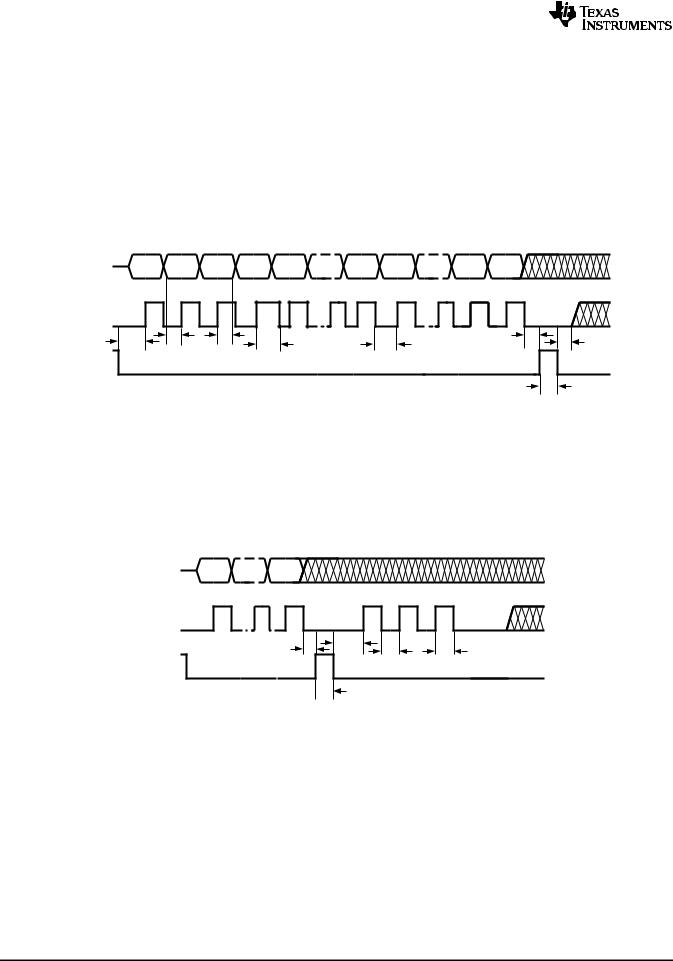
LMK04803, LMK04805, LMK04806, LMK04808
SNAS489K –MARCH 2011 –REVISED DECEMBER 2014 |
www.ti.com |
8.3 Feature Description
8.3.1 Serial MICROWIRE Timing Diagram
For timing specifications, see Timing Requirements. Register programming information on the DATAuWire pin is clocked into a shift register on each rising edge of the CLKuWire signal. On the rising edge of the LEuWire signal, the register is sent from the shift register to the register addressed. A slew rate of at least 30 V/µs is recommended for these signals. After programming is complete the CLKuWire, DATAuWire, and LEuWire signals should be returned to a low state. If the CLKuWire or DATAuWire lines are toggled while the VCO is in lock, as is sometimes the case when these lines are shared with other parts, the phase noise may be degraded during this programming.
|
MSB |
|
|
|
|
|
|
|
LSB |
DATAuWire |
D26 |
D25 |
D24 |
D23 |
D22 |
D0 |
A4 |
A1 |
A0 |
CLKuWire |
|
|
|
|
|
|
|
|
|
|
tECS |
|
|
|
|
|
|
|
tCES |
|
tDCS |
tCDH |
tCWH |
|
|
tCWL |
|
tECS |
|
|
|
|
|
|
|
||||
|
|
|
|
|
|
|
|
||
LEuWire |
|
|
|
|
|
|
|
|
|
|
|
|
|
|
|
|
|
|
tEWH |
Figure 6. MICROWIRE Input Timing Diagram
8.3.2 Advanced MICROWIRE Timing Diagrams
8.3.2.1 Three Extra Clocks or Double Program
For timing specifications, see Timing Requirements. Figure 7 shows the timing for the programming sequence for loading CLKoutX_Y_DIV > 25 or CLKoutX_Y_DDLY > 12 as described in Special Programming Case for R0 to R5 for CLKoutX_Y_DIV and CLKoutX_Y_DDLY.
|
MSB |
LSB |
DATAuWire |
D26 |
A0 |
CLKuWire
tECS
tCES
tCWL tCWH
LEuWire
tEWH 
Figure 7. MICROWIRE Timing Diagram: Extra CLKuWire Pulses for R0 to R5
22 |
Submit Documentation Feedback |
Copyright © 2011–2014, Texas Instruments Incorporated |
Product Folder Links: LMK04803 LMK04805 LMK04806 LMK04808
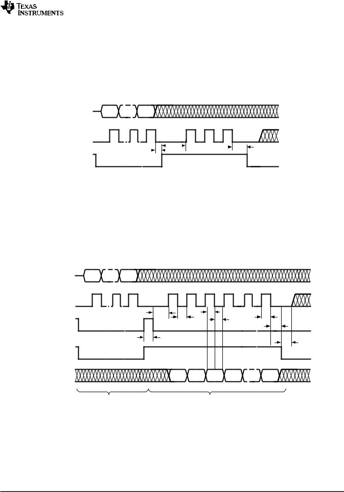
LMK04803, LMK04805, LMK04806, LMK04808
www.ti.com |
SNAS489K –MARCH 2011–REVISED DECEMBER 2014 |
Feature Description (continued)
8.3.2.2 Three Extra Clocks with LEuWire High
For timing specifications, see Timing Requirements. Figure 8 shows the timing for the programming sequence which allows SYNC_EN_AUTO = 1 when loading CLKoutX_Y_DIV > 25 or CLKoutX_Y_DDLY > 12. When SYNC_EN_AUTO = 1, a SYNC event is automatically generated on the falling edge of LEuWire. See Special Programming Case for R0 to R5 for CLKoutX_Y_DIV and CLKoutX_Y_DDLY.
|
MSB |
LSB |
DATAuWire |
D26 |
A0 |
CLKuWire
tCES |
|
|
|
tECS |
|
|
|
tCES |
|
|
|
|
|
||||
|
||||||||
|
|
|
|
|
|
|
|
LEuWire
Figure 8. MICROWIRE Timing Diagram: Extra CLKuWire Pulses for R0 to R5 with LEuWire Asserted
8.3.2.3 Readback
For timing specifications, see Timing Requirements. See Readback for more information on performing a readback operation. Figure 9 shows timing for LEuWire for both READBACK_LE = 1 and 0.
The rising edges of CLKuWire during MICROWIRE readback continue to clock data on DATAuWire into the device during readback. If after the readback, LEuWire transitions from low to high, this data will be latched to the decoded register. The decoded register address consists of the last 5 bits clocked on DATAuWire as shown in Figure 9.
|
MSB |
LSB |
|
|
DATAuWire |
D26 |
A0 |
|
|
CLKuWire |
|
|
|
|
|
|
tECS |
tCR |
tCWH |
|
|
tCWL |
tCR |
|
LEuWire |
|
|
||
|
|
tCES |
||
READBACK_LE = 0 |
|
|
|
|
|
|
tEWH |
|
|
|
|
|
|
tECS |
LEuWire |
|
|
|
|
READBACK_LE = 1 |
|
|
|
|
Readback Pin |
|
RD26 |
RD25 RD24 RD23 |
RD0 |
|
Register Write |
|
Register Read |
|
Figure 9. MICROWIRE Readback Timing Diagram
8.3.3 Inputs / Outputs
8.3.3.1 PLL1 Reference Inputs (CLKin0 and CLKin1)
The reference clock inputs for PLL1 may be selected from either CLKin0 or CLKin1. The user has the capability to manually select one of the inputs or to configure an automatic switching mode of operation. See Input Clock Switching for more info.
Copyright © 2011–2014, Texas Instruments Incorporated |
Submit Documentation Feedback |
23 |
Product Folder Links: LMK04803 LMK04805 LMK04806 LMK04808

LMK04803, LMK04805, LMK04806, LMK04808
SNAS489K –MARCH 2011 –REVISED DECEMBER 2014 |
www.ti.com |
Feature Description (continued)
CLKin0 and CLKin1 have dividers which allow the device to switch between reference inputs of different frequencies automatically without needing to reprogram the PLL1 R divider. The CLKin pre-divider values are 1, 2, 4, and 8.
CLKin1 input can alternatively be used for external feedback in 0-delay mode (FBCLKin) or for an external VCO input port (Fin).
8.3.3.2 PLL2 OSCin / OSCin* Port
The feedback from the external oscillator being locked with PLL1 drives the OSCin/OSCin* pins. Internally this signal is routed to the PLL1 N Divider and to the reference input for PLL2.
This input may be driven with either a single-ended or differential signal and must be AC coupled. If operated in single ended mode, the unused input must be connected to GND with a 0.1 µF capacitor.
8.3.3.3 Crystal Oscillator
The internal circuitry of the OSCin port also supports the optional implementation of a crystal based oscillator circuit. A crystal, a varactor diode, and a small number of other external components may be used to implement the oscillator. The internal oscillator circuit is enabled by setting the EN_PLL2_XTAL bit. See EN_PLL2_XTAL.
8.3.4 Input Clock Switching
Manual, pin select, and automatic are three different kinds clock input switching modes can be set with the CLKin_SELECT_MODE register.
Below is information about how the active input clock is selected and what causes a switching event in the various clock input selection modes.
8.3.4.1 Input Clock Switching - Manual Mode
When CLKin_SELECT_MODE is 0 or 1 then CLKin0 or CLKin1 respectively is always selected as the active input clock. Manual mode will also override the EN_CLKinX bits such that the CLKinX buffer will operate even if CLKinX is disabled with EN_CLKinX = 0.
•Entering Holdover: If holdover mode is enabled, then holdover mode is entered if Digital lock detect of PLL1 goes low and DISABLE_DLD1_DET = 0.
•Exiting Holdover: The active clock for automatic exit of holdover mode is the manually selected clock input.
8.3.4.2 Input Clock Switching - Pin Select Mode
When CLKin_SELECT_MODE is 3, the pins Status_CLKin0 and Status_CLKin1 select which clock input is active.
•Clock Switch Event: Pins: Changing the state of Status_CLKin0 or Status_CLKin1 pins causes an input clock switch event.
•Clock Switch Event: PLL1 DLD: To prevent PLL1 DLD high to low transition from causing a input clock switch event and causing the device to enter holdover mode, disable the PLL1 DLD detect by setting DISABLE_DLD1_DET = 1. This is the preferred behavior for Pin Select Mode.
•Configuring Pin Select Mode:
–The Status_CLKin0_TYPE must be programmed to an input value for the Status_CLKin0 pin to function as an input for pin select mode.
–The Status_CLKin1_TYPE must be programmed to an input value for the Status_CLKin1 pin to function as an input for pin select mode.
–If the Status_CLKinX_TYPE is set as output, the input value is considered 0.
–The polarity of Status_CLKin1 and Status_CLKin0 input pins cannot be inverted with the CLKin_SEL_INV bit.
–Table 1 defines which input clock is active depending on Status_CLKin0 and Status_CLKin1 state.
24 |
Submit Documentation Feedback |
Copyright © 2011–2014, Texas Instruments Incorporated |
Product Folder Links: LMK04803 LMK04805 LMK04806 LMK04808

|
LMK04803, LMK04805, LMK04806, LMK04808 |
www.ti.com |
SNAS489K –MARCH 2011–REVISED DECEMBER 2014 |
Feature Description (continued)
Table 1. Active Clock Input - Pin Select Mode
STATUS_CLKin1 |
STATUS_CLKin0 |
ACTIVE CLOCK |
0 |
0 |
CLKin0 |
0 |
1 |
CLKin1 |
1 |
0 |
Reserved |
1 |
1 |
Holdover |
The pin select mode will override the EN_CLKinX bits such that the CLKinX buffer will operate even if CLKinX is disabled with EN_CLKinX = 0. To switch as fast as possible, keep the clock input buffers enabled (EN_CLKinX = 1) that could be switched to.
8.3.4.2.1 Pin Select Mode and Host
When in the pin select mode, the host can monitor conditions of the clocking system which could cause the host to switch the active clock input. The LMK0480x device can also provide indicators on the Status_LD and Status_HOLDOVER like "DAC Rail," "PLL1 DLD", "PLL1 and PLL2 DLD" which the host can use in determining which clock input to use as active clock input.
8.3.4.2.2 Switch Event without Holdover
When an input clock switch event is triggered and holdover mode is disabled, the active clock input immediately switches to the selected clock. When PLL1 is designed with a narrow loop bandwidth, the switching transient is minimized.
8.3.4.2.3 Switch Event with Holdover
When an input clock switch event is triggered and holdover mode is enabled, the device will enter holdover mode and remain in holdover until a holdover exit condition is met as described in Holdover Mode. Then the device will complete the reference switch to the pin selected clock input.
8.3.4.3 Input Clock Switching - Automatic Mode
When CLKin_SELECT_MODE is 4, the active clock is selected in priority order of enabled clock inputs starting upon an input clock switch event. The priority order of the clocks is CLKin0 → CLKin1 → CLKin0, and so forth.
For a clock input to be eligible to be switched through, it must be enabled using EN_CLKinX.
8.3.4.3.1 Starting Active Clock
Upon programming this mode, the currently active clock remains active if PLL1 lock detect is high. To ensure a particular clock input is the active clock when starting this mode, program CLKin_SELECT_MODE to the manual mode which selects the desired clock input (CLKin0 or 1). Wait for PLL1 to lock PLL1_DLD = 1, then select this mode with CLKin_SELECT_MODE = 4.
8.3.4.3.2 Clock Switch Event: PLL1 DLD
A loss of lock as indicated by PLL1’s DLD signal (PLL1_DLD = 0) will cause an input clock switch event if DISABLE_DLD1_DET = 0. PLL1 DLD must go high (PLL1_DLD = 1) in between input clock switching events.
8.3.4.3.3 Clock Switch Event: PLL1 Vtune Rail
If Vtune_RAIL_DET_EN is set and the PLL1 Vtune voltage crosses the DAC high or low threshold, holdover mode will be entered. Since PLL1_DLD = 0 in holdover a clock input switching event will occur.
8.3.4.3.4 Clock Switch Event with Holdover
Clock switch event with holdover enabled is recommended in this input clock switching mode. When an input clock switch event occurs, holdover mode is entered and the active clock is set to the clock input defined by the Status_CLKinX pins. When the new active clock meets the holdover exit conditions, holdover is exited and the active clock will continue to be used as a reference until another input clock switch event. PLL1 DLD must go high in between input clock switching events.
Copyright © 2011–2014, Texas Instruments Incorporated |
Submit Documentation Feedback |
25 |
Product Folder Links: LMK04803 LMK04805 LMK04806 LMK04808

LMK04803, LMK04805, LMK04806, LMK04808
SNAS489K –MARCH 2011 –REVISED DECEMBER 2014 |
www.ti.com |
8.3.4.4 Input Clock Switching - Automatic Mode with Pin Select
When CLKin_SELECT_MODE is 6, the active clock is selected using the Status_CLKinX pins upon an input clock switch event according to Table 2.
8.3.4.4.1 Starting Active Clock
Upon programming this mode, the currently active clock remains active if PLL1 lock detect is high. To ensure a particular clock input is the active clock when starting this mode, program CLKin_SELECT_MODE to the manual mode which selects the desired clock input (CLKin0 or 1). Wait for PLL1 to lock PLL1_DLD = 1, then select this mode with CLKin_SELECT_MODE = 6.
8.3.4.4.2 Clock Switch Event: PLL1 DLD
An input clock switch event is generated by a loss of lock as indicated by PLL1's DLD signal (PLL1 DLD = 0).
8.3.4.4.3 Clock Switch Event: PLL1 Vtune Rail
If Vtune_RAIL_DET_EN is set and the PLL1 Vtune voltage crosses the DAC threshold, holdover mode will be entered. Since PLL1_DLD = 0 in holdover, a clock input switching event will occur.
8.3.4.4.4 Clock Switch Event with Holdover
Clock switch event with holdover enabled is recommended in this input clock switching mode. When an input clock switch event occurs, holdover mode is entered and the active clock is set to the clock input defined by the Status_CLKinX pins. When the new active clock meets the holdover exit conditions, holdover is exited and the active clock will continue to be used as a reference until another input clock switch event. PLL1 DLD must go high in between input clock switching events."
Table 2. Active Clock Input - Auto Pin Mode
STATUS_CLKin1(1) |
STATUS_CLKin0 |
ACTIVE CLOCK |
X |
1 |
CLKin0 |
1 |
0 |
CLKin1 |
0 |
0 |
Reserved |
(1)The polarity of Status_CLKin1 and Status_CLKin0 input pins can be inverted with the CLKin_SEL_INV bit.
8.3.5 Holdover Mode
Holdover mode causes PLL2 to stay locked on frequency with minimal frequency drift when an input clock reference to PLL1 becomes invalid. While in holdover mode, the PLL1 charge pump is TRI-STATED and a fixed tuning voltage is set on CPout1 to operate PLL1 in open loop.
8.3.5.1 Enable Holdover
Program HOLDOVER_MODE to enable holdover mode. Holdover mode can be manually enabled by programming the FORCE_HOLDOVER bit.
The holdover mode can be set to operate in 2 different sub-modes.
•Fixed CPout1 (EN_TRACK = 0 or 1, EN_MAN_DAC = 1).
•Tracked CPout1 (EN_TRACK = 1, EN_MAN_DAC = 0).
– Not valid when EN_VTUNE_RAIL_DET = 1.
Updates to the DAC value for the Tracked CPout1 sub-mode occurs at the rate of the PLL1 phase detector frequency divided by DAC_CLK_DIV. These updates occur any time EN_TRACK = 1.
The DAC update rate should be programmed for <= 100 kHz to ensure DAC holdover accuracy.
When tracking is enabled the current voltage of DAC can be readback, see DAC_CNT.
26 |
Submit Documentation Feedback |
Copyright © 2011–2014, Texas Instruments Incorporated |
Product Folder Links: LMK04803 LMK04805 LMK04806 LMK04808

LMK04803, LMK04805, LMK04806, LMK04808
www.ti.com |
SNAS489K –MARCH 2011–REVISED DECEMBER 2014 |
8.3.5.2 Entering Holdover
The holdover mode is entered as described in Input Clock Switching. Typically this is because:
•FORCE_HOLDOVER bit is set.
•PLL1 loses lock according to PLL1_DLD, and
–HOLDOVER_MODE = 2
–DISABLE_DLD1_DET = 0
•CPout1 voltage crosses DAC high or low threshold, and
–HOLDOVER_MODE = 2
–EN_VTUNE_RAIL_DET = 1
–EN_TRACK = 1
–DAC_HIGH_TRIP = User Value
–DAC_LOW_TRIP = User Value
–EN_MAN_DAC = 1
–MAN_DAC = User Value
8.3.5.3 During Holdover
PLL1 is run in open loop mode.
•PLL1 charge pump is set to TRI-STATE.
•PLL1 DLD will be unasserted.
•The HOLDOVER status is asserted
•During holdover If PLL2 was locked prior to entry of holdover mode, PLL2 DLD will continue to be asserted.
•CPout1 voltage will be set to:
–a voltage set in the MAN_DAC register (fixed CPout1).
–a voltage determined to be the last valid CPout1 voltage (tracked CPout1).
•PLL1 DLD will attempt to lock with the active clock input.
The HOLDOVER status signal can be monitored on the Status_HOLDOVER or Status_LD pin by programming the HOLDOVER_MUX or LD_MUX register to "Holdover Status."
8.3.5.4 Exiting Holdover
Holdover mode can be exited in one of two ways.
•Manually, by programming the device from the host.
•Automatically, By a clock operating within a specified ppm of the current PLL1 frequency on the active clock input. See Input Clock Switching for more detail on which clock input is active.
To exit holdover by programming, set HOLDOVER_MODE = Disabled. HOLDOVER_MODE can then be reenabled by programming HOLDOVER_MODE = Enabled. Care should be taken to ensure that the active clock upon exiting holdover is as expected, otherwise the CLKin_SELECT_MODE register may need to be reprogrammed.
Copyright © 2011–2014, Texas Instruments Incorporated |
Submit Documentation Feedback |
27 |
Product Folder Links: LMK04803 LMK04805 LMK04806 LMK04808

LMK04803, LMK04805, LMK04806, LMK04808
SNAS489K –MARCH 2011 –REVISED DECEMBER 2014 |
www.ti.com |
8.3.5.5 Holdover Frequency Accuracy and DAC Performance
When in holdover mode PLL1 will run in open loop and the DAC will set the CPout1 voltage. If Fixed CPout1 mode is used, then the output of the DAC will be a voltage dependant upon the MAN_DAC register. If Tracked CPout1 mode is used, then the output of the DAC will be the voltage at the CPout1 pin before holdover mode was entered. When using Tracked mode and EN_MAN_DAC = 1, during holdover the DAC value is loaded with the programmed value in MAN_DAC, not the tracked value.
When in Tracked CPout1 mode the DAC has a worst case tracking error of ±2 LSBs once PLL1 tuning voltage is acquired. The step size is approximately 3.2 mV, therefore the VCXO frequency error during holdover mode caused by the DAC tracking accuracy is ±6.4 mV × Kv, where Kv is the tuning sensitivity of the VCXO in use. Therefore the accuracy of the system when in holdover mode in ppm is:
Holdover accuracy (ppm) = |
± 6.4 mV × Kv × 1e6 |
|
|
VCXO Frequency |
(1) |
||
|
Example: consider a system with a 19.2-MHz clock input, a 153.6-MHz VCXO with a Kv of 17 kHz/V. The accuracy of the system in holdover in ppm is:
±0.71ppm |
= |
±6.4 mV ´ 17 kHz / V ´ 1e6 |
|
|
|
(2) |
|||
153.6 MHz |
||||
|
|
It is important to account for this frequency error when determining the allowable frequency error window to cause holdover mode to exit.
8.3.5.6 Holdover Mode - Automatic Exit of Holdover
The LMK0480x device can be programmed to automatically exit holdover mode when the accuracy of the frequency on the active clock input achieves a specified accuracy. The programmable variables include PLL1_WND_SIZE and DLD_HOLD_CNT.
See Digital Lock Detect Frequency Accuracy to calculate the register values to cause holdover to automatically exit upon reference signal recovery to within a user specified ppm error of the holdover frequency.
It is possible for the time to exit holdover to vary because the condition for automatic holdover exit is for the reference and feedback signals to have a time/phase error less than a programmable value. Because it is possible for two clock signals to be very close in frequency but not close in phase, it may take a long time for the phases of the clocks to align themselves within the allowable time/phase error before holdover exits.
8.3.6 PLLs
8.3.6.1 PLL1
The maximum phase detector frequency (fPD1) of PLL1 is 40 MHz. Since a narrow loop bandwidth should be used for PLL1, the need to operate at high phase detector rate to lower the in-band phase noise becomes unnecessary. The maximum values for the PLL1 R and N dividers is 16,383. Charge pump current ranges from 100 to 1600 µA. PLL1 N divider may be driven by OSCin port at the OSCout0_MUX output (default) or by internal or external feedback as selected by Feedback Mux in 0-delay mode.
Low charge pump currents and phase detector frequencies aid design of low loop bandwidth loop filters with reasonably sized components to allow the VCXO or PLL2 to dominate phase noise inside of PLL2 loop bandwidth. High charge pump currents may be used by PLL1 when using VCXOs with leaky tuning voltage inputs to improve system performance.
8.3.6.2 PLL2
PLL2's maximum phase detector frequency (fPD2) is 155 MHz. Operating at highest possible phase detector rate will ensure low in-band phase noise for PLL2 which in turn produces lower total jitter. The in-band phase noise from the reference input and PLL is proportional to N2. The maximum value for the PLL2 R divider is 4,095. The maximum value for the PLL2 N divider is 262,143. The N2 Prescaler in the total N feedback path can be programmed for values 2 to 8 (all divides even and odd). Charge pump current ranges from 100 to 3200 µA.
High charge pump currents help to widen the PLL2 loop bandwidth to optimize PLL2 performance.
28 |
Submit Documentation Feedback |
Copyright © 2011–2014, Texas Instruments Incorporated |
Product Folder Links: LMK04803 LMK04805 LMK04806 LMK04808
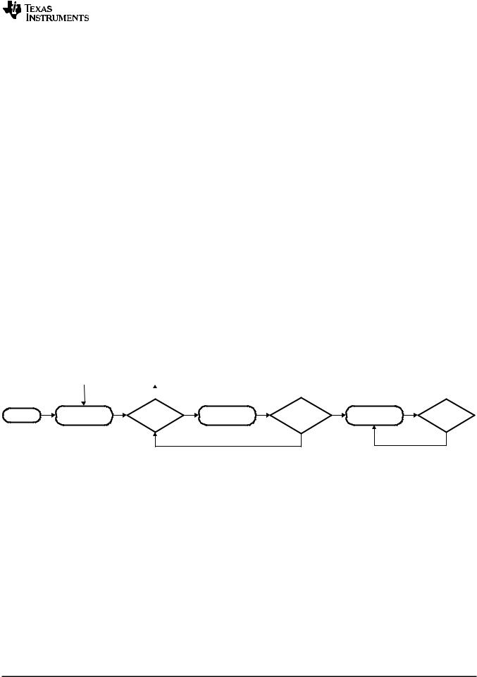
LMK04803, LMK04805, LMK04806, LMK04808
www.ti.com |
SNAS489K –MARCH 2011–REVISED DECEMBER 2014 |
8.3.6.2.1 PLL2 Frequency Doubler
The PLL2 reference input at the OSCin port may be routed through a frequency doubler before the PLL2 R Divider. The frequency doubler feature allows the phase comparison frequency to be increased when a relatively low frequency oscillator is driving the OSCin port. By doubling the PLL2 phase detector frequency, the in-band PLL2 noise is reduced by about 3 dB.
When using the doubler, PLL2 R Divider may be used to reduce the phase detector frequency to the limit of the PLL2 maximum phase detector frequency.
For applications in which the OSCin frequency and PLL2 phase detector frequency are equal, the best PLL2 inband noise can be achieved when the doubler is enabled (EN_PLL2_REF_2X = 1) and the PLL2 R divide value is 2. Do not use doubler disabled (EN_PLL2_REF_2X = 0) and PLL2 R divide value of 1.
8.3.6.3 Digital Lock Detect
Both PLL1 and PLL2 support digital lock detect. Digital lock detect compares the phase between the reference path (R) and the feedback path (N) of the PLL. When the time error, which is phase error, between the two signals is less than a specified window size (ε) a lock detect count increments. When the lock detect count reaches a user specified value lock detect is asserted true. Once digital lock detect is true, a single phase comparison outside the specified window will cause digital lock detect to be asserted false. This is illustrated in Figure 10.
The incremental lock detect count feature functions as a digital filter to ensure that lock detect isn't asserted for only a brief time when the phases of R and N are within the specified tolerance for only a brief time during initial phase lock.
The digital lock detect signal can be monitored on the Status_LD or Status_Holdover pin. The pin may be programmed to output the status of lock detect for PLL1, PLL2, or both PLL1 and PLL2.
See Digital Lock Detect Frequency Accuracy for more detailed information on programming the registers to achieve a specified frequency accuracy in ppm with lock detect.
The digital lock detect feature can also be used with holdover to automatically exit holdover mode. See Holdover Mode for more info.
|
NO |
NO |
|
||
|
|
|
|
PLLX |
|
YES |
INCREMENT |
PLLX LOCK COUNT = |
YES |
PLLX |
|
START |
LOCK DETECTED = FALSE |
PHASE ERROR < g |
|
|
PHASE ERROR < g |
|||
|
PLLX LOCK COUNT |
PLLX_DLD_CNT |
|
LOCK DETECTED = TRUE |
||||
|
LOCK COUNT = 0 |
|
|
|
|
|||
|
|
|
|
|
|
|
|
|
|
|
|
|
|
NO |
|
|
YES |
Figure 10. Digital Lock Detect Flowchart
8.3.7 Status Pins
The Status_LD, Status_HOLDOVER, Status_CLKin0, Status_CLKin1, and SYNC pins can be programmed to output a variety of signals for indicating various statuses like digital lock detect, holdover, several DAC indicators, and several PLL divider outputs.
8.3.7.1 Logic Low
This is a vary simple output. In combination with the output _MUX register, this output can be toggled between high and low. Useful to confirm MICROWIRE programming or as a general purpose IO.
8.3.7.2 Digital Lock Detect
PLL1 DLD, PLL2 DLD, and PLL1 + PLL2 are selectable on certain output pins. See Digital Lock Detect for more information.
8.3.7.3 Holdover Status
Indicates if the device is in Holdover mode. See HOLDOVER_MODE for more information.
Copyright © 2011–2014, Texas Instruments Incorporated |
Submit Documentation Feedback |
29 |
Product Folder Links: LMK04803 LMK04805 LMK04806 LMK04808

LMK04803, LMK04805, LMK04806, LMK04808
SNAS489K –MARCH 2011 –REVISED DECEMBER 2014 |
www.ti.com |
8.3.7.4 DAC
Various flags for the DAC can be monitored including DAC Locked, DAC Rail, DAC Low, and DAC High.
When the PLL1 tuning voltage crosses the low threshold, DAC Low is asserted. When PLL1 tuning voltage crosses the high threshold, DAC High is asserted. When either DAC Low or DAC High is asserted, DAC Rail will also be asserted.
DAC Locked is asserted when EN_Track = 1 and DAC is closely tracking the PLL1 tuning voltage.
8.3.7.5 PLL Divider Outputs
The PLL divider outputs are useful for debugging failure to lock issues. It allows the user to measure the frequency the PLL inputs are receiving. The settings of PLL1_R, PLL1_N, PLL2_R, and PLL2_N output pulses at the phase detector rate. The settings of PLL1_R / 2, PLL1_N / 2, PLL2_R / 2, and PLL2_N / 2 output a 50% duty cycle waveform at half the phase detector rate.
8.3.7.6 CLKinX_LOS
The clock input loss of signal indicator is asserted when LOS is enabled (EN_LOS) and the clock no longer detects an input as defined by the time-out threshold, LOS_TIMEOUT.
8.3.7.7 CLKinX Selected
If this clock is the currently selected/active clock, this pin will be asserted.
8.3.7.8 MICROWIRE Readback
The readback data can be output on any pin programmable to readback mode. For more information on readback see Readback.
8.3.8 VCO
The integrated VCO uses a frequency calibration routine when register R30 is programmed to lock VCO to target frequency. Register R30 contains the PLL2_N register.
During the frequency calibration the PLL2_N_CAL value is used instead of PLL2_N, this allows 0-delay modes to have a separate PLL2 N value for VCO frequency calibration and regular operation. See Register 29, Register 30, and PLL Programming for more information.
30 |
Submit Documentation Feedback |
Copyright © 2011–2014, Texas Instruments Incorporated |
Product Folder Links: LMK04803 LMK04805 LMK04806 LMK04808
Loading...