Texas Instruments LM348DR, LM348D, LM248N, LM248D, LM148JB Datasheet
...
LM148, LM248, LM348 QUADRUPLE OPERATIONAL AMPLIFIERS
SLOS058B ± OCTOBER 1979 ± REVISED AUGUST 1996
D D
D D D D D
μA741 Operating Characteristics
Low Supply Current Drain . . . 0.6 mA Typ (per amplifier)
Low Input Offset Voltage
Low Input Offset Current
Class AB Output Stage
Input/Output Overload Protection
Designed to Be Interchangeable With National LM148, LM248, and LM348
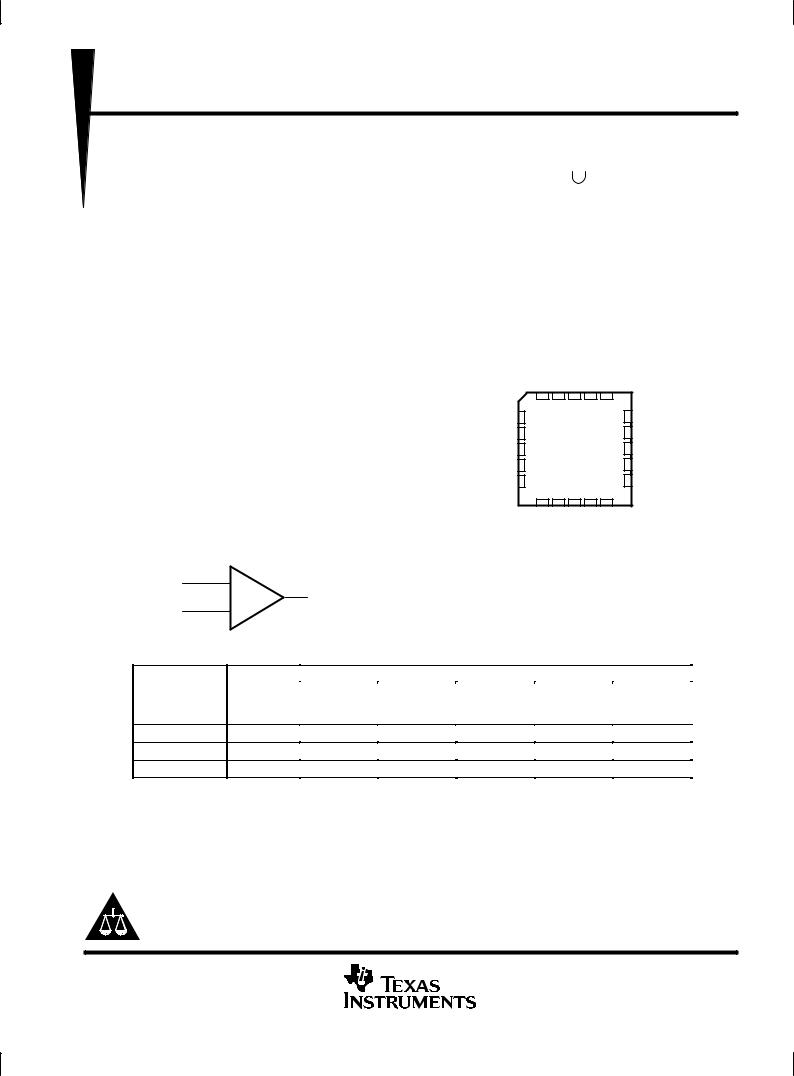
LM148 . . . J PACKAGE
LM248, LM348 . . . D, N, OR PW PACKAGE
(TOP VIEW)
1OUT |
|
1 |
14 |
|
4OUT |
|
|
||||
1IN ± |
|
2 |
13 |
|
4IN± |
|
|
||||
1 IN+ |
|
3 |
12 |
|
4IN+ |
|
|
||||
VCC + |
|
4 |
11 |
|
VCC ± |
|
|
||||
|
|
||||
2IN + |
|
5 |
10 |
|
3IN+ |
2IN± |
|
6 |
9 |
|
3IN± |
|
|
||||
2OUT |
|
7 |
8 |
|
3OUT |
|
|
||||
|
|
|
|
|
|
description
LM148 . . . FK PACKAGE
The LM148, LM248, and LM348 are quadruple, independent, high-gain, internally compensated operational amplifiers designed to have operating characteristics similar to the μA741. These amplifiers exhibit low supply current drain, and input bias and offset currents that are much less than those of the μA741.
The LM148 is characterized for operation over the full military temperature range of ±55°C to 125°C, the LM248 is characterized for operation from ±25°C to 85°C, and the LM348 is characterized for operation from 0°C to 70°C.
symbol (each amplifier)
(TOP VIEW)
|
1IN ± |
1OUT |
NC |
4OUT |
4IN ± |
|
1IN+ |
3 |
2 |
1 |
20 19 |
4IN+ |
|
4 |
|
|
|
18 |
||
NC |
5 |
|
|
|
17 |
NC |
VCC + |
6 |
|
|
|
16 |
VCC ± |
NC |
7 |
|
|
|
15 |
NC |
2IN+ |
8 |
|
|
|
14 |
3IN+ |
|
9 |
10 11 12 13 |
|
|||
|
2IN ± |
2OUT |
NC |
3OUT |
3IN ± |
|
IN +
NC ± No internal connection
+
OUT
IN ±
TA
0°C to 70°C
±25°C to 85°C
±55°C to 125°C
±
AVAILABLE OPTIONS
|
|
|
PACKAGE |
|
|
|
VIOmax |
|
|
|
|
|
|
SMALL |
CHIP |
CERAMIC |
PLASTIC |
TSSOP |
||
AT 25°C |
OUTLINE |
CARRIER |
DIP |
DIP |
||
(PW) |
||||||
|
(D) |
(FK) |
(J) |
(N) |
||
|
|
|||||
6 mV |
LM348D |
Ð |
Ð |
LM348N |
LM348PW |
|
6 mV |
LM248D |
Ð |
Ð |
LM248N |
Ð |
|
5 mV |
Ð |
LM148FK |
LM148J |
Ð |
Ð |
|
|
|
|
|
|
|
The D package is available taped and reeled. Add the suffix R to the device type (e.g., LM348DR).
Please be aware that an important notice concerning availability, standard warranty, and use in critical applications of Texas Instruments semiconductor products and disclaimers thereto appears at the end of this data sheet.
PRODUCTION DATA information is current as of publication date. Products conform to specifications per the terms of Texas Instruments standard warranty. Production processing does not necessarily include testing of all parameters.
Copyright 1996, Texas Instruments Incorporated
POST OFFICE BOX 655303 •DALLAS, TEXAS 75265 |
1 |

LM148, LM248, LM348
QUADRUPLE OPERATIONAL AMPLIFIERS
SLOS058B ± OCTOBER 1979 ± REVISED AUGUST 1996
absolute maximum ratings over operating free-air temperature range (unless otherwise noted)
|
|
LM148 |
LM248 |
LM348 |
UNIT |
|
|
|
|
|
|
Supply voltage, VCC+ (see Note 1) |
|
22 |
18 |
18 |
V |
Supply voltage, VCC ± (see Note 1) |
|
± 22 |
± 18 |
± 18 |
V |
Differential input voltage, VID (see Note 2) |
|
44 |
36 |
36 |
V |
Input voltage, VI (either input, see Notes 1 and 3) |
|
± 22 |
± 18 |
± 18 |
V |
Duration of output short circuit (see Note 4) |
|
unlimited |
unlimited |
unlimited |
|
|
|
|
|
|
|
Continuous total power dissipation |
|
See Dissipation Rating Table |
|
||
|
|
|
|
|
|
Operating free-air temperature range, TA |
|
± 55 to 125 |
± 25 to 85 |
0 to 70 |
°C |
Storage temperature range |
|
± 65 to 150 |
± 65 to 150 |
± 65 to 150 |
°C |
|
|
|
|
|
|
Case temperature for 60 seconds |
FK package |
260 |
|
|
°C |
|
|
|
|
|
|
Lead temperature 1,6 mm (1/16 inch) from case for 60 seconds |
J package |
300 |
|
|
°C |
|
|
|
|
|
|
Lead temperature 1,6 mm (1/16 inch) from case for 10 seconds |
D, N, or PW package |
|
260 |
260 |
°C |
|
|
|
|
|
|
NOTES: 1. All voltage values, except differential voltages, are with respect to the midpoint between VCC + and VCC ±.
2.Differential voltages are at IN+ with respect to IN ±.
3.The magnitude of the input voltage must never exceed the magnitude of the supply voltage or the value specified in the table, whichever is less.
4.The output may be shorted to ground or either power supply. Temperature and/or supply voltages must be limited to ensure that the dissipation rating is not exceeded.
DISSIPATION RATING TABLE
PACKAGE |
TA ≤ 25°C |
DERATING |
DERATE |
TA = 70°C |
TA = 85°C |
TA = 125°C |
|
POWER RATING |
FACTOR |
ABOVE TA |
POWER RATING |
POWER RATING |
POWER RATING |
||
|
|||||||
D |
900 mW |
7.6 mW/°C |
32°C |
611 mW |
497 mW |
N/A |
|
FK |
900 mW |
11.0 mW/°C |
68°C |
878 mW |
713 mW |
273 mW |
|
J |
900 mW |
11.0 mW/°C |
68°C |
878 mW |
713 mW |
273 mW |
|
N |
900 mW |
9.2 mW/°C |
52°C |
734 mW |
596 mW |
N/A |
|
PW |
700 mW |
5.6 mW/°C |
N/A |
448 mW |
N/A |
N/A |
|
|
|
|
|
|
|
|
recommended operating conditions
|
MIN |
MAX |
UNIT |
|
|
|
|
Supply voltage, VCC + |
4 |
18 |
V |
Supply voltage, VCC ± |
± 4 |
± 18 |
V |
2 |
POST OFFICE BOX 655303 •DALLAS, TEXAS 75265 |
 Loading...