


 Loading...
LM3445
www.ti.com |
SNVS570L –JANUARY 2009 –REVISED MAY 2013 |
Triac Dimmable Offline LED Driver
Check for Samples: LM3445
FEATURES
•Triac Dim Decoder Circuit for LED Dimming
•Application Voltage Range 80VAC – 277VAC
•Capable of Controlling LED Currents Greater Than 1A
•Adjustable Switching Frequency
•Low Quiescent Current
•Adaptive Programmable Off-Time Allows for Constant Ripple Current
•Thermal Shutdown
•No 120Hz Flicker
•Low Profile 10-Pin VSSOP Package or 14-Pin SOIC
•Patent Pending Drive Architecture
DESCRIPTION
The LM3445 is an adaptive constant off-time AC/DC buck (step-down) constant current controller designed to be compatible with triac dimmers. The LM3445 provides a constant current for illuminating high power LEDs and includes a triac dim decoder. The dim decoder allows wide range LED dimming using standard triac dimmers. The high frequency capable architecture allows the use of small external passive components. The LM3445 includes a bleeder circuit to ensure proper triac operation by allowing current flow while the line voltage is low to enable proper firing of the triac. A passive PFC circuit ensures good power factor by drawing current directly from the line for most of the cycle, and provides a constant positive voltage to the buck regulator. Additional features include thermal shutdown, current limit and VCC under-voltage lockout.
APPLICATIONS
•Retro Fit Triac Dimming
•Solid State Lighting
•Industrial and Commercial Lighting
•Residential Lighting
Typical LM3445 LED Driver Application Circuit
|
V+ |
|
D3 |
|
|
|
VBUCK |
|
|
|
|
|
C7 |
+ |
D9 |
|
|
|
|
BR1 |
|
|
|
|
D8 |
|
C10 |
VLED |
|
|
|
|
|
|
+ |
|
|
||
|
|
R2 |
D4 |
|
C9 |
C12 |
- |
R4 |
|
TRIAC |
|
|
Q1 |
|
D2 |
|
VLED- |
|
|
DIMMER |
|
|
|
|
|
|
|
||
|
|
|
|
|
|
|
|
||
VAC |
|
|
|
|
|
|
|
|
|
|
|
D1 |
R5 |
|
|
|
D10 |
|
|
|
|
|
|
|
C5 |
|
|
|
Q3 |
|
|
|
|
|
|
|
|
L2 |
|
|
LM3445MM |
|
|
|
|
|
|
||
1 |
ASNS |
U1 |
BLDR 10 |
|
|
|
|
|
|
|
|
|
|
|
|
|
|
|
|
R1 |
|
|
ICOLL |
2 |
FLTR1 |
VCC 9 |
|
C3 |
|
|
|
3 |
DIM |
GATE 8 |
Q2 |
4 |
COFF |
ISNS 7 |
|
5 |
FLTR2 |
GND 6 |
R3 |
|
|||
C4 |
|
|
|
C11 
EFFICIENCY (%)
95.0
14 Series connected LEDs
90.0
85.0
10 Series connected LEDs
80.0
75.0
80 |
90 |
100 |
110 |
120 |
130 |
140 |
|
|
LINE VOLTAGE (VAC) |
|
|
||
Please be aware that an important notice concerning availability, standard warranty, and use in critical applications of
Texas Instruments semiconductor products and disclaimers thereto appears at the end of this data sheet.
All trademarks are the property of their respective owners.
PRODUCTION DATA information is current as of publication date. |
Copyright © 2009–2013, Texas Instruments Incorporated |
Products conform to specifications per the terms of the Texas |
|
Instruments standard warranty. Production processing does not |
|
necessarily include testing of all parameters. |
|

LM3445
SNVS570L –JANUARY 2009–REVISED MAY 2013 www.ti.com
|
DEVICE INFORMATION |
|
ORDER NUMBER(1) |
|
TOP MARK |
LM3445M/NOPB |
|
SULB |
|
|
|
LM3445MM/NOPB |
|
SULB |
|
|
|
LM3445MMX/NOPB |
|
LM3445M |
|
|
|
LM3445MX/NOPB |
|
LM3445M |
|
|
|
(1)For the most current package and ordering information, see the Package Option Addendum at the end of this document, or see the TI web site at www.ti.com.
Connection Diagram
|
|
Top View |
|
|
|
Top View |
|
||
ASNS |
1 |
|
10 |
BLDR |
COFF |
1 |
|
14 |
DIM |
|
|
||||||||
FLTR1 |
2 |
|
9 |
VCC |
N/C |
2 |
|
13 |
FLTR1 |
DIM |
3 |
|
8 |
GATE |
FLTR2 |
3 |
|
12 |
ASNS |
COFF |
4 |
|
7 |
ISNS |
GND |
4 |
|
11 |
N/C |
FLTR2 |
5 |
|
6 |
GND |
N/C |
5 |
|
10 |
BLDR |
|
|
|
|
|
|
|
|
9 |
VCC |
|
|
|
|
|
|
|
|
||
|
|
|
|
|
N/C |
6 |
|
||
|
|
|
|
|
|
|
|
8 |
GATE |
|
|
|
|
|
ISNS |
7 |
|
||
|
|
|
|
|
|
|
|
|
|
|
|
|
|
|
|
|
|
|
|
|
Figure 1. 10-Pin VSSOP |
Figure 2. 14-Pin SOIC |
||
|
Package Number DGS |
Package Number D |
||
|
|
|
PIN DESCRIPTIONS |
|
|
|
|
|
|
SOIC |
VSSOP |
Name |
Description |
|
|
|
|
|
|
12 |
1 |
ASNS |
PWM output of the triac dim decoder circuit. Outputs a 0 to 4V PWM signal with a duty cycle |
|
|
|
|
proportional to the triac dimmer on-time. |
|
|
|
|
|
|
13 |
2 |
FLTR1 |
First filter input. The 120Hz PWM signal from ASNS is filtered to a DC signal and compared to a 1 to |
|
|
|
|
3V, 5.85 kHz ramp to generate a higher frequency PWM signal with a duty cycle proportional to the |
|
|
|
|
triac dimmer firing angle. Pull above 4.9V (typical) to tri-state DIM. |
|
14 |
3 |
DIM |
Input/output dual function dim pin. This pin can be driven with an external PWM signal to dim the |
|
|
|
|
LEDs. It may also be used as an output signal and connected to the DIM pin of other LM3445s or |
|
|
|
|
other LED drivers to dim multiple LED circuits simultaneously. |
|
|
|
|
|
|
1 |
4 |
COFF |
OFF time setting pin. A user set current and capacitor connected from the output to this pin sets the |
|
|
|
|
constant OFF time of the switching controller. |
|
|
|
|
|
|
3 |
5 |
FLTR2 |
Second filter input. A capacitor tied to this pin filters the PWM dimming signal to supply a DC voltage |
|
|
|
|
to control the LED current. Could also be used as an analog dimming input. |
|
|
|
|
|
|
4 |
6 |
GND |
Circuit ground connection. |
|
|
|
|
|
|
7 |
7 |
ISNS |
LED current sense pin. Connect a resistor from main switching MOSFET source, ISNS to GND to set |
|
|
|
|
the maximum LED current. |
|
8 |
8 |
GATE |
Power MOSFET driver pin. This output provides the gate drive for the power switching MOSFET of the |
|
|
|
|
buck controller. |
|
|
|
|
|
|
9 |
9 |
VCC |
Input voltage pin. This pin provides the power for the internal control circuitry and gate driver. |
|
10 |
10 |
BLDR |
Bleeder pin. Provides the input signal to the angle detect circuitry as well as a current path through a |
|
|
|
|
switched 230Ω resistor to ensure proper firing of the triac dimmer. |
|
2,5,6,11 |
- |
N/C |
No Connect |
|
|
|
|
|
|
2 |
Submit Documentation Feedback |
Copyright © 2009–2013, Texas Instruments Incorporated |
Product Folder Links: LM3445

LM3445
www.ti.com |
SNVS570L –JANUARY 2009 –REVISED MAY 2013 |
These devices have limited built-in ESD protection. The leads should be shorted together or the device placed in conductive foam during storage or handling to prevent electrostatic damage to the MOS gates.
ABSOLUTE MAXIMUM RATINGS (1) (2)
BLDR to GND |
-0.3V to +17V |
|
|
VCC, GATE, FLTR1 to GND |
-0.3V to +14V |
ISNS to GND |
-0.3V to +2.5V |
|
|
ASNS, DIM, FLTR2, COFF to GND |
-0.3V to +7.0V |
|
|
COFF Input Current |
100mA |
|
|
Continuous Power Dissipation(3) |
Internally Limited |
ESD Susceptibility, HBM (4) |
2 kV |
Junction Temperature (TJ-MAX) |
150°C |
Storage Temperature Range |
-65°C to +150°C |
|
|
Maximum Lead Temperature Range (Soldering) |
260°C |
|
|
(1)Absolute maximum ratings are limits beyond which damage to the device may occur. Operating Ratings are conditions for which the device is intended to be functional, but device parameter specifications may not be guaranteed. For ensured specifications and test conditions, see the Electrical Characteristics. All voltages are with respect to the potential at the GND pin, unless otherwise specified.
(2)If Military/Aerospace specified devices are required, please contact the Texas Instruments Sales Office/Distributors for availability and specifications.
(3)Internal thermal shutdown circuitry protects the device from permanent damage. Thermal shutdown engages at TJ = 165°C (typ.) and disengages at TJ = 145°C (typ).
(4)Human Body Model, applicable std. JESD22-A114-C.
OPERATING CONDITIONS
VCC |
8.0V to 12V |
Junction Temperature |
−40°C to +125°C |
ELECTRICAL CHARACTERISTICS
Limits in standard type face are for TJ = 25°C and those with boldface type apply over the full Operating Temperature Range ( TJ = −40°C to +125°C). Minimum and Maximum limits are specified through test, design, or statistical correlation. Typical values represent the most likely parametric norm at TJ = +25ºC, and are provided for reference purposes only.
Symbol |
Parameter |
Conditions |
Min |
Typ |
Max |
Units |
|
|
|
|
|
|
|
BLEEDER |
|
|
|
|
|
|
|
|
|
|
|
|
|
RBLDR |
Bleeder resistance to GND |
IBLDR = 10mA |
|
230 |
325 |
Ω |
VCC SUPPLY |
|
|
|
|
|
|
IVCC |
Operating supply current |
|
|
2.00 |
2.85 |
mA |
VCC-UVLO |
Rising threshold |
|
|
7.4 |
7.7 |
V |
|
Falling threshold |
|
6.0 |
6.4 |
|
|
|
|
|
|
|
|
|
|
Hysterisis |
|
|
1 |
|
|
|
|
|
|
|
|
|
COFF |
|
|
|
|
|
|
|
|
|
|
|
|
|
VCOFF |
Time out threshold |
|
1.225 |
1.276 |
1.327 |
V |
RCOFF |
Off timer sinking impedance |
|
|
33 |
60 |
Ω |
tCOFF |
Restart timer |
|
|
180 |
|
µs |
CURRENT LIMIT |
|
|
|
|
|
|
|
|
|
|
|
|
|
VISNS |
ISNS limit threshold |
|
1.174 |
1.269 |
1.364 |
V |
tISNS |
Leading edge blanking time |
|
|
125 |
|
ns |
|
Current limit reset delay |
|
|
180 |
|
µs |
|
|
|
|
|
|
|
|
ISNS limit to GATE delay |
ISNS = 0 to 1.75V step |
|
33 |
|
ns |
|
|
|
|
|
|
|
Copyright © 2009–2013, Texas Instruments Incorporated |
Submit Documentation Feedback |
3 |
Product Folder Links: LM3445

LM3445
SNVS570L –JANUARY 2009–REVISED MAY 2013 |
www.ti.com |
ELECTRICAL CHARACTERISTICS (continued)
Limits in standard type face are for TJ = 25°C and those with boldface type apply over the full Operating Temperature Range ( TJ = −40°C to +125°C). Minimum and Maximum limits are specified through test, design, or statistical correlation. Typical values represent the most likely parametric norm at TJ = +25ºC, and are provided for reference purposes only.
Symbol |
Parameter |
Conditions |
Min |
Typ |
Max |
Units |
|
|
|
|
|
|
|
INTERNAL PWM RAMP |
|
|
|
|
|
|
|
|
|
|
|
|
|
fRAMP |
Frequency |
|
|
5.85 |
|
kHz |
VRAMP |
Valley voltage |
|
0.96 |
1.00 |
1.04 |
V |
|
Peak voltage |
|
2.85 |
3.00 |
3.08 |
|
|
|
|
|
|
|
|
DRAMP |
Maximum duty cycle |
|
96.5 |
98.0 |
|
% |
DIM DECODER |
|
|
|
|
|
|
|
|
|
|
|
|
|
tANG_DET |
Angle detect rising threshold |
Observed on BLDR pin |
6.79 |
7.21 |
7.81 |
V |
VASNS |
ASNS filter delay |
|
|
4 |
|
µs |
|
ASNS VMAX |
|
3.85 |
4.00 |
4.15 |
V |
|
|
|
|
|
|
|
IASNS |
ASNS drive capability sink |
VASNS = 2V |
|
7.6 |
|
mA |
|
ASNS drive capability source |
VASNS = 2V |
|
-4.3 |
|
|
|
DIM low sink current |
VDIM = 1V |
1.65 |
2.80 |
|
|
|
DIM High source current |
VDIM = 4V |
|
-4.00 |
-3.00 |
|
VDIM |
DIM low voltage |
PWM input voltage |
0.9 |
1.33 |
|
V |
|
|
threshold |
|
|
|
|
|
DIM high voltage |
|
|
2.33 |
3.15 |
|
|
|
|
|
|
|
|
VTSTH |
Tri-state threshold voltage |
Apply to FLTR1 pin |
|
4.87 |
5.25 |
V |
RDIM |
DIM comparator tri-state impedance |
|
10 |
|
|
MΩ |
CURRENT SENSE COMPARATOR |
|
|
|
|
|
|
|
|
|
|
|
|
|
VFLTR2 |
FLTR2 open circuit voltage |
|
720 |
750 |
780 |
mV |
RFLTR2 |
FLTR2 impedance |
|
|
420 |
|
kΩ |
VOS |
Current sense comparator offset voltage |
|
-4.0 |
0.1 |
4.0 |
mV |
GATE DRIVE OUTPUT |
|
|
|
|
|
|
|
|
|
|
|
|
|
VDRVH |
GATE high saturation |
IGATE = 50 mA |
|
0.24 |
0.50 |
V |
VDRVL |
GATE low saturation |
IGATE = 100 mA |
|
0.22 |
0.50 |
|
IDRV |
Peak souce current |
GATE = VCC/2 |
|
-0.77 |
|
A |
|
Peak sink current |
GATE = VCC/2 |
|
0.88 |
|
|
tDV |
Rise time |
Cload = 1 nF |
|
15 |
|
ns |
|
Fall time |
Cload = 1 nF |
|
15 |
|
|
THERMAL SHUTDOWN |
|
|
|
|
|
|
|
|
|
|
|
|
|
T |
Thermal shutdown temperature |
See (1) |
|
165 |
|
°C |
SD |
|
|
|
|
|
|
|
Thermal shutdown hysteresis |
|
|
20 |
|
|
|
|
|
|
|
|
|
THERMAL SHUTDOWN |
|
|
|
|
|
|
|
|
|
|
|
|
|
RθJA |
VSSOP-10 junction to ambient |
|
|
121 |
|
°C/W |
(1)Junction-to-ambient thermal resistance is highly application and board-layout dependent. In applications where high maximum power dissipation exists, special care must be paid to thermal dissipation issues in board design. In applications where high power dissipation and/or poor package thermal resistance is present, the maximum ambient temperature may have to be derated. Maximum ambient
temperature (TA-MAX) is dependent on the maximum operating junction temperature (TJ-MAX-OP = 125°C), the maximum power dissipation of the device in the application (PD-MAX), and the junction-to ambient thermal resistance of the part/package in the application (RθJA), as given by the following equation: TA-MAX = TJ-MAX-OP – (RθJA × PD-MAX).
4 |
Submit Documentation Feedback |
Copyright © 2009–2013, Texas Instruments Incorporated |
Product Folder Links: LM3445

LM3445
www.ti.com |
SNVS570L –JANUARY 2009 –REVISED MAY 2013 |
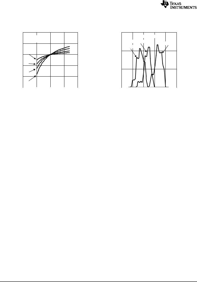
TYPICAL PERFORMANCE CHARACTERISTICS
fSW vs Input Line Voltage
300k
250k
7 LEDs in Series (VO = 24.5V)
(Hz) |
200k |
|
|
|
|
|
|
|
|
|
|
|
|
|
|
|
|
|
|
|
|
|
|
|
|
|
|
|
|
||
|
|
|
|
|
|
|
|
|
|
|
|
|
|
|
|
SW |
150k |
|
|
|
|
|
|
|
|
|
|
|
|
|
|
|
|
|
|
|
|
|
|
|
|
|
|
|
|
|
|
f |
|
|
|
|
|
|
|
|
|
|
|
|
|
|
|
|
100k |
|
|
|
|
|
|
|
|
|
|
|
|
|
|
|
|
|
|
|
|
|
|
|
|
|
|
|
|
|
|
|
50k |
|
|
|
|
|
|
|
|
|
|
|
|
|
|
|
|
|
|
|
|
|
|
|
|
|
|
|
|
|
|
|
|
|
|
|
|
C11 = |
2.2 nF, |
R3 = 348 k: |
|
||||||
|
0 |
|
|
|
|
|
|
|
|
|
|
|
|
|
|
|
|
|
|
|
|
|
|
|
|
|
|
|
|
|
|
|
80 |
90 |
100 |
110 |
120 |
130 |
140 |
||||||||
LINE VOLTAGE (VAC)
Figure 3.
BLDR Resistor vs Temperature
|
300 |
|
|
280 |
|
(Ö) |
260 |
|
RESISTORBLDR |
||
240 |
||
|
||
|
220 |
|
|
200 |
-50 -25 0 25 50 75 100 125 150 TEMPERATURE (°C)
Figure 5.
EFFICIENCY (%)
UVLO (V)
Efficiency vs Input Line Voltage
95.0
14 Series connected LEDs
90.0
85.0
10 Series connected LEDs
80.0
75.0
80 |
90 |
100 |
110 |
120 |
130 |
140 |
|
|
LINE VOLTAGE (VAC) |
|
|
||
Figure 4.
VCC UVLO vs Temperature
8.0
UVLO (VCC) Rising
7.5
7.0
UVLO (VCC) Falling
6.5
6.0 -50 -25 0 25 50 75 100 125 150
TEMPERATURE (°C)
Figure 6.
tON-MIN (ns)
Min On-Time (tON) vs Temperature
200.0
190.0
180.0
170.0
160.0
150.0 -50 -25 0 25 50 75 100 125 150
TEMPERATURE (°C)
Figure 7.
Off Threshold (C11) vs Temperature
|
1.29 |
|
|
1.28 |
|
(V) |
1.27 |
|
OFF |
||
|
||
V |
OFF Threshold at C11 |
|
|
1.26
1.25 -50 -25 0 25 50 75 100 125 150
TEMPERATURE (°C)
Figure 8.
Copyright © 2009–2013, Texas Instruments Incorporated |
Submit Documentation Feedback |
5 |
Product Folder Links: LM3445
LM3445
SNVS570L –JANUARY 2009–REVISED MAY 2013 |
www.ti.com |
TYPICAL PERFORMANCE CHARACTERISTICS (continued)
NORMALIZED SW FREQ
Normalized Variation in fSW over VBUCK Voltage
1.50
Series connected LEDs
1.25
3 LEDs
1.00
5 LEDs
0.75
7 LEDs
0.50
9 LEDs
0.25
0 50 100 150 200
VBUCK (V)
Figure 9.
NUMBER OF UNITS
Leading Edge Blanking Variation Over Temperature
15.0
100 units tested
Room (25°C)
Hot (125°C)
Cold (-40°C)
10.0
5.0
0.0 |
|
|
|
|
|
80 |
100 |
120 |
140 |
160 |
180 |
LEADING EDGE BLANKING (ns)
Figure 10.
6 |
Submit Documentation Feedback |
Copyright © 2009–2013, Texas Instruments Incorporated |
Product Folder Links: LM3445
LM3445
www.ti.com |
SNVS570L –JANUARY 2009 –REVISED MAY 2013 |
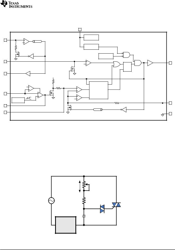
SIMPLIFIED INTERNAL BLOCK DIAGRAM
|
|
|
|
VCC |
|
|
BLDR |
|
ANGLE DETECT |
|
INTERNAL |
|
LM3445 |
|
|
|
REGULATORS |
|
||
|
7.2V |
4 Ps |
|
|
|
|
|
|
|
|
|
|
|
|
230 |
|
|
VCC UVLO |
|
|
|
BLEEDER |
|
|
|
|
|
|
|
|
|
THERMAL |
|
MOSFET |
COFF |
|
|
|
SHUTDOWN |
|
DRIVER |
|
|
|
COFF |
|
GATE |
|
|
|
|
|
|
|
|
|
|
|
33: |
1.276V |
S |
Q |
|
|
|
|
START |
|
|
ASNS |
|
|
|
|
R |
|
0V to 4V |
|
|
|
|
|
|
|
|
|
|
LATCH |
||
|
|
|
|
|
||
|
|
|
750 mV |
|
|
|
|
|
DIM DECODER |
50k |
|
|
|
|
4.9V |
Tri-State |
370k |
PWM |
|
|
|
|
|
|
|
|
|
FLTR1 |
|
|
RAMP |
CONTROLLER |
|
|
|
|
|
I-LIM |
|
|
|
|
|
|
|
|
|
|
|
RAMP GEN. |
3V |
1.27V |
|
|
|
|
1V |
1k |
|
ISNS |
||
DIM |
5.9 kHz |
|
|
|
||
|
|
|
|
|
||
|
|
|
|
|
|
|
|
|
|
|
LEADING EDGE BLANKING |
|
|
FLTR2 |
|
|
|
125 ns |
|
GND |
|
|
|
|
|
|
|
Figure 11. Simplified Block Diagram
APPLICATION INFORMATION
FUNCTIONAL DESCRIPTION
The LM3445 contains all the necessary circuitry to build a line-powered (mains powered) constant current LED driver whose output current can be controlled with a conventional triac dimmer.
OVERVIEW OF PHASE CONTROL DIMMING
A basic "phase controlled" triac dimmer circuit is shown in Figure 12.
BRIGHT |
R1 250 KÖ |
DIM |
|
|
TRIAC |
MAINS AC |
R2 3.3 KÖ |
DIAC |
C1 100 NF |
LOAD |
Figure 12. Basic Triac Dimmer
Copyright © 2009–2013, Texas Instruments Incorporated |
Submit Documentation Feedback |
7 |
Product Folder Links: LM3445
LM3445
SNVS570L –JANUARY 2009–REVISED MAY 2013 |
www.ti.com |
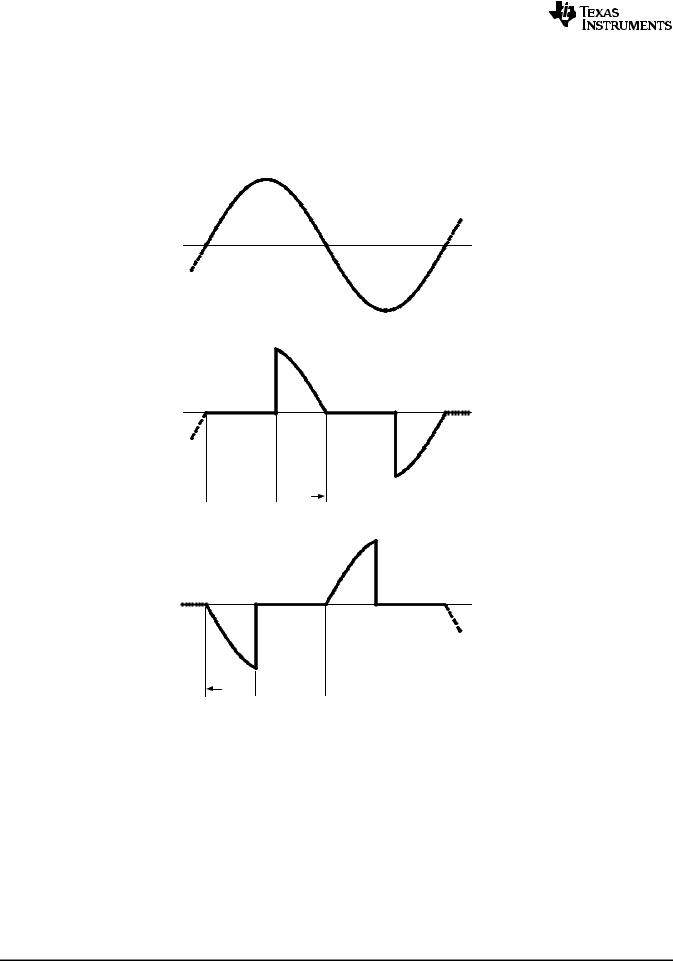
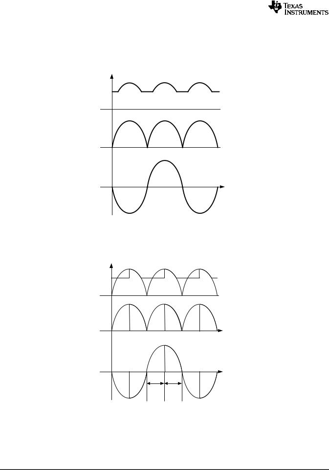
An RC network consisting of R1, R2, and C1 delay the turn on of the triac until the voltage on C1 reaches the trigger voltage of the diac. Increasing the resistance of the potentiometer (wiper moving downward) increases the turn-on delay which decreases the on-time or "conduction angle" of the triac (θ). This reduces the average power delivered to the load. Voltage waveforms for a simple triac dimmer are shown in Figure 13. Figure 13a shows the full sinusoid of the input voltage. Even when set to full brightness, few dimmers will provide 100% on-time, i.e., the full sinusoid.
(a)
(b) |
 DELAY
DELAY 
 ?
?
(c) |
? 
 DELAY
DELAY
Figure 13. Line Voltage and Dimming Waveforms
Figure 13b shows a theoretical waveform from a dimmer. The on-time is often referred to as the "conduction angle" and may be stated in degrees or radians. The off-time represents the delay caused by the RC circuit feeding the triac. The off-time be referred to as the "firing angle" and is simply 180° - θ.
Figure 13c shows a waveform from a so-called reverse phase dimmer, sometimes referred to as an electronic dimmer. These typically are more expensive, microcontroller based dimmers that use switching elements other than triacs. Note that the conduction starts from the zero-crossing, and terminates some time later. This method of control reduces the noise spike at the transition.
Since the LM3445 has been designed to assess the relative on-time and control the LED current accordingly, most phase-control dimmers, both forward and reverse phase, may be used with success.
8 |
Submit Documentation Feedback |
Copyright © 2009–2013, Texas Instruments Incorporated |
Product Folder Links: LM3445
LM3445
www.ti.com |
SNVS570L –JANUARY 2009 –REVISED MAY 2013 |
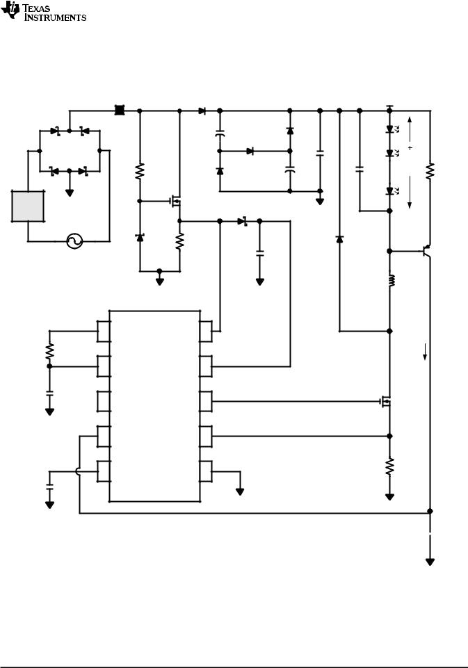
THEORY OF OPERATION
Refer to Figure 14 which shows the LM3445 along with basic external circuitry.
V+ |
D3 |
|
VBUCK |
|
|
|
|
C7 + |
D9 |
|
|
|
|
BR1 |
D8 |
|
C10 |
VLED |
|
|
R2 |
C9 + |
C12 |
R4 |
|||
D4 |
- |
TRIAC |
Q1 |
D2 |
VLED- |
DIMMER |
|
||
|
|
VAC
D1 |
R5 |
D10 |
|
C5 |
Q3 |
L2
|
LM3445MM |
||
1 |
ASNS |
U1 |
BLDR 10 |
|
|
|
|
R1 |
ICOLL |
2 |
FLTR1 |
VCC 9 |
C3 |
|
|
|
3 |
DIM |
GATE 8 |
Q2 |
4 |
COFF |
ISNS 7 |
5 FLTR2 |
GND 6 |
R3 |
|
||
C4 |
|
|
C11 
Figure 14. LM3445 Schematic
Copyright © 2009–2013, Texas Instruments Incorporated |
Submit Documentation Feedback |
9 |
Product Folder Links: LM3445
LM3445
SNVS570L –JANUARY 2009–REVISED MAY 2013 |
www.ti.com |
SENSING THE RECTIFIED TRIAC WAVEFORM
A bridge rectifier, BR1, converts the line (mains) voltage (Figure 15c) into a series of half-sines as shown in Figure 15b. Figure 15a shows a typical voltage waveform after diode D3 (valley fill circuit, or VBUCK).
VBUCK
 (a)
(a)
VBR1
 (b)
(b)
VAC
(c)
t
Figure 15. Voltage Waveforms After Bridge Rectifier Without Triac Dimming
Figure 16c and Figure 16b show typical triac dimmed voltage waveforms before and after the bridge rectifier. Figure 16a shows a typical triac dimmed voltage waveform after diode D3 (valley fill circuit, or VBUCK).
VBUCK
 (a) t
(a) t
VBR1
(b)
t
VAC
(c)
t
delay ?
Figure 16. Voltage Waveforms After Bridge Rectifier With Triac Dimming
LM3445 LINE SENSING CIRCUITRY
An external series pass regulator (R2, D1, and Q1) translates the rectified line voltage to a level where it can be sensed by the BLDR pin on the LM3445.
10 |
Submit Documentation Feedback |
Copyright © 2009–2013, Texas Instruments Incorporated |
Product Folder Links: LM3445
LM3445
www.ti.com |
SNVS570L –JANUARY 2009 –REVISED MAY 2013 |
V+
R2 |
|
|
Q1 |
|
D2 |
D1 |
|
R5 |
C5 |
|
R11 |
|
|
|
|
|
|
|
|
|
|
|
|
LM3445MM |
|
|
|
|
|
|
|
|
|
|
|
|
|
|
|
|
|
|
|
|
|
|
|
|
|
|
|
|
|
|
|
|
|
|
U1 |
|
|
|
|
|
|
|
|
|
|
|
|
|
|
1 |
ASNS |
BLDR |
10 |
|
|
|
|
|
|
|
|
|
|
|
|
|
|
|
|
|
|
|
R1 |
|
|
|
|
|
|
||||||||||
C3 |
|
|
|
|
|
|
|
|
|
|
2 |
FLTR1 |
VCC |
9 |
|
|
|
|
|
|
|
|
|
|
|
|
|
|
|||||
|
|
|
|
|
|
|
|
|
|
|
|
|||||
|
|
|
|
|
|
|
|
|
|
|
|
|
|
|
|
|
|
|
|
|
|
|
|
|
|
|
|
|
|
|
|||
|
|
|
|
|
|
|
|
|
|
|
|
|
|
|
|
|
|
|
|
|
|
|
|
|
|
|
|
3 |
DIM |
GATE |
8 |
|
|
|
|
|
|
|
|
|
|
|
|
|
|
|
|
|
|
|
|
|
|
|
|
|
|
|
|
|
|
|
|
|
|
|
|
|
4 |
COFF |
ISNS |
7 |
|
|
||||||||||
|
|
|
|
|
|
|
|
|
|
|
|
|
|
|
|
|
|
|
|
|
|
|
|
|
|
|
|
|
|
|
|
|
|
C4 |
|
|
|
|
5 |
FLTR2 |
GND |
6 |
|
|
||||||
|
|
|
|
|
|
|
|
|
|
|||||||
|
|
|
|
|
|
|
|
|
||||||||
|
|
|
|
|
|
|
|
|
|
|
|
|
|
|
|
|
Figure 17. LM3445 AC Line Sense Circuitry
D1 is typically a 15V zener diode which forces transistor Q1 to “stand-off” most of the rectified line voltage. Having no capacitance on the source of Q1 allows the voltage on the BLDR pin to rise and fall with the rectified line voltage as the line voltage drops below zener voltage D1 (see ANGLE DETECT).
A diode-capacitor network (D2, C5) is used to maintain the voltage on the VCC pin while the voltage on the BLDR pin goes low. This provides the supply voltage to operate the LM3445.
Resistor R5 is used to bleed charge out of any stray capacitance on the BLDR node and may be used to provide the necessary holding current for the dimmer when operating at light output currents.
TRIAC HOLDING CURRENT RESISTOR
In order to emulate an incandescent light bulb (essentially a resistor) with any LED driver, the existing triac will require a small amount of holding current throughout the AC line cycle. An external resistor (R5) needs to be placed on the source of Q1 to GND to perform this function. Most existing triac dimmers only require a few milliamps of current to hold them on. A few “less expensive” triacs sold on the market will require a bit more current. The value of resistor R5 will depend on:
•What type of triac the LM3445 will be used with
•How many light fixtures are running off of the triac
With a single LM3445 circuit on a common triac dimmer, a holding current resistor between 3 kΩ and 5 kΩ will be required. As the number of LM3445 circuits is added to a single dimmer, the holding resistor R5’s resistance can be increased. A few triac dimmers will require a resistor as low as 1 kΩ or lower for a single LM3445 circuit. The trade-off will be performance vs efficiency. As the holding resistor R5 is increased, the overall efficiency per LM3445 will also increase.
Copyright © 2009–2013, Texas Instruments Incorporated |
Submit Documentation Feedback |
11 |
Product Folder Links: LM3445

LM3445
SNVS570L –JANUARY 2009–REVISED MAY 2013 |
www.ti.com |
ANGLE DETECT
The Angle Detect circuit uses a comparator with a fixed threshold voltage of 7.21V to monitor the BLDR pin to determine whether the triac is on or off. The output of the comparator drives the ASNS buffer and also controls the Bleeder circuit. A 4 µs delay line on the output is used to filter out noise that could be present on this signal.
The output of the Angle Detect circuit is limited to a 0V to 4.0V swing by the buffer and presented to the ASNS pin. R1 and C3 comprise a low-pass filter with a bandwidth on the order of 1.0Hz.
The Angle Detect circuit and its filter produce a DC level which corresponds to the duty cycle (relative on-time) of the triac dimmer. As a result, the LM3445 will work equally well with 50Hz or 60Hz line voltages.
BLEEDER
While the BLDR pin is below the 7.21V threshold, the bleeder MOSFET is on to place a small load (230Ω) on the series pass regulator. This additional load is necessary to complete the circuit through the triac dimmer so that the dimmer delay circuit can operate correctly. Above 7.21V, the bleeder resistor is removed to increase efficiency.
FLTR1 PIN
The FLTR1 pin has two functions. Normally, it is fed by ASNS through filter components R1 and C3 and drives the dim decoder. However, if the FLTR1 pin is tied above 4.9V (typical), e.g., to VCC, the Ramp Comparator is tri-stated, disabling the dim decoder. See MASTER/SLAVE OPERATION.
DIM DECODER
The ramp generator produces a 5.85 kHz saw tooth wave with a minimum of 1.0V and a maximum of 3.0V. The filtered ASNS signal enters pin FLTR1 where it is compared against the output of the Ramp Generator.
The output of the ramp comparator will have an on-time which is inversely proportional to the average voltage level at pin FLTR1. However, since the FLTR1 signal can vary between 0V and 4.0V (the limits of the ASNS pin), and the Ramp Generator signal only varies between 1.0V and 3.0V, the output of the ramp comparator will be on
continuously for VFLTR1 < 1.0V and off continuously for VFLTR1 > 3.0V. This allows a decoding range from 45° to 135° to provide a 0 – 100% dimming range.
The output of the ramp comparator drives both a common-source N-channel MOSFET through a Schmitt trigger and the DIM pin (see MASTER/SLAVE OPERATION for further functions of the DIM pin). The MOSFET drain is pulled up to 750 mV by a 50 kΩ resistor.
Since the MOSFET inverts the output of the ramp comparator, the drain voltage of the MOSFET is proportional to the duty cycle of the line voltage that comes through the triac dimmer. The amplitude of the ramp generator causes this proportionality to "hard limit" for duty cycles above 75% and below 25%.
The MOSFET drain signal next passes through an RC filter comprised of an internal 370 kΩ resistor, and an external capacitor on pin FLTR2. This forms a second low pass filter to further reduce the ripple in this signal, which is used as a reference by the PWM comparator. This RC filter is generally set to 10Hz.
The net effect is that the output of the dim decoder is a DC voltage whose amplitude varies from near 0V to 750 mV as the duty cycle of the dimmer varies from 25% to 75%. This corresponds to conduction angles of 45° to 135°, respectively.
The output voltage of the Dim Decoder directly controls the peak current that will be delivered by Q2 during its on-time. See BUCK CONVERTER for details.
As the triac fires beyond 135°, the DIM decoder no longer controls the dimming. At this point the LEDs will dim gradually for one of two reasons:
1.The voltage at VBUCK decreases and the buck converter runs out of headroom and causes LED current to decrease as VBUCK decreases.
2.Minimum on-time is reached which fixes the duty-cycle and therefore reduces the voltage at VBUCK.
The transition from dimming with the DIM decoder to headroom or minimum on-time dimming is seamless. LED currents from full load to as low as 0.5 mA can be easily achieved.
12 |
Submit Documentation Feedback |
Copyright © 2009–2013, Texas Instruments Incorporated |
Product Folder Links: LM3445
Loading...