


 Loading...
Texas Instruments LP2950ACZ, LP2951ACM, LP2951ACMM, LP2951ACSD, LP2951ACSDX Schematic [ru]
...LP2950-N, LP2951-N
www.ti.com |
SNVS764N –JANUARY 2000–REVISED MAY 2013 |
LP2950-N/LP2951-N Series of Adjustable Micropower Voltage Regulators
Check for Samples: LP2950-N, LP2951-N
FEATURES
•5V, 3V, and 3.3V Versions Available
•High Accuracy Output Voltage
•Ensured 100 mA Output Current
•Extremely Low Quiescent Current
•Low Dropout Voltage
•Extremely Tight Load and Line Regulation
•Very Low Temperature Coefficient
•Use as Regulator or Reference
•Needs Minimum Capacitance for Stability
•Current and Thermal Limiting
•Stable With Low-ESR Output Capacitors (10 mΩ to 6Ω)
LP2951-N VERSIONS ONLY
•Error Flag Warns of Output Dropout
•Logic-Controlled Electronic Shutdown
•Output Programmable From 1.24 to 29V
DESCRIPTION
The LP2950-N and LP2951-N are micropower voltage regulators with very low quiescent current (75 μA typ.) and very low dropout voltage (typ. 40 mV at light loads and 380 mV at 100 mA). They are ideally suited for use in battery-powered systems. Furthermore, the quiescent current of the LP2950- N/LP2951-N increases only slightly in dropout, prolonging battery life.
The LP2950-N-5.0 is available in the surface-mount PFM package, and in the popular 3-pin TO-92 package for pin-compatibility with older 5V regulators. The 8-lead LP2951-N is available in plastic, ceramic dual-in-line, WSON, or metal can packages and offers additional system functions.
One such feature is an error flag output which warns of a low output voltage, often due to falling batteries on the input. It may be used for a power-on reset. A second feature is the logic-compatible shutdown input which enables the regulator to be switched on and off. Also, the part may be pin-strapped for a 5V, 3V, or 3.3V output (depending on the version), or programmed from 1.24V to 29V with an external pair of resistors.
Careful design of the LP2950-N/LP2951-N has minimized all contributions to the error budget. This includes a tight initial tolerance (.5% typ.), extremely good load and line regulation (.05% typ.) and a very low output voltage temperature coefficient, making the part useful as a low-power voltage reference.
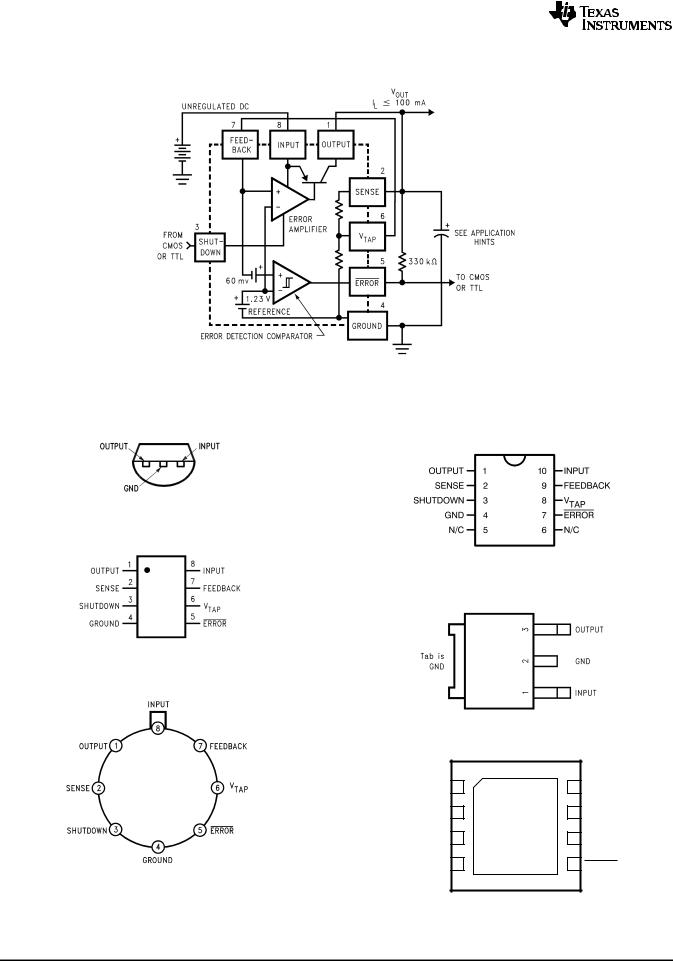
Block Diagram and Typical Applications
Figure 1. LP2950-N
Please be aware that an important notice concerning availability, standard warranty, and use in critical applications of
Texas Instruments semiconductor products and disclaimers thereto appears at the end of this data sheet.
All trademarks are the property of their respective owners.
PRODUCTION DATA information is current as of publication date. |
Copyright © 2000–2013, Texas Instruments Incorporated |
Products conform to specifications per the terms of the Texas |
|
Instruments standard warranty. Production processing does not |
|
necessarily include testing of all parameters. |
|
LP2950-N, LP2951-N
SNVS764N –JANUARY 2000 –REVISED MAY 2013 |
www.ti.com |
Figure 2. LP2951-N
Connection Diagrams
Figure 3. TO-92 Plastic Package (LP) Bottom
View
Figure 6. 10-Lead Ceramic Surface-Mount
Package (NAC) Top View
Figure 4. Dual-In-Line Packages (P, NAB)
Surface-Mount Package (D, DGK) Top View
Figure 7. PFM (NDP) Front View
Figure 5. Metal Can Package (LMC) Top View
OUTPUT |
1 |
8 |
INPUT |
SENSE |
2 |
7 |
FEEDBACK |
|
|
DAP |
|
SHUTDOWN |
3 |
6 |
VTAP |
GND |
4 |
5 |
ERROR |
Connect DAP to GND at device pin 4.
Figure 8. 8-Lead WSON (NGT) Top View
2 |
Submit Documentation Feedback |
Copyright © 2000–2013, Texas Instruments Incorporated |
Product Folder Links: LP2950-N LP2951-N

LP2950-N, LP2951-N
www.ti.com |
SNVS764N –JANUARY 2000–REVISED MAY 2013 |
These devices have limited built-in ESD protection. The leads should be shorted together or the device placed in conductive foam during storage or handling to prevent electrostatic damage to the MOS gates.
ABSOLUTE MAXIMUM RATINGS(1) (2)
Input Supply Voltage - SHUTDOWN Input Voltage Error Comparator Output Voltage(3) |
−0.3 to +30V |
|
FEEDBACK Input Voltage(3)(4) |
|
−1.5 to +30V |
Power Dissipation |
|
Internally Limited |
|
|
|
Junction Temperature (TJ) |
|
+150°C |
Ambient Storage Temperature |
|
−65° to +150°C |
Soldering Dwell Time, Temperature |
Wave |
4 seconds, 260°C |
|
|
|
|
Infrared |
10 seconds, 240°C |
|
|
|
|
Vapor Phase |
75 seconds, 219°C |
|
|
|
ESD Rating |
Human Body Model(5) |
2500V |
(1)Absolute Maximum Ratings are limits beyond which damage to the device may occur. Operating Ratings are conditions under which operation of the device is specified. Operating Ratings do not imply ensured performance limits. For ensured performance limits and associated test conditions, see the Electrical Characteristics tables.
(2)If Military/Aerospace specified devices are required, please contact the Texas Instruments Sales Office/Distributors for availability and specifications.
(3)May exceed input supply voltage.
(4)When used in dual-supply systems where the output terminal sees loads returned to a negative supply, the output voltage should be diode-clamped to ground.
(5)Human Body Model (HBM) is 1.5 kΩ in series with 100 pF; LP2950-N passes 2.5 kV (HBM) ESD; LP2951-N passes 2.5 kV (HBM) except: Feedback pin passes 1kV (HBM) and Shutdown pin passes 2kV (HBM).
OPERATING RATINGS(1)
Maximum Input Supply Voltage |
|
30V |
|
|
|
|
LP2950AC-XX, LP2950C-XX |
−40° to +125°C |
Junction Temperature Range (TJ)(2) |
LP2951 |
−55° to +150°C |
|
LP2951AC-XX, LP2951C-XX |
−40° to +125°C |
(1)Absolute Maximum Ratings are limits beyond which damage to the device may occur. Operating Ratings are conditions under which operation of the device is specified. Operating Ratings do not imply ensured performance limits. For ensured performance limits and associated test conditions, see the Electrical Characteristics tables.
(2)The junction-to-ambient thermal resistances are as follows: 180°C/W and 160°C/W for the TO-92 package with 0.40 inch and 0.25 inch leads to the printed circuit board (PCB) respectively, 105°C/W for the molded PDIP (P), 130°C/W for the ceramic DIP (NAB), 160°C/W for the molded plastic SOIC (D), 200°C/W for the molded plastic VSSOP (DGK), and 160°C/W for the metal can package (LMC). The above thermal resistances for the P, NAB, D, and DGK packages apply when the package is soldered directly to the PCB. Junction-to- case thermal resistance for the LMC package is 20°C/W. Junction-to-case thermal resistance for the PFM package is 5.4°C/W. The
value of θJA for the WSON package is typically 51°C/W but is dependent on the PCB trace area, trace material, and the number of layers and thermal vias. For details of thermal resistance and power dissipation for the WSON package, refer to Application Note AN1187 (literature number SNOA401).
Copyright © 2000–2013, Texas Instruments Incorporated |
Submit Documentation Feedback |
3 |
Product Folder Links: LP2950-N LP2951-N

LP2950-N, LP2951-N
SNVS764N –JANUARY 2000 –REVISED MAY 2013 www.ti.com
ELECTRICAL CHARACTERISTICS(1)
|
|
|
LP2951 |
|
LP2950AC-XX |
|
LP2950C-XX |
|
|||
|
|
|
|
LP2951AC-XX |
|
LP2951C-XX |
|
||||
Parameter |
Conditions(1) |
|
|
|
|
Units |
|||||
|
|
|
|
|
|
|
|
|
|||
Typ |
Tested |
Typ |
|
Tested |
Design |
Typ |
Tested |
Design |
|||
|
|
|
|
||||||||
|
|
|
Limit(2) (3) |
|
|
Limit(2) |
Limit(4) |
|
Limit(2) |
Limit(4) |
|
3V Versions(5) |
|
|
|
|
|
|
|
|
|
|
|
Output Voltage |
TJ = 25°C |
3.0 |
3.015 |
3.0 |
|
3.015 |
|
3.0 |
3.030 |
|
V max |
|
|
|
2.985 |
|
|
2.985 |
|
|
2.970 |
|
V min |
|
|
|
|
|
|
|
|
|
|
|
|
|
−25°C ≤ TJ ≤ 85°C |
3.0 |
|
3.0 |
|
|
3.030 |
3.0 |
|
3.045 |
V max |
|
|
|
|
|
|
|
2.970 |
|
|
2.955 |
V min |
|
|
|
|
|
|
|
|
|
|
|
|
|
Full Operating Temperature |
3.0 |
3.036 |
3.0 |
|
|
3.036 |
3.0 |
|
3.060 |
V max |
|
Range |
|
|
|
|
|
|
|
|
|
|
|
|
2.964 |
|
|
|
2.964 |
|
|
2.940 |
V min |
|
|
|
|
|
|
|
|
|
||||
|
|
|
|
|
|
|
|
|
|
|
|
Output Voltage |
100 μA ≤ IL ≤ 100 mA |
3.0 |
3.045 |
3.0 |
|
|
3.042 |
3.0 |
|
3.072 |
V max |
|
TJ ≤ TJMAX |
|
|
|
|
|
|
|
|
|
|
|
|
2.955 |
|
|
|
2.958 |
|
|
2.928 |
V min |
|
|
|
|
|
|
|
|
|
||||
|
|
|
|
|
|
|
|
|
|
|
|
3.3V Versions(5) |
|
|
|
|
|
|
|
|
|
|
|
Output Voltage |
TJ = 25°C |
3.3 |
3.317 |
3.3 |
|
3.317 |
|
3.3 |
3.333 |
|
V max |
|
|
|
3.284 |
|
|
3.284 |
|
|
3.267 |
|
V min |
|
|
|
|
|
|
|
|
|
|
|
|
|
−25°C ≤ TJ ≤ 85°C |
3.3 |
|
3.3 |
|
|
3.333 |
3.3 |
|
3.350 |
V max |
|
|
|
|
|
|
|
3.267 |
|
|
3.251 |
V min |
|
|
|
|
|
|
|
|
|
|
|
|
|
Full Operating Temperature |
3.3 |
3.340 |
3.3 |
|
|
3.340 |
3.3 |
|
3.366 |
V max |
|
Range |
|
|
|
|
|
|
|
|
|
|
|
|
3.260 |
|
|
|
3.260 |
|
|
3.234 |
V min |
|
|
|
|
|
|
|
|
|
||||
|
|
|
|
|
|
|
|
|
|
|
|
Output Voltage |
100 μA ≤ IL ≤ 100 mA |
3.3 |
3.350 |
3.3 |
|
|
3.346 |
3.3 |
|
3.379 |
V max |
|
TJ ≤ TJMAX |
|
3.251 |
|
|
|
3.254 |
|
|
3.221 |
V min |
|
|
|
|
|
|
|
|
||||
|
|
|
|
|
|
|
|
|
|
|
|
5V Versions(5) |
|
|
|
|
|
|
|
|
|
|
|
Output Voltage |
TJ = 25°C |
5.0 |
5.025 |
5.0 |
|
5.025 |
|
5.0 |
5.05 |
|
V max |
|
|
|
4.975 |
|
|
4.975 |
|
|
4.95 |
|
V min |
|
|
|
|
|
|
|
|
|
|
|
|
|
−25°C ≤ TJ ≤ 85°C |
5.0 |
|
5.0 |
|
|
5.05 |
5.0 |
|
5.075 |
V max |
|
|
|
|
|
|
|
4.95 |
|
|
4.925 |
V min |
|
|
|
|
|
|
|
|
|
|
|
|
|
Full Operating Temperature |
5.0 |
5.06 |
5.0 |
|
|
5.06 |
5.0 |
|
5.1 |
V max |
|
Range |
|
|
|
|
|
|
|
|
|
|
|
|
4.94 |
|
|
|
4.94 |
|
|
4.9 |
V min |
|
|
|
|
|
|
|
|
|
||||
|
|
|
|
|
|
|
|
|
|
|
|
Output Voltage |
100 μA ≤ IL ≤ 100 mA |
5.0 |
5.075 |
5.0 |
|
|
5.075 |
5.0 |
|
5.12 |
V max |
|
TJ ≤ TJMAX |
|
|
|
|
|
|
|
|
|
|
|
|
4.925 |
|
|
|
4.925 |
|
|
4.88 |
V min |
|
|
|
|
|
|
|
|
|
||||
|
|
|
|
|
|
|
|
|
|
|
|
All Voltage Options |
|
|
|
|
|
|
|
|
|
|
|
|
|
|
|
|
|
|
|
|
|
|
|
Output Voltage |
See(6) |
20 |
120 |
20 |
|
|
100 |
50 |
|
150 |
ppm/°C |
Temperature |
|
|
|
|
|
|
|
|
|
|
|
Coefficient |
|
|
|
|
|
|
|
|
|
|
|
|
|
|
|
|
|
|
|
|
|
|
|
Line Regulation(7) |
(VONOM + 1)V ≤ Vin ≤ |
0.03 |
0.1 |
0.03 |
|
0.1 |
|
0.04 |
0.2 |
|
% max |
|
30V(8) |
|
|
|
|
|
|
|
|
|
|
|
|
0.5 |
|
|
|
0.2 |
|
|
0.4 |
% max |
|
|
|
|
|
|
|
|
|
||||
|
|
|
|
|
|
|
|
|
|
|
|
(1)Unless otherwise noted, all limits specified for VIN = (VONOM + 1)V, IL = 100 μA and CL = 1μF for 5V versions and 2.2 μF for 3V and 3.3V versions. Limits appearing in boldface type apply over the entire junction temperature range for operation. Limits appearing in
normal type apply for TA = TJ = 25°C. Additional conditions for the 8-pin versions are FEEDBACK tied to VTAP, OUTPUT tied to SENSE, and VSHUTDOWN ≤ 0.8V.
(2)Ensured and 100% production tested.
(3)A Military RETS specification is available on request. At time of printing, the LP2951-N RETS specification complied with the boldface limits in this column. The LP2951-N LMC, NAC, or NAB may also be procured as Standard Military Drawing Spec #5962-3870501MGA, MXA, or MPA.
(4)Ensured but not 100% production tested. These limits are not used to calculate outgoing AQL levels.
(5)All LP2950 devices have the nominal output voltage coded as the last two digits of the part number. In the LP2951 products, the 3.0V and 3.3V versions are designated by the last two digits, but the 5V version is denoted with no code at this location of the part number (refer to ordering information table).
(6)Output or reference voltage temperature coefficient is defined as the worst case voltage change divided by the total temperature range.
(7)Regulation is measured at constant junction temperature, using pulse testing with a low duty cycle. Changes in output voltage due to heating effects are covered under the specification for thermal regulation.
(8)Line regulation for the LP2951-N is tested at 150°C for IL = 1mA. For IL = 100 μA and TJ = 125°C, line regulation is specified by design to 0.2%. See TYPICAL PERFORMANCE CHARACTERISTICS for line regulation versus temperature and load current.
4 |
Submit Documentation Feedback |
Copyright © 2000–2013, Texas Instruments Incorporated |
Product Folder Links: LP2950-N LP2951-N

|
|
|
|
|
|
|
|
|
|
LP2950-N, LP2951-N |
||
www.ti.com |
|
|
|
|
|
|
|
SNVS764N –JANUARY 2000–REVISED MAY 2013 |
||||
ELECTRICAL CHARACTERISTICS(1) |
(continued) |
|
|
|
|
|
|
|
|
|||
|
|
|
|
LP2951 |
|
LP2950AC-XX |
|
LP2950C-XX |
|
|||
|
|
|
|
|
LP2951AC-XX |
|
LP2951C-XX |
|
||||
Parameter |
Conditions(1) |
|
|
|
|
|
Units |
|||||
|
|
|
|
|
|
|
|
|
|
|||
|
Typ |
Tested |
Typ |
|
Tested |
Design |
Typ |
Tested |
Design |
|||
|
|
|
|
|
||||||||
|
|
|
|
Limit(2) (3) |
|
|
Limit(2) |
Limit(4) |
|
Limit(2) |
Limit(4) |
|
Load Regulation(7) |
100 μA ≤ IL ≤ 100 mA |
|
0.04 |
0.1 |
0.04 |
|
0.1 |
|
0.1 |
0.2 |
|
% max |
|
|
|
|
0.3 |
|
|
|
0.2 |
|
|
0.3 |
% max |
|
|
|
|
|
|
|
|
|
|
|
|
|
Dropout Voltage(9) |
IL = 100 μA |
|
|
80 |
|
|
80 |
|
|
80 |
|
mV |
|
|
|
|
|
|
|
|
|
|
|
|
max |
|
|
|
50 |
150 |
50 |
|
|
150 |
50 |
|
150 |
mV |
|
|
|
|
|
|
|
|
|
|
|
|
max |
|
|
|
|
|
|
|
|
|
|
|
|
|
|
IL = 100 mA |
|
|
450 |
|
|
450 |
|
|
450 |
|
mV |
|
|
|
|
|
|
|
|
|
|
|
|
max |
|
|
|
380 |
600 |
380 |
|
|
600 |
380 |
|
600 |
mV |
|
|
|
|
|
|
|
|
|
|
|
|
max |
|
|
|
|
|
|
|
|
|
|
|
|
|
Ground Current |
IL = 100 μA |
|
75 |
120 |
75 |
|
120 |
|
75 |
120 |
|
μA max |
|
|
|
|
140 |
|
|
|
140 |
|
|
140 |
μA max |
|
IL = 100 mA |
|
8 |
12 |
8 |
|
12 |
|
8 |
12 |
|
mA |
|
|
|
|
|
|
|
|
|
|
|
|
max |
|
|
|
|
14 |
|
|
|
14 |
|
|
14 |
mA |
|
|
|
|
|
|
|
|
|
|
|
|
max |
|
|
|
|
|
|
|
|
|
|
|
|
|
Dropout Ground |
Vin = (VONOM − 0.5)V |
|
110 |
170 |
110 |
|
170 |
|
110 |
170 |
|
μA max |
Current |
IL = 100 μA |
|
|
|
|
|
|
|
|
|
|
|
|
|
200 |
|
|
|
200 |
|
|
200 |
μA max |
||
|
|
|
|
|
|
|
|
|
||||
Current Limit |
Vout = 0 |
|
160 |
200 |
160 |
|
200 |
|
160 |
200 |
|
mA |
|
|
|
|
|
|
|
|
|
|
|
|
max |
|
|
|
|
220 |
|
|
|
220 |
|
|
220 |
mA |
|
|
|
|
|
|
|
|
|
|
|
|
max |
|
|
|
|
|
|
|
|
|
|
|
|
|
Thermal Regulation |
See(10) |
|
0.05 |
0.2 |
0.05 |
|
0.2 |
|
0.05 |
0.2 |
|
%/W |
|
|
|
|
|
|
|
|
|
|
|
|
max |
|
|
|
|
|
|
|
|
|
|
|
|
|
Output Noise, 10 Hz to |
CL = 1μF (5V Only) |
|
430 |
|
430 |
|
|
|
430 |
|
|
μV rms |
100 kHz |
|
|
|
|
|
|
|
|
|
|
|
|
CL = 200 μF |
|
160 |
|
160 |
|
|
|
160 |
|
|
μV rms |
|
|
|
|
|
|
|
|
|
|||||
|
CL = 3.3 μF |
|
100 |
|
100 |
|
|
|
100 |
|
|
μV rms |
|
(Bypass = 0.01 μF |
|
|
|
|
|
|
|
|
|
|
|
|
Pins 7 to 1 (LP2951-N) |
|
|
|
|
|
|
|
|
|
|
|
8-pin Versions Only |
|
|
|
LP2951 |
|
LP2951AC-XX |
|
LP2951C-XX |
|
|||
|
|
|
|
|
|
|
|
|
|
|
|
|
Reference Voltage |
|
|
1.23 |
1.25 |
1.23 |
|
1.25 |
|
1.23 |
1.26 |
|
V max |
|
|
|
5 |
|
5 |
|
|
|
5 |
|
|
|
|
|
|
|
|
|
|
|
|
|
|
|
|
|
|
|
|
1.26 |
|
|
|
1.26 |
|
|
1.27 |
V max |
|
|
|
|
|
|
|
|
|
|
|
|
|
|
|
|
|
1.22 |
|
|
1.22 |
|
|
1.21 |
|
V min |
|
|
|
|
|
|
|
|
|
|
|
|
|
|
|
|
|
1.2 |
|
|
|
1.2 |
|
|
1.2 |
V min |
|
|
|
|
|
|
|
|
|
|
|
|
|
Reference Voltage |
See(11) |
|
|
1.27 |
|
|
|
1.27 |
|
|
1.285 |
V max |
|
|
|
|
1.19 |
|
|
|
1.19 |
|
|
1.185 |
V min |
|
|
|
|
|
|
|
|
|
|
|
|
|
Feedback Pin Bias |
|
|
20 |
40 |
20 |
|
40 |
|
20 |
40 |
|
nA max |
Current |
|
|
|
|
|
|
|
|
|
|
|
|
|
|
|
60 |
|
|
|
60 |
|
|
60 |
nA max |
|
|
|
|
|
|
|
|
|
|
||||
|
|
|
|
|
|
|
|
|
|
|
|
|
Reference Voltage |
See(12) |
|
20 |
|
20 |
|
|
|
50 |
|
|
ppm/°C |
Temperature |
|
|
|
|
|
|
|
|
|
|
|
|
Coefficient |
|
|
|
|
|
|
|
|
|
|
|
|
|
|
|
|
|
|
|
|
|
|
|
|
|
Feedback Pin Bias |
|
|
0.1 |
|
0.1 |
|
|
|
0.1 |
|
|
nA/°C |
Current Temperature |
|
|
|
|
|
|
|
|
|
|
|
|
Coefficient |
|
|
|
|
|
|
|
|
|
|
|
|
|
|
|
|
|
|
|
|
|
|
|
|
|
(9)Dropout Voltage is defined as the input to output differential at which the output voltage drops 100 mV below its nominal value measured at 1V differential. At very low values of programmed output voltage, the minimum input supply voltage of 2V (2.3V over temperature) must be taken into account.
(10)Thermal regulation is defined as the change in output voltage at a time T after a change in power dissipation is applied, excluding load or line regulation effects. Specifications are for a 50 mA load pulse at VIN = 30V (1.25W pulse) for T = 10ms.
(11)VREF ≤ VOUT ≤ (VIN − 1V), 2.3V ≤ VIN ≤ 30V, 100 μA ≤ IL ≤ 100 mA, TJ ≤ TJMAX.
(12)Output or reference voltage temperature coefficient is defined as the worst case voltage change divided by the total temperature range.
Copyright © 2000–2013, Texas Instruments Incorporated |
Submit Documentation Feedback |
5 |
Product Folder Links: LP2950-N LP2951-N

LP2950-N, LP2951-N
SNVS764N –JANUARY 2000 –REVISED MAY 2013 www.ti.com
ELECTRICAL CHARACTERISTICS(1) |
(continued) |
|
|
|
|
|
|
|
|
|||
|
|
|
|
LP2951 |
|
LP2950AC-XX |
|
LP2950C-XX |
|
|||
|
|
|
|
|
LP2951AC-XX |
|
LP2951C-XX |
|
||||
Parameter |
Conditions(1) |
|
|
|
|
|
Units |
|||||
|
|
|
|
|
|
|
|
|
|
|||
|
Typ |
Tested |
Typ |
|
Tested |
Design |
Typ |
Tested |
Design |
|||
|
|
|
|
|
||||||||
|
|
|
|
Limit(2) (3) |
|
|
Limit(2) |
Limit(4) |
|
Limit(2) |
Limit(4) |
|
Error Comparator |
|
|
|
|
|
|
|
|
|
|
|
|
|
|
|
|
|
|
|
|
|
|
|
||
Output Leakage |
VOH = 30V |
|
0.01 |
1 |
0.01 |
|
1 |
|
0.01 |
1 |
|
μA max |
Current |
|
|
|
2 |
|
|
|
2 |
|
|
2 |
μA max |
|
|
|
|
|
|
|
|
|
||||
Output Low Voltage |
Vin = (VONOM − 0.5)V |
|
150 |
250 |
150 |
|
250 |
|
150 |
250 |
|
mV |
|
IOL = 400μA |
|
|
|
|
|
|
|
|
|
|
max |
|
|
|
|
400 |
|
|
|
400 |
|
|
400 |
mV |
|
|
|
|
|
|
|
|
|
|
|
|
max |
|
|
|
|
|
|
|
|
|
|
|
|
|
Upper Threshold |
See(13) |
|
60 |
40 |
60 |
|
40 |
|
60 |
40 |
|
mV min |
Voltage |
|
|
|
|
|
|
|
|
|
|
|
|
|
|
|
25 |
|
|
|
25 |
|
|
25 |
mV min |
|
|
|
|
|
|
|
|
|
|
||||
|
|
|
|
|
|
|
|
|
|
|
|
|
Lower Threshold |
See(13) |
|
75 |
95 |
75 |
|
95 |
|
75 |
95 |
|
mV |
Voltage |
|
|
|
|
|
|
|
|
|
|
|
max |
|
|
|
|
|
|
|
|
|
|
|
|
|
|
|
|
|
140 |
|
|
|
140 |
|
|
140 |
mV |
|
|
|
|
|
|
|
|
|
|
|
|
max |
|
|
|
|
|
|
|
|
|
|
|
|
|
Hysteresis |
See(13) |
|
15 |
|
15 |
|
|
|
15 |
|
|
mV |
Shutdown Input |
|
|
|
|
|
|
|
|
|
|
|
|
|
|
|
|
|
|
|
|
|
|
|
|
|
Input |
|
|
1.3 |
|
1.3 |
|
|
|
1.3 |
|
|
V |
|
|
|
|
|
|
|
|
|
|
|
|
|
Logic |
Low (Regulator ON) |
|
|
0.6 |
|
|
|
0.7 |
|
|
0.7 |
V max |
|
|
|
|
|
|
|
|
|
|
|
|
|
Voltage |
High (Regulator OFF) |
|
|
2.0 |
|
|
|
2.0 |
|
|
2.0 |
V min |
|
|
|
|
|
|
|
|
|
|
|
|
|
Shutdown Pin Input |
Vshutdown = 2.4V |
|
30 |
50 |
30 |
|
50 |
|
30 |
50 |
|
μA max |
Current |
|
|
|
100 |
|
|
|
100 |
|
|
100 |
μA max |
|
|
|
|
|
|
|
|
|
||||
|
Vshutdown = 30V |
|
450 |
600 |
450 |
|
600 |
|
450 |
600 |
|
μA max |
|
|
|
|
750 |
|
|
|
750 |
|
|
750 |
μA max |
Regulator Output |
See(14) |
|
3 |
10 |
3 |
|
10 |
|
3 |
10 |
|
μA max |
Current in Shutdown |
|
|
|
|
|
|
|
|
|
|
|
|
|
|
|
20 |
|
|
|
20 |
|
|
20 |
μA max |
|
|
|
|
|
|
|
|
|
|
||||
(13)Comparator thresholds are expressed in terms of a voltage differential at the Feedback terminal below the nominal reference voltage
measured at Vin = (VONOM + 1)V. To express these thresholds in terms of output voltage change, multiply by the error amplifier gain = VOUT/VREF = (R1 + R2)/R2.For example, at a programmed output voltage of 5V, the Error output is specified to go low when the output drops by 95 mV × 5V/1.235V = 384 mV. Thresholds remain constant as a percent of Vout as Vout is varied, with the dropout warning occurring at typically 5% below nominal, 7.5% ensured.
(14)VSHUTDOWN ≥ 2V, VIN ≤ 30V, VOUT = 0, Feedback pin tied to VTAP.
6 |
Submit Documentation Feedback |
Copyright © 2000–2013, Texas Instruments Incorporated |
Product Folder Links: LP2950-N LP2951-N
|
LP2950-N, LP2951-N |
www.ti.com |
SNVS764N –JANUARY 2000–REVISED MAY 2013 |
TYPICAL PERFORMANCE CHARACTERISTICS |
|
Quiescent Current |
Dropout Characteristics |
Figure 9. |
Figure 10. |
Input Current |
Input Current |
Figure 11. |
Figure 12. |
Output Voltage vs. Temperature of 3 Representative Units |
Quiescent Current |
Figure 13. |
Figure 14. |
Copyright © 2000–2013, Texas Instruments Incorporated |
Submit Documentation Feedback |
7 |
Product Folder Links: LP2950-N LP2951-N
LP2950-N, LP2951-N
SNVS764N –JANUARY 2000 –REVISED MAY 2013 www.ti.com
TYPICAL PERFORMANCE CHARACTERISTICS (continued)
Quiescent Current Quiescent Current
Figure 15. |
Figure 16. |
Quiescent Current |
Short Circuit Current |
Figure 17. |
Figure 18. |
Dropout Voltage |
Dropout Voltage |
Figure 19. |
Figure 20. |
8 |
Submit Documentation Feedback |
Copyright © 2000–2013, Texas Instruments Incorporated |
Product Folder Links: LP2950-N LP2951-N
|
LP2950-N, LP2951-N |
www.ti.com |
SNVS764N –JANUARY 2000–REVISED MAY 2013 |
TYPICAL PERFORMANCE CHARACTERISTICS (continued) |
|
LP2951-N Minimum Operating Voltage |
LP2951-N Feedback Bias Current |
Figure 21. |
Figure 22. |
LP2951-N Feedback Pin Current |
LP2951-N Error Comparator Output |
Figure 23. |
Figure 24. |
LP2951-N Comparator Sink Current |
Line Transient Response |
Figure 25. |
Figure 26. |
Copyright © 2000–2013, Texas Instruments Incorporated |
Submit Documentation Feedback |
9 |
Product Folder Links: LP2950-N LP2951-N

LP2950-N, LP2951-N
SNVS764N –JANUARY 2000 –REVISED MAY 2013 www.ti.com
TYPICAL PERFORMANCE CHARACTERISTICS (continued)
Load Transient Response Load Transient Response
Figure 27. |
Figure 28. |
LP2951-N Enable Transient |
Output Impedance |
Figure 29. |
Figure 30. |
Ripple Rejection |
Ripple Rejection |
Figure 31. |
Figure 32. |
10 |
Submit Documentation Feedback |
Copyright © 2000–2013, Texas Instruments Incorporated |
Product Folder Links: LP2950-N LP2951-N
|
LP2950-N, LP2951-N |
www.ti.com |
SNVS764N –JANUARY 2000–REVISED MAY 2013 |
TYPICAL PERFORMANCE CHARACTERISTICS (continued) |
|
Ripple Rejection |
LP2951-N Output Noise |
Figure 33. |
Figure 34. |
LP2951-N Divider Resistance |
Shutdown Threshold Voltage |
Figure 35. |
Figure 36. |
Line Regulation |
LP2951-N Maximum Rated Output Current |
Figure 37. |
Figure 38. |
Copyright © 2000–2013, Texas Instruments Incorporated |
Submit Documentation Feedback |
11 |
Product Folder Links: LP2950-N LP2951-N
LP2950-N, LP2951-N
SNVS764N –JANUARY 2000 –REVISED MAY 2013 www.ti.com
TYPICAL PERFORMANCE CHARACTERISTICS (continued)
LP2950-N Maximum Rated Output Current Thermal Response
Figure 39. |
Figure 40. |
Output Capacitor ESR Range |
LP2951-N Input Pin Current vs Input Voltage |
|
120 |
|
|
|
|
|
|
|
|
VSD= 2.0V |
|
|
|
|
|
A) |
100 |
Output Load = Open |
|
|
|
||
|
|
|
|
|
|
||
( |
|
|
|
|
|
|
|
IN |
|
|
|
|
|
|
|
I |
80 |
|
|
|
|
|
|
CURRENT, |
|
|
|
|
|
|
|
60 |
|
|
|
|
|
|
|
|
|
|
|
|
|
|
|
PIN |
40 |
|
|
|
|
|
|
|
|
|
|
|
|
|
|
INPUT |
20 |
|
|
|
Ta= -50°C |
|
|
|
|
|
Ta= -40°C |
|
|||
|
|
|
|
Ta= +25°C |
|
||
|
0 |
|
|
|
Ta= +125°C |
|
|
|
|
|
|
|
|
|
|
|
0 |
5 |
10 |
15 |
20 |
25 |
30 |
INPUT PIN VOLTAGE, VIN(V)
Figure 41. |
Figure 42. |
LP2951-N Input Pin Current vs Input Voltage
|
120 |
|
|
|
|
|
|
A) |
|
VSD= 2.0V |
|
|
|
|
|
100 |
Output Load = Short to Ground |
|
|||||
|
|
||||||
( |
|
|
|
|
|
|
|
|
|
|
|
|
|
|
|
IN |
|
|
|
|
|
|
|
I |
80 |
|
|
|
|
|
|
CURRENT, |
|
|
|
|
|
|
|
60 |
|
|
|
|
|
|
|
|
|
|
|
|
|
|
|
PIN |
40 |
|
|
|
|
|
|
INPUT |
|
|
|
|
Ta= +25°C |
|
|
|
20 |
|
|
|
Ta= -50°C |
|
|
|
|
|
|
Ta= -40°C |
|
||
|
0 |
|
|
|
Ta= +125°C |
|
|
|
|
|
|
|
|
|
|
|
0 |
5 |
10 |
15 |
20 |
25 |
30 |
INPUT PIN VOLTAGE, VIN(V)
Figure 43.
12 |
Submit Documentation Feedback |
Copyright © 2000–2013, Texas Instruments Incorporated |
Product Folder Links: LP2950-N LP2951-N
LP2950-N, LP2951-N
www.ti.com |
SNVS764N –JANUARY 2000–REVISED MAY 2013 |
APPLICATION HINTS
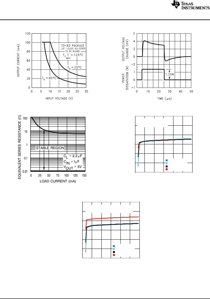
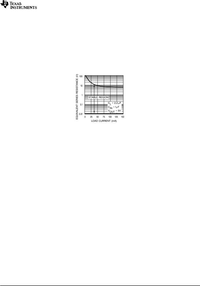
Output Capacitor Requirements
A 1.0 μF (or greater) capacitor is required between the output and ground for stability at output voltages of 5V or higher. At lower output voltages, more capacitance is required (2.2 μF or more is recommended for 3.0V and 3.3V versions). Without this capacitor the part will oscillate. Most types of tantalum or aluminum electrolytic work fine here; even film types work but are not recommended for reasons of cost. Many aluminum electrolytics have electrolytes that freeze at about −30°C, so solid tantalums are recommended for operation below −25°C. The important parameters of the capacitor are an ESR of about 5Ω or less and a resonant frequency above 500 kHz. The value of this capacitor may be increased without limit.
Figure 44. Output Capacitor ESR Range
The reason for the lower ESR limit is that the loop compensation of the feedback loop relies on the capacitance value and the ESR value of the output capacitor to provide the zero that gives added phase lead (See Figure 44).
fZ = (1 / (2 x π x COUT x ESR) ) |
(1) |
Using the 2.2 µF value from the Output Capacitor ESR Range curve (Figure 44), a useful range for fZ can be estimated:
fZ(MIN)= (1 / (2 x π x 2.2 µF x 5Ω) ) = 14.5 kHz |
(2) |
fZ(MAX)= (1 / (2 x π x 2.2 µF x 0.05Ω) ) = 318 kHz |
(3) |
For ceramic capacitors, the low ESR produces a zero at a frequency that is too high to be useful, so meaningful phase lead does not occur. A ceramic output capacitor can be used if a series resistance is added (recommended value of resistance about 0.1Ω to 2Ω) to simulate the needed ESR. Only X5R, X7R, or better, MLCC types should be used, and should have a DC voltage rating at least twice the VOUT(NOM) value.
At lower values of output current, less output capacitance is required for stability. The capacitor can be reduced to 0.33 μF for currents below 10 mA or 0.1 μF for currents below 1 mA. Using the adjustable versions at voltages below 5V runs the error amplifier at lower gains so that more output capacitance is needed. For the worst-case situation of a 100 mA load at 1.23V output (Output shorted to Feedback) a 3.3 μF (or greater) capacitor should be used.
Unlike many other regulators, the LP2950-N will remain stable and in regulation with no load in addition to the internal voltage divider. This is especially important in CMOS RAM keep-alive applications. When setting the output voltage of the LP2951-N versions with external resistors, a minimum load of 1 μA is recommended.
Applications having conditions that may drive the LP2950-N/51 into nonlinear operation require special consideration. Nonlinear operation will occur when the output voltage is held low enough to force the output stage into output current limiting while trying to pull the output voltage up to the regulated value. The internal loop response time will control how long it takes for the device to regain linear operation when the output has returned to the normal operating range. There are three significant nonlinear conditions that need to be considered, all can force the output stage into output current limiting mode, all can cause the output voltage to over-shoot with low
Copyright © 2000–2013, Texas Instruments Incorporated |
Submit Documentation Feedback |
13 |
Product Folder Links: LP2950-N LP2951-N
Loading...