


 Loading...
Texas Instruments LM3674MF, LM3674MF-1.2, LM3674MF-1.5, LM3674MF-1.8, LM3674MF-1.875 Schematic [ru]
...
|
|
|
|
|
LM3674 |
||
www.ti.com |
SNVS405F –DECEMBER 2005–REVISED MAY 2013 |
||||||
|
LM3674 2MHz, 600mA Step-Down DC-DC Converter in SOT-23 |
|
|
||||
|
Check for Samples: LM3674 |
|
|
|
|
||
|
|
|
|
|
|
||
FEATURES |
DESCRIPTION |
|
|
|
|
||
• 600mA Max Load Current |
The LM3674 step-down DC-DC converter is |
||||||
• Input Voltage Range from 2.7V to 5.5V |
optimized for powering low |
voltage |
circuits from |
a |
|||
single Li-Ion cell battery and input voltage rails from |
|||||||
• Available in Fixed and Adjustable Output |
|||||||
2.7V to 5.5V. It provides up to 600mA load current, |
|||||||
|
Voltages Ranging from 1.0V to 3.3V |
over the entire input voltage range. There are several |
|||||
• Operates from a Single Li-Ion Cell Battery |
fixed output voltages and adjustable output voltage |
||||||
• Internal Synchronous Rectification for High |
versions. |
|
|
|
|
||
The device offers superior features and performance |
|||||||
|
Efficiency |
||||||
• |
Internal Soft Start |
for mobile phones |
and similar portable systems. |
||||
During PWM mode, the device operates at a fixed- |
|||||||
• |
0.01 µ A Typical Shutdown Current |
||||||
frequency of 2 MHz (typ). Internal synchronous |
|||||||
• 2 MHz PWM Fixed Switching Frequency (typ) |
rectification provides high efficiency during Pulse |
||||||
• |
5-Pin SOT-23 Package |
Width Modulation |
(PWM) |
mode |
operation. |
In |
|
shutdown mode, the |
device |
turns off and reduces |
|||||
• Current Overload Protection and Thermal |
|||||||
battery consumption to 0.01 µA (typ). |
|
|
|||||
|
Shutdown Protection |
|
|
||||
|
The LM3674 is available in a 5-pin SOT-23 package |
||||||
|
|
||||||
APPLICATIONS |
in leaded (PB) and lead-free (NO PB) versions. A |
||||||
• |
Mobile Phones |
high switching frequency of 2 MHz (typ) allows use of |
|||||
only three tiny external surface-mount components, |
|||||||
• |
PDAs |
an inductor and two ceramic capacitors. |
|
||||
•MP3 Players
•Portable Instruments
•W-LAN
•Digital Still Cameras
•Portable Hard Disk Drives
TYPICAL APPLICATION CIRCUITS
VIN |
|
|
2.7V to 5.5V |
VIN |
|
|
1 |
5 |
CIN |
|
LM3674 |
4.7 PF |
|
|
GND |
|
|
|
|
|
|
2 |
|
|
EN |
4 |
|
3 |
|
|
|
L1:2.2 PH |
VOUT |
SW |
COUT
10 PF
FB
Figure 1. Typical Application Circuit
Please be aware that an important notice concerning availability, standard warranty, and use in critical applications of
Texas Instruments semiconductor products and disclaimers thereto appears at the end of this data sheet.
All trademarks are the property of their respective owners.
PRODUCTION DATA information is current as of publication date. |
Copyright © 2005–2013, Texas Instruments Incorporated |
Products conform to specifications per the terms of the Texas |
|
Instruments standard warranty. Production processing does not |
|
necessarily include testing of all parameters. |
|
LM3674
SNVS405F –DECEMBER 2005–REVISED MAY 2013 |
|
|
|
|
www.ti.com |
VIN |
VIN |
|
L1: 2.2 PH |
|
VOUT |
2.7V to 5.5V |
|
SW |
|
||
|
1 |
5 |
|
|
|
|
|
|
|
||
CIN: 4.7 PF |
LM3674- |
|
|
|
|
GND |
ADJ |
|
|
|
|
|
|
|
|
||
|
2 |
|
|
|
|
|
|
|
C1 |
R1 |
COUT: 10 PF |
|
EN |
|
FB |
|
|
34
C2 R2
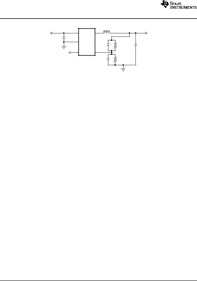
Figure 2. Typical Application Circuit for Adjustable Voltage Option
PIN DIAGRAM
SW |
FB |
54
|
|
|
|
|
|
|
|
|
|
|
|
|
|
|
|
|
|
|
|
|
|
VIN |
|
GND |
|
EN |
|
|
1 |
2 |
3 |
|
||
Figure 3. Top View
5-Pin SOT-23 Package
See Package Number DBV0005A
Note: The actual physical placement of the package marking will vary from part to part.
|
|
PIN DESCRIPTIONS |
|
Pin Number |
Name |
Description |
|
|
|
|
|
1 |
VIN |
Power supply input. Connect to the input filter capacitor ( Figure 1). |
|
2 |
GND |
Ground pin. |
|
|
|
|
|
3 |
EN |
Enable input. The device is in shutdown mode when voltage to this pin is <0.4V and enable when |
|
>1.0V. Do not leave this pin floating. |
|||
|
|
||
|
|
|
|
|
|
Feedback analog input. Connect to the output filter capacitor for fixed voltage versions. For adjustable |
|
4 |
FB |
version external resistor dividers are required ( Figure 2). The internal resistor dividers are disabled for |
|
|
|
the adjustable version. |
|
|
|
|
|
5 |
SW |
Switching node connection to the internal PFET switch and NFET synchronous rectifier. |
|
|
|
|
2 |
Submit Documentation Feedback |
Copyright © 2005–2013, Texas Instruments Incorporated |
Product Folder Links: LM3674

LM3674
www.ti.com |
SNVS405F –DECEMBER 2005–REVISED MAY 2013 |
These devices have limited built-in ESD protection. The leads should be shorted together or the device placed in conductive foam during storage or handling to prevent electrostatic damage to the MOS gates.
|
ORDERING INFORMATION(1) (2) |
|
LM3674 (5 Pin SOT-23) |
|
|
|
|
|
Ordering Information |
|
Voltage Option (V) |
|
|
|
LM3674MF-1.2 |
|
|
|
|
|
LM3674MFX-1.2 |
|
1.2 |
|
|
|
LM3674MF-1.2/NOPB |
|
|
|
|
|
|
|
|
LM3674MFX-1.2/NOPB |
|
|
|
|
|
LM3674MF-1.5 |
|
|
|
|
|
LM3674MFX-1.5 |
|
1.5 |
|
|
|
LM3674MF-1.5/NOPB |
|
|
|
|
|
|
|
|
LM3674MFX-1.5/NOPB |
|
|
|
|
|
LM3674MF-1.6 |
|
|
|
|
|
LM3674MFX-1.6 |
|
1.6 |
|
|
|
LM3674MF-1.6/NOPB |
|
|
|
|
|
|
|
|
LM3674MFX-1.6/NOPB |
|
|
|
|
|
LM3674MF-1.8 |
|
|
|
|
|
LM3674MFX-1.8 |
|
1.8 |
|
|
|
LM3674MF-1.8/NOPB |
|
|
|
|
|
|
|
|
LM3674MFX-1.8/NOPB |
|
|
|
|
|
LM3674MF-1.875 |
|
|
|
|
|
LM3674MFX-1.875 |
|
1.875 |
|
|
|
LM3674MF-1.875/NOPB |
|
|
|
|
|
|
|
|
LM3674MFX-1.875/NOPB |
|
|
|
|
|
LM3674MF-2.8 |
|
|
|
|
|
LM3674MFX-2.8 |
|
2.8 |
|
|
|
LM3674MF-2.8/NOPB |
|
|
|
|
|
|
|
|
LM3674MFX-2.8/NOPB |
|
|
|
|
|
LM3674MF-ADJ |
|
|
|
|
|
LM3674MFX-ADJ |
|
Adjustable |
|
|
|
LM3674MF-ADJ/NOPB |
|
|
|
|
|
|
|
|
LM3674MFX-ADJ/NOPB |
|
|
|
|
|
(1)For the most current package and ordering information, see the Package Option Addendum at the end of this document, or see the TI web site at www.ti.com.
(2)Package drawings, thermal data, and symbolization are available at www.ti.com/packaging.
Copyright © 2005–2013, Texas Instruments Incorporated |
Submit Documentation Feedback |
3 |
Product Folder Links: LM3674

LM3674
SNVS405F –DECEMBER 2005–REVISED MAY 2013 www.ti.com
Absolute Maximum Ratings(1) (2)
VIN Pin: Voltage to GND |
−0.2V to 6.0V |
EN, FB, SW Pin: |
(GND−0.2V) to |
|
(VIN + 0.2V) |
Continuous Power Dissipation(3) |
Internally Limited |
Junction Temperature (TJ-MAX) |
+125°C |
Storage Temperature Range |
−65°C to +150°C |
Maximum Lead Temperature |
260°C |
(Soldering, 10 sec.) |
|
|
|
ESD Rating(4) |
2 kV |
Human Body model: All Pins |
|
|
|
Machine Model: All Pins |
200V |
|
|
(1)Absolute Maximum Ratings indicate limits beyond which damage to the device may occur. Operating Ratings are conditions under which operation of the device is ensured. Operating Ratings may not imply performance limits. For performance limits and associated test conditions, see the Electrical Characteristics tables.
(2)If Military/Aerospace specified devices are required, please contact the TI Sales Office/Distributors for availability and specifications.
(3)In Applications where high power dissipation and /or poor package resistance is present, the maximum ambient temperature may have
to be derated. Maximum ambient temperature (TA-MAX ) is dependent on the maximum operating junction temperature (TJ-MAX ), the maximum power dissipation of the device in the application (PD-MAX ) and the junction to ambient thermal resistance of the package (θJA) in the application, as given by the following equation: TA-MAX = TJ-MAX- (θJA x PD-MAX). Refer to Dissipation ration table for PD-MAX values at different ambient temperatures.
(4)The Human body model is a 100 pF capacitor discharged through a 1.5 kΩ resistor into each pin. The machine model is a 200 pF capacitor discharged directly into each pin (MIL-STD-883 3015.7). National Semiconductor recommends that all intergrated circuits be handled with appropriate precautions. Failure to observe proper ESD handling techniques can result in damage.
Operating Ratings(1) (2) (3)
Input Voltage Range(4) |
2.7V to 5.5V |
Recommended Load Current |
0A to 600 mA |
|
|
Junction Temperature (TJ) Range |
−30°C to +125°C |
Ambient Temperature (TA) Range |
−30°C to +85°C |
(1)In Applications where high power dissipation and /or poor package resistance is present, the maximum ambient temperature may have
to be derated. Maximum ambient temperature (TA-MAX ) is dependent on the maximum operating junction temperature (TJ-MAX ), the maximum power dissipation of the device in the application (PD-MAX ) and the junction to ambient thermal resistance of the package (θJA) in the application, as given by the following equation: TA-MAX = TJ-MAX- (θJA x PD-MAX). Refer to Dissipation ration table for PD-MAX values at different ambient temperatures.
(2)Absolute Maximum Ratings indicate limits beyond which damage to the device may occur. Operating Ratings are conditions under which operation of the device is ensured. Operating Ratings may not imply performance limits. For performance limits and associated test conditions, see the Electrical Characteristics tables.
(3)All voltages are with respect to the potential at the GND pin.
(4)Input voltage range recommended for ideal applications performance for the specified output voltages are given below
VIN = 2.7V to 5.5V for 1.0V ≤ VOUT < 1.8V
VIN = ( VOUT + VDROP OUT) to 5.5V for 1.8 ≤ VOUT≤ 3.3V Where VDROP OUT = ILOAD * (RDSON (P) + RINDUCTOR)
Thermal Properties(1)
over operating free-air temperature range (unless otherwise noted)
Junction-to-Ambient Thermal Resistance (θJA) (SOT-23) for a 2 layer board (2) |
250°C/W |
Junction-to-Ambient Thermal Resistance (θJA) (SOT-23) for a 4 layer board (2) |
130°C/W |
(1)Internal thermal shutdown circuitry protects the device from permanent damage. Thermal shutdown engages at TJ = 150°C (typ.) and disengages at TJ = 130°C
(2)Junction to ambient thermal resistance (θJA) is highly application and board layout dependent. In applications where high power dissipation exists, special care must be given to thermal dissipation issues in board design. Value specified here 250°C/W is based on
measurement results using a 2 layer, 4" X 3", 2 oz. Cu board as per JEDEC standards. The θJA is 130°C/W if a 4 layer, 4" X 3", 2/1/1/2 oz. Cu board as per JEDEC standards is used.
4 |
Submit Documentation Feedback |
Copyright © 2005–2013, Texas Instruments Incorporated |
Product Folder Links: LM3674

LM3674
www.ti.com |
SNVS405F –DECEMBER 2005–REVISED MAY 2013 |
Electrical Characteristics(1) (2) (3)
Limits in standard typeface are for TJ = 25°C. Limits in boldface type apply over the full operating junction temperature range (−30°C ≤ TJ ≤ 125°C). Unless otherwise noted, specifications apply to the LM3674 with VIN = EN = 3.6V
|
Parameter |
Test Condition |
Min |
Typ |
Max |
Units |
|
|
|
|
|
|
|
V |
Feedback Voltage(4)(5) |
I = 10mA |
-4 |
|
+4 |
% |
FB |
|
O |
|
|
|
|
|
Line Regulation |
2.7V ≤ VIN ≤ 5.5V |
|
0.083 |
|
%/V |
|
|
IO = 100 mA |
|
|
|
|
|
Load Regulation |
100 mA ≤ IO ≤ 600 mA |
|
0.0010 |
|
%/mA |
|
|
VIN = 3.6V |
|
|
|
|
V |
Internal Reference Voltage |
See (6) |
|
0.5 |
|
V |
REF |
|
|
|
|
|
|
ISHDN |
Shutdown Supply Current |
EN = 0V |
|
0.01 |
1 |
µA |
IQ |
DC Bias Current into VIN |
No load, device is not switching |
|
300 |
600 |
µA |
|
|
(FB=0V) |
|
|
|
|
RDSON (P) |
Pin-Pin Resistance for PFET |
ISW = 200mA |
|
380 |
500 |
mΩ |
RDSON (N) |
Pin-Pin Resistance for NFET |
ISW = 200mA |
|
250 |
400 |
mΩ |
I |
Switch Peak Current Limit |
Open Loop (7) |
830 |
1020 |
1200 |
mA |
LIM |
|
|
|
|
|
|
VIH |
Logic High Input |
|
1.0 |
|
|
V |
VIL |
Logic Low Input |
|
|
|
0.4 |
V |
IEN |
Enable (EN) Input Current |
|
|
0.01 |
1 |
µA |
FOSC |
Internal Oscillator Frequency |
PWM Mode |
1.6 |
2 |
2.6 |
MHz |
(1)All voltages are with respect to the potential at the GND pin.
(2)Min and Max limits are specified by design, test or statistical analysis. Typical numbers represent the most likely norm.
(3)The parameters in the electrical characteristic table are tested at VIN = 3.6V unless otherwise specified. For performance over the input voltage range refer to datasheet curves.
(4)ADJ configured to 1.5V output.
(5)For VOUT less than 2.5V, VIN = 3.6V, for VOUT greater than or equal to 2.5V, VIN = VOUT +1.
(6)For the ADJ version the resistor dividers should be selected such that at the desired output voltage, the voltage at the FB pin is 0.5V.
(7)Refer to datasheet curves for closed loop data and its variation with regards to supply voltage and temperature. Electrical Characteristic table reflects open loop data (FB=0V and current drawn from SW pin ramped up until cycle by cycle current limit is activated). Closed loop current limit is the peak inductor current measured in the application circuit by increasing output current until output voltage drops by 10%.
Dissipation Rating
over operating free-air temperature range (unless otherwise noted)
θJA |
TA ≤ 25°C (Power Rating) |
TA = 60°C (Power Rating) |
TA = 85°C (Power Rating) |
250°C/W (2 layer board) |
400mW |
260mW |
160mW |
|
|
|
|
130°C/W (4 layer board) |
770mW |
500mW |
310mW |
|
|
|
|
Copyright © 2005–2013, Texas Instruments Incorporated |
Submit Documentation Feedback |
5 |
Product Folder Links: LM3674
LM3674
SNVS405F –DECEMBER 2005–REVISED MAY 2013
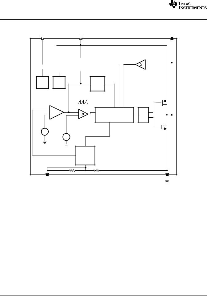
Block Diagram
|
EN |
|
VIN |
|
|
|
|
|
|
|
|
|
|
|
|
|
Undervoltage |
|
Ramp |
|
Soft |
|
|
|
Lockout |
|
Generator |
|
Start |
|
|
|
|
|
|
|
|
|
|
|
|
|
|
|
|
|
|
|
|
|
|
|
|
|
|
Thermal |
Bandgap |
2 MHz |
|
Shutdown |
|||
|
Oscillator |
||
|
|
|
|
|
PWM Comparator |
|
|
Error |
|
+ |
|
|
Amp |
|
|
|
|
|
- |
Control Logic |
|
|
|
|
||
|
|
|
|
|
VREF |
|
|
|
|
0.5V + |
|
|
|
|
- |
|
+ Vcomp |
|
|
|
|
|
||
|
|
- |
1.0V |
|
|
|
|
|
|
Frequency |
Compensation |
Adjustable Version
Fixed Version
FB
www.ti.com
SW
Current Limit
Comparator
+ |
|
|
|
Ref1 |
|
- |
|
|
|
Driver
GND
Figure 4. Simplified Functional Block Diagram
6 |
Submit Documentation Feedback |
Copyright © 2005–2013, Texas Instruments Incorporated |
Product Folder Links: LM3674

LM3674
www.ti.com |
SNVS405F –DECEMBER 2005–REVISED MAY 2013 |
Typical Performance Characteristics
(unless otherwise stated: VIN = 3.6V, VOUT = 1.5V, TA = 25°C)
Quiescent Current vs. Supply Voltage (FB = 0V, No Switching)
IQ Shutdown vs. Temp
0.40
EN = GND
A)(P |
0.35 |
|
|
|
|
|
|
0.30 |
|
|
|
|
|
|
|
CURRENT |
|
|
|
|
|
|
|
0.25 |
|
|
|
|
|
|
|
0.20 |
|
|
|
VIN = 5.5V |
|
|
|
SHUTDOWN |
|
|
|
|
|
|
|
0.15 |
|
|
VIN = 3.6V |
|
|
||
|
|
|
|
|
|||
0.10 |
|
|
VIN = 2.7V |
|
|
||
0.05 |
|
|
|
|
|||
|
|
|
|
|
|
|
|
|
0.00 |
|
|
|
|
|
|
|
-30 |
-10 |
10 |
30 |
50 |
70 |
90 |
|
|
|
TEMPERATURE (°C) |
|
|
||
Figure 5. |
Figure 6. |
Feedback Bias Current vs. Temp |
Output Voltage vs. Supply Voltage |
Figure 7. |
Figure 8. |
Output Voltage vs. Temperature |
Output Voltage vs. Output Current |
Figure 9. |
Figure 10. |
Copyright © 2005–2013, Texas Instruments Incorporated |
Submit Documentation Feedback |
7 |
Product Folder Links: LM3674

LM3674
SNVS405F –DECEMBER 2005–REVISED MAY 2013 |
www.ti.com |
Typical Performance Characteristics (continued)
(unless otherwise stated: VIN = 3.6V, VOUT = 1.5V, TA = 25°C)
RDSON vs. Temperature
|
600 |
VIN = 2.7V |
|
|
550 |
||
|
VIN = 4.5V |
||
|
500 |
||
|
VIN = 3.6V |
||
): |
450 |
|
|
400 |
PFET |
||
|
|||
m |
VIN = 2.7V |
||
( |
|
||
(ON)DS |
350 |
||
|
|||
300 |
|
||
R |
|
VIN = 4.5V |
|
|
250 |
||
|
200 |
NFET |
|
|
|
||
|
150 |
VIN = 3.6V |
|
|
100 |
|
|
|
-30 |
-10 10 30 50 70 90 110 |
|
|
|
TEMPERATURE (°C) |
Figure 11.
Efficiency vs. Output Current (VOUT = 1.5V, L = 2.2uH, DCR = 200mΩ)
Efficiency vs. Output Current (VOUT = 1.2V, L = 2.2uH, DCR = 200mΩ)
Figure 12.
Efficiency vs. Output Current (VOUT = 1.8V, L = 2.2uH, DCR = 200mΩ)
Figure 13. |
Figure 14. |
Efficiency vs. Output Current (VOUT = 3.3V, L = 2.2uH, DCR = 200mΩ)
Switching Frequency vs. Temperature
|
2.00 |
|
|
|
IOUT = 300 mA |
|
|
|
|
|
|
|
|
||
|
1.98 |
VIN = 4.5V |
|
|
|
|
|
|
_ |
|
|
|
|
|
|
|
1.96 |
|
|
VIN = 3.6V |
|
|
|
(MHZ) |
|
|
|
|
|
|
|
_ |
|
|
|
|
|
|
|
|
|
|
VIN = 2.7V |
|
|
||
FREQUENCY |
1.94 |
|
|
|
|
||
|
|
|
|
|
|
||
_ |
|
|
|
|
|
|
|
1.92 |
|
|
|
|
|
|
|
_ |
|
|
|
|
|
|
|
|
|
|
|
|
|
|
|
|
1.90 |
|
|
|
|
|
|
|
_ |
|
|
|
|
|
|
|
1.88 |
- |
|
|
|
|
|
|
_-30 |
10 |
|
50 |
70 |
90 |
|
|
10 |
30 |
|||||
|
|
_ |
_ |
|
_ |
_ |
_ |
|
|
TEMPERATURE (°C) |
|
|
|||
|
Figure 15. |
Figure 16. |
|
|
|
8 |
Submit Documentation Feedback |
Copyright © 2005–2013, Texas Instruments Incorporated |
Product Folder Links: LM3674
Loading...